KR20090056077A - 인쇄회로기판과 그 제조방법 및 인쇄회로기판 제조용 패널 - Google Patents
인쇄회로기판과 그 제조방법 및 인쇄회로기판 제조용 패널 Download PDFInfo
- Publication number
- KR20090056077A KR20090056077A KR1020070123059A KR20070123059A KR20090056077A KR 20090056077 A KR20090056077 A KR 20090056077A KR 1020070123059 A KR1020070123059 A KR 1020070123059A KR 20070123059 A KR20070123059 A KR 20070123059A KR 20090056077 A KR20090056077 A KR 20090056077A
- Authority
- KR
- South Korea
- Prior art keywords
- printed circuit
- circuit board
- region
- insulating member
- manufacturing
- Prior art date
- Legal status (The legal status is an assumption and is not a legal conclusion. Google has not performed a legal analysis and makes no representation as to the accuracy of the status listed.)
- Ceased
Links
- 238000004519 manufacturing process Methods 0.000 title claims abstract description 40
- 238000000034 method Methods 0.000 claims abstract description 20
- 239000004020 conductor Substances 0.000 claims abstract description 10
- 239000011241 protective layer Substances 0.000 claims description 8
- 239000007769 metal material Substances 0.000 claims description 6
- 229920002120 photoresistant polymer Polymers 0.000 description 14
- 239000000463 material Substances 0.000 description 7
- 238000009713 electroplating Methods 0.000 description 6
- RYGMFSIKBFXOCR-UHFFFAOYSA-N Copper Chemical compound [Cu] RYGMFSIKBFXOCR-UHFFFAOYSA-N 0.000 description 4
- 229910052802 copper Inorganic materials 0.000 description 4
- 239000010949 copper Substances 0.000 description 4
- 239000010408 film Substances 0.000 description 4
- 238000007747 plating Methods 0.000 description 4
- 229910000679 solder Inorganic materials 0.000 description 2
- 239000004593 Epoxy Substances 0.000 description 1
- 240000001417 Vigna umbellata Species 0.000 description 1
- 235000011453 Vigna umbellata Nutrition 0.000 description 1
- 239000011248 coating agent Substances 0.000 description 1
- 238000000576 coating method Methods 0.000 description 1
- 150000001875 compounds Chemical class 0.000 description 1
- 230000000694 effects Effects 0.000 description 1
- 238000005516 engineering process Methods 0.000 description 1
- 238000005530 etching Methods 0.000 description 1
- 239000012530 fluid Substances 0.000 description 1
- 239000003365 glass fiber Substances 0.000 description 1
- 230000010354 integration Effects 0.000 description 1
- 239000007788 liquid Substances 0.000 description 1
- 239000002184 metal Substances 0.000 description 1
- 229910052751 metal Inorganic materials 0.000 description 1
- 238000012986 modification Methods 0.000 description 1
- 230000004048 modification Effects 0.000 description 1
- 239000005011 phenolic resin Substances 0.000 description 1
- 238000005728 strengthening Methods 0.000 description 1
- 239000000126 substance Substances 0.000 description 1
- 239000010409 thin film Substances 0.000 description 1
Images


Classifications
-
- H—ELECTRICITY
- H05—ELECTRIC TECHNIQUES NOT OTHERWISE PROVIDED FOR
- H05K—PRINTED CIRCUITS; CASINGS OR CONSTRUCTIONAL DETAILS OF ELECTRIC APPARATUS; MANUFACTURE OF ASSEMBLAGES OF ELECTRICAL COMPONENTS
- H05K3/00—Apparatus or processes for manufacturing printed circuits
- H05K3/0097—Processing two or more printed circuits simultaneously, e.g. made from a common substrate, or temporarily stacked circuit boards
-
- H—ELECTRICITY
- H05—ELECTRIC TECHNIQUES NOT OTHERWISE PROVIDED FOR
- H05K—PRINTED CIRCUITS; CASINGS OR CONSTRUCTIONAL DETAILS OF ELECTRIC APPARATUS; MANUFACTURE OF ASSEMBLAGES OF ELECTRICAL COMPONENTS
- H05K1/00—Printed circuits
- H05K1/02—Details
-
- H—ELECTRICITY
- H05—ELECTRIC TECHNIQUES NOT OTHERWISE PROVIDED FOR
- H05K—PRINTED CIRCUITS; CASINGS OR CONSTRUCTIONAL DETAILS OF ELECTRIC APPARATUS; MANUFACTURE OF ASSEMBLAGES OF ELECTRICAL COMPONENTS
- H05K1/00—Printed circuits
- H05K1/02—Details
- H05K1/0271—Arrangements for reducing stress or warp in rigid printed circuit boards, e.g. caused by loads, vibrations or differences in thermal expansion
-
- H—ELECTRICITY
- H05—ELECTRIC TECHNIQUES NOT OTHERWISE PROVIDED FOR
- H05K—PRINTED CIRCUITS; CASINGS OR CONSTRUCTIONAL DETAILS OF ELECTRIC APPARATUS; MANUFACTURE OF ASSEMBLAGES OF ELECTRICAL COMPONENTS
- H05K2201/00—Indexing scheme relating to printed circuits covered by H05K1/00
- H05K2201/09—Shape and layout
- H05K2201/09209—Shape and layout details of conductors
- H05K2201/0929—Conductive planes
- H05K2201/09354—Ground conductor along edge of main surface
-
- H—ELECTRICITY
- H05—ELECTRIC TECHNIQUES NOT OTHERWISE PROVIDED FOR
- H05K—PRINTED CIRCUITS; CASINGS OR CONSTRUCTIONAL DETAILS OF ELECTRIC APPARATUS; MANUFACTURE OF ASSEMBLAGES OF ELECTRICAL COMPONENTS
- H05K2201/00—Indexing scheme relating to printed circuits covered by H05K1/00
- H05K2201/09—Shape and layout
- H05K2201/09209—Shape and layout details of conductors
- H05K2201/09654—Shape and layout details of conductors covering at least two types of conductors provided for in H05K2201/09218 - H05K2201/095
- H05K2201/09736—Varying thickness of a single conductor; Conductors in the same plane having different thicknesses
-
- H—ELECTRICITY
- H05—ELECTRIC TECHNIQUES NOT OTHERWISE PROVIDED FOR
- H05K—PRINTED CIRCUITS; CASINGS OR CONSTRUCTIONAL DETAILS OF ELECTRIC APPARATUS; MANUFACTURE OF ASSEMBLAGES OF ELECTRICAL COMPONENTS
- H05K2201/00—Indexing scheme relating to printed circuits covered by H05K1/00
- H05K2201/09—Shape and layout
- H05K2201/09209—Shape and layout details of conductors
- H05K2201/09654—Shape and layout details of conductors covering at least two types of conductors provided for in H05K2201/09218 - H05K2201/095
- H05K2201/09781—Dummy conductors, i.e. not used for normal transport of current; Dummy electrodes of components
-
- H—ELECTRICITY
- H05—ELECTRIC TECHNIQUES NOT OTHERWISE PROVIDED FOR
- H05K—PRINTED CIRCUITS; CASINGS OR CONSTRUCTIONAL DETAILS OF ELECTRIC APPARATUS; MANUFACTURE OF ASSEMBLAGES OF ELECTRICAL COMPONENTS
- H05K2201/00—Indexing scheme relating to printed circuits covered by H05K1/00
- H05K2201/20—Details of printed circuits not provided for in H05K2201/01 - H05K2201/10
- H05K2201/2009—Reinforced areas, e.g. for a specific part of a flexible printed circuit
-
- H—ELECTRICITY
- H05—ELECTRIC TECHNIQUES NOT OTHERWISE PROVIDED FOR
- H05K—PRINTED CIRCUITS; CASINGS OR CONSTRUCTIONAL DETAILS OF ELECTRIC APPARATUS; MANUFACTURE OF ASSEMBLAGES OF ELECTRICAL COMPONENTS
- H05K2203/00—Indexing scheme relating to apparatus or processes for manufacturing printed circuits covered by H05K3/00
- H05K2203/01—Tools for processing; Objects used during processing
- H05K2203/0147—Carriers and holders
- H05K2203/0169—Using a temporary frame during processing
-
- H—ELECTRICITY
- H05—ELECTRIC TECHNIQUES NOT OTHERWISE PROVIDED FOR
- H05K—PRINTED CIRCUITS; CASINGS OR CONSTRUCTIONAL DETAILS OF ELECTRIC APPARATUS; MANUFACTURE OF ASSEMBLAGES OF ELECTRICAL COMPONENTS
- H05K3/00—Apparatus or processes for manufacturing printed circuits
- H05K3/0011—Working of insulating substrates or insulating layers
- H05K3/0044—Mechanical working of the substrate, e.g. drilling or punching
- H05K3/0052—Depaneling, i.e. dividing a panel into circuit boards; Working of the edges of circuit boards
Landscapes
- Engineering & Computer Science (AREA)
- Microelectronics & Electronic Packaging (AREA)
- Manufacturing & Machinery (AREA)
- Structure Of Printed Boards (AREA)
- Manufacturing Of Printed Wiring (AREA)
Abstract
Description
Claims (12)
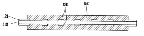
- 적어도 어느 일면에 형성되는 제1영역과, 상기 제1영역의 가장자리에 형성되는 제2영역을 구비하는 절연부재;상기 제1영역에 구비되는 도전성 재질의 회로 패턴; 및상기 제2영역에 구비되어 상기 절연부재가 평면 형태를 유지하도록 상기 절연부재를 지지하는 지지부재를 포함하는 인쇄회로기판.
- 제1항에 있어서,상기 절연부재의 두께는 130㎛이하로 형성되는 것을 특징으로 하는 인쇄회로기판.
- 제1항에 있어서,상기 지지부재는 금속 재질로 형성되며, 일정 폭을 갖는 밴드 형태로 형성되는 것을 특징으로 하는 인쇄회로기판.
- 제1항에 있어서,상기 제2영역에는 도전성 재질의 도전패턴이 더 구비되고,상기 지지부재는 상기 도전패턴의 상면에 형성되는 것을 특징으로 하는 인쇄회로기판.
- 제1항에 있어서,상기 절연부재, 회로패턴, 및 지지부재의 표면을 덮도록 구비되어 이들을 외부로부터 보호하는 보호층을 더 포함하는 것을 특징으로 하는 인쇄회로기판.
- 복수의 개소에 형성되는 제1영역들과, 상기 제1영역들을 제외한 나머지 영역에 형성되는 제2영역을 구비하는 프레임;상기 제1영역들에 각각 구비되는 복수의 인쇄회로기판들; 및상기 제2영역에 구비되어 상기 프레임이 평면 형태를 유지하도록 상기 프레임을 지지하는 지지부재를 포함하는 인쇄회로기판 제조용 패널.
- 제6항에 있어서,상기 인쇄회로기판의 두께는 130㎛이하로 형성되고, 상기 지지부재는 금속재질로 형성되는 것을 특징으로 하는 인쇄회로기판 제조용 패널.
- 절연부재의 제1영역에 도전성 재질의 회로패턴이 형성되는 단계; 및상기 제1영역의 가장자리에 형성된 제2영역에 상기 절연부재가 평면 형태를 유지하도록 상기 절연부재를 지지하는 지지부재가 형성되는 단계를 포함하는 인쇄회로기판의 제조방법.
- 제8항에 있어서, 상기 지지부재가 형성되는 단계는,상기 절연부재의 일면에 기초부재가 형성되는 단계;상기 기초부재 중 상기 제2영역에 상응하는 부분이 제거되는 단계;상기 제2영역에 상기 지지부재가 형성되는 단계; 및상기 기초부재가 제거되는 단계를 포함하는 것을 특징으로 하는 인쇄회로기판의 제조방법.
- 제8항에 있어서,상기 절연부재의 두께는 130㎛이하로 형성되는 것을 특징으로 하는 인쇄회로기판의 제조방법.
- 제8항에 있어서,상기 지지부재는 금속 재질로 형성되며, 일정 폭을 갖는 밴드 형태로 형성되는 것을 특징으로 하는 인쇄회로기판의 제조방법.
- 제8항에 있어서,상기 절연부재, 회로패턴, 및 지지부재의 표면에 이들을 외부로부터 보호하는 보호층이 형성되는 단계를 더 포함하는 것을 특징으로 하는 인쇄회로기판의 제조방법.
Priority Applications (6)
| Application Number | Priority Date | Filing Date | Title |
|---|---|---|---|
| KR1020070123059A KR20090056077A (ko) | 2007-11-29 | 2007-11-29 | 인쇄회로기판과 그 제조방법 및 인쇄회로기판 제조용 패널 |
| TW097146120A TWI440407B (zh) | 2007-11-29 | 2008-11-28 | 印刷電路板及其製造方法和製造印刷電路板之製作面板 |
| US12/745,667 US8426739B2 (en) | 2007-11-29 | 2008-12-01 | Printed circuit board and method for manufacturing the same, and panel for manufacturing the printed circuit board |
| PCT/KR2008/007088 WO2009069987A2 (en) | 2007-11-29 | 2008-12-01 | Printed circuit board and method for manufacturing the same, and panel for manufacturing the printed circuit board |
| CN2008801236813A CN101919319A (zh) | 2007-11-29 | 2008-12-01 | 印刷电路板及其制造方法及用于制造该印刷电路板的面板 |
| JP2010535890A JP5426567B2 (ja) | 2007-11-29 | 2008-12-01 | プリント回路基板及びその製造方法並びにプリント回路基板製造用のパネル |
Applications Claiming Priority (1)
| Application Number | Priority Date | Filing Date | Title |
|---|---|---|---|
| KR1020070123059A KR20090056077A (ko) | 2007-11-29 | 2007-11-29 | 인쇄회로기판과 그 제조방법 및 인쇄회로기판 제조용 패널 |
Publications (1)
| Publication Number | Publication Date |
|---|---|
| KR20090056077A true KR20090056077A (ko) | 2009-06-03 |
Family
ID=40679164
Family Applications (1)
| Application Number | Title | Priority Date | Filing Date |
|---|---|---|---|
| KR1020070123059A Ceased KR20090056077A (ko) | 2007-11-29 | 2007-11-29 | 인쇄회로기판과 그 제조방법 및 인쇄회로기판 제조용 패널 |
Country Status (6)
| Country | Link |
|---|---|
| US (1) | US8426739B2 (ko) |
| JP (1) | JP5426567B2 (ko) |
| KR (1) | KR20090056077A (ko) |
| CN (1) | CN101919319A (ko) |
| TW (1) | TWI440407B (ko) |
| WO (1) | WO2009069987A2 (ko) |
Cited By (1)
| Publication number | Priority date | Publication date | Assignee | Title |
|---|---|---|---|---|
| KR20230143028A (ko) * | 2022-04-04 | 2023-10-11 | 주식회사 심텍 | 더미 프레임을 이용하는 인쇄회로기판의 제조 방법 |
Families Citing this family (5)
| Publication number | Priority date | Publication date | Assignee | Title |
|---|---|---|---|---|
| TWI560454B (en) * | 2014-11-07 | 2016-12-01 | Primax Electronics Ltd | Testing base |
| EP3339021B1 (en) * | 2015-09-30 | 2020-05-06 | Sekisui Chemical Co., Ltd. | Laminated body |
| JP7065617B2 (ja) * | 2018-01-12 | 2022-05-12 | 新光電気工業株式会社 | 支持体付基板及びその製造方法 |
| CN109275272A (zh) * | 2018-11-27 | 2019-01-25 | 景旺电子科技(龙川)有限公司 | 一种薄pcb板处理方法 |
| KR20210154450A (ko) * | 2020-06-12 | 2021-12-21 | 엘지이노텍 주식회사 | 인쇄회로기판 및 이의 제조 방법 |
Family Cites Families (13)
| Publication number | Priority date | Publication date | Assignee | Title |
|---|---|---|---|---|
| JPS5667982A (en) | 1979-11-07 | 1981-06-08 | Tdk Electronics Co Ltd | Printed circuit board and method of manufacturing same |
| JPS62124571U (ko) * | 1986-01-31 | 1987-08-07 | ||
| JPH0680872B2 (ja) | 1988-11-29 | 1994-10-12 | 日本電気株式会社 | フレキシブルプリント基板シート |
| JP3437369B2 (ja) * | 1996-03-19 | 2003-08-18 | 松下電器産業株式会社 | チップキャリアおよびこれを用いた半導体装置 |
| US6020221A (en) * | 1996-12-12 | 2000-02-01 | Lsi Logic Corporation | Process for manufacturing a semiconductor device having a stiffener member |
| JPH11214806A (ja) * | 1998-01-23 | 1999-08-06 | Nec Saitama Ltd | プリント基板補強構造 |
| JP2000164997A (ja) * | 1998-11-27 | 2000-06-16 | Denso Corp | プリント基板およびプリント基板への部品実装方法 |
| JP3635219B2 (ja) * | 1999-03-11 | 2005-04-06 | 新光電気工業株式会社 | 半導体装置用多層基板及びその製造方法 |
| US6204559B1 (en) * | 1999-11-22 | 2001-03-20 | Advanced Semiconductor Engineering, Inc. | Ball grid assembly type semiconductor package having improved chip edge support to prevent chip cracking |
| JP2003209366A (ja) * | 2002-01-15 | 2003-07-25 | Sony Corp | フレキシブル多層配線基板およびその製造方法 |
| EP1520454B1 (en) * | 2002-06-27 | 2012-01-25 | PPG Industries Ohio, Inc. | Single or multi-layer printed circuit board with extended breakaway tabs and method of manufacture thereof |
| KR100992637B1 (ko) * | 2003-07-24 | 2010-11-05 | 엘지이노텍 주식회사 | 인쇄회로기판 제조용 모재와 그를 사용한 인쇄회로기판의제조방법 |
| KR100736633B1 (ko) * | 2005-12-19 | 2007-07-06 | 삼성전기주식회사 | 보강 기판 및 제조 방법 |
-
2007
- 2007-11-29 KR KR1020070123059A patent/KR20090056077A/ko not_active Ceased
-
2008
- 2008-11-28 TW TW097146120A patent/TWI440407B/zh active
- 2008-12-01 WO PCT/KR2008/007088 patent/WO2009069987A2/en not_active Ceased
- 2008-12-01 JP JP2010535890A patent/JP5426567B2/ja active Active
- 2008-12-01 US US12/745,667 patent/US8426739B2/en active Active
- 2008-12-01 CN CN2008801236813A patent/CN101919319A/zh active Pending
Cited By (1)
| Publication number | Priority date | Publication date | Assignee | Title |
|---|---|---|---|---|
| KR20230143028A (ko) * | 2022-04-04 | 2023-10-11 | 주식회사 심텍 | 더미 프레임을 이용하는 인쇄회로기판의 제조 방법 |
Also Published As
| Publication number | Publication date |
|---|---|
| WO2009069987A2 (en) | 2009-06-04 |
| US8426739B2 (en) | 2013-04-23 |
| JP2011505690A (ja) | 2011-02-24 |
| JP5426567B2 (ja) | 2014-02-26 |
| WO2009069987A3 (en) | 2009-08-20 |
| TWI440407B (zh) | 2014-06-01 |
| CN101919319A (zh) | 2010-12-15 |
| US20110036618A1 (en) | 2011-02-17 |
| TW200934310A (en) | 2009-08-01 |
Similar Documents
| Publication | Publication Date | Title |
|---|---|---|
| CN1319423C (zh) | 印刷线路板及半导体装置 | |
| US7799603B2 (en) | Method for mounting electronic component on printed circuit board | |
| KR20090056077A (ko) | 인쇄회로기판과 그 제조방법 및 인쇄회로기판 제조용 패널 | |
| EP1971194A2 (en) | Wiring substrate and manufacturing method thereof | |
| KR101847163B1 (ko) | 인쇄회로기판 및 그 제조방법 | |
| US8067696B2 (en) | Printed circuit board and method for manufacturing same | |
| KR20050061343A (ko) | 배선 회로 기판 | |
| US20130240254A1 (en) | Printed circuit board and method for manufacturing printed circuit board | |
| CN113811074A (zh) | 印制电路板制作方法、金手指保护方法和保护结构 | |
| KR20140019689A (ko) | 인쇄회로기판 및 그 제조방법 | |
| CN216217750U (zh) | 一种电镀式阶梯焊盘pcb | |
| KR101317952B1 (ko) | 트랜스퍼 몰드 방식을 이용한 led모듈의 칩온보드 댐 제조방법 및 그 제조방법에 의한 led 모듈 | |
| KR101004583B1 (ko) | 회로기판 모듈용 지그 | |
| JP3985140B2 (ja) | 配線基板の製造方法 | |
| KR101022869B1 (ko) | 이미지센서 모듈용 인쇄회로기판의 제조방법 | |
| US20090266587A1 (en) | Flexible printed circuit board and method of forming fine pitch therein | |
| KR100425728B1 (ko) | 인쇄회로기판의 홀 충진방법 및 그 장치 및인쇄회로기판의 제조방법 | |
| KR20150107141A (ko) | 인쇄회로기판 및 그의 제조 방법 | |
| KR100818328B1 (ko) | 필름 캐리어 테이프의 제조 방법 | |
| KR102096083B1 (ko) | 보강판 패널 및 이의 제조 방법 | |
| KR20070062079A (ko) | 위치 정렬 마크를 갖는 인쇄회로기판과 그 제조 방법 | |
| KR100660154B1 (ko) | 필름 캐리어 테이프의 제조 방법 및 그 제조 장치 | |
| KR101008422B1 (ko) | 인쇄회로기판 제조방법 | |
| KR101043475B1 (ko) | 다층 세라믹 기판용 지그 및 이를 이용한 다층 세라믹 기판의 제조 방법 | |
| CN113316318A (zh) | 一种电镀式阶梯焊盘pcb及制造技术 |
Legal Events
| Date | Code | Title | Description |
|---|---|---|---|
| PA0109 | Patent application |
Patent event code: PA01091R01D Comment text: Patent Application Patent event date: 20071129 |
|
| PG1501 | Laying open of application | ||
| N231 | Notification of change of applicant | ||
| PN2301 | Change of applicant |
Patent event date: 20100825 Comment text: Notification of Change of Applicant Patent event code: PN23011R01D |
|
| A201 | Request for examination | ||
| PA0201 | Request for examination |
Patent event code: PA02012R01D Patent event date: 20121112 Comment text: Request for Examination of Application Patent event code: PA02011R01I Patent event date: 20071129 Comment text: Patent Application |
|
| E902 | Notification of reason for refusal | ||
| PE0902 | Notice of grounds for rejection |
Comment text: Notification of reason for refusal Patent event date: 20131029 Patent event code: PE09021S01D |
|
| AMND | Amendment | ||
| E601 | Decision to refuse application | ||
| PE0601 | Decision on rejection of patent |
Patent event date: 20140403 Comment text: Decision to Refuse Application Patent event code: PE06012S01D Patent event date: 20131029 Comment text: Notification of reason for refusal Patent event code: PE06011S01I |
|
| AMND | Amendment | ||
| J121 | Written withdrawal of request for trial | ||
| J201 | Request for trial against refusal decision | ||
| PJ0201 | Trial against decision of rejection |
Appeal kind category: Appeal against decision to decline refusal Appeal identifier: 2014101002632 Request date: 20140430 Patent event date: 20140430 Comment text: Request for Trial against Decision on Refusal Patent event code: PJ02012R01D Patent event date: 20140403 Comment text: Decision to Refuse Application Patent event code: PJ02011S01I Appeal kind category: Appeal against decision to decline refusal Decision date: 20140430 Appeal identifier: 2014101002628 Request date: 20140430 |
|
| PJ1201 | Withdrawal of trial |
Patent event code: PJ12011R01D Patent event date: 20140430 Comment text: Written Withdrawal of Request for Trial Appeal identifier: 2014101002628 Request date: 20140430 Appeal kind category: Appeal against decision to decline refusal Decision date: 20140430 |
|
| PB0901 | Examination by re-examination before a trial |
Comment text: Amendment to Specification, etc. Patent event date: 20140430 Patent event code: PB09011R02I Comment text: Request for Trial against Decision on Refusal Patent event date: 20140430 Patent event code: PB09011R01I Comment text: Amendment to Specification, etc. Patent event date: 20131218 Patent event code: PB09011R02I |
|
| E801 | Decision on dismissal of amendment | ||
| PE0801 | Dismissal of amendment |
Patent event code: PE08012E01D Comment text: Decision on Dismissal of Amendment Patent event date: 20140611 Patent event code: PE08011R01I Comment text: Amendment to Specification, etc. Patent event date: 20140430 Patent event code: PE08011R01I Comment text: Amendment to Specification, etc. Patent event date: 20131218 |
|
| B601 | Maintenance of original decision after re-examination before a trial | ||
| PB0601 | Maintenance of original decision after re-examination before a trial | ||
| J301 | Trial decision |
Free format text: TRIAL DECISION FOR APPEAL AGAINST DECISION TO DECLINE REFUSAL REQUESTED 20140430 Effective date: 20141229 Free format text: TRIAL NUMBER: 2014101002632; TRIAL DECISION FOR APPEAL AGAINST DECISION TO DECLINE REFUSAL REQUESTED 20140430 Effective date: 20141229 |
|
| PJ1301 | Trial decision |
Patent event code: PJ13011S01D Patent event date: 20141229 Comment text: Trial Decision on Objection to Decision on Refusal Appeal kind category: Appeal against decision to decline refusal Request date: 20140430 Decision date: 20141229 Appeal identifier: 2014101002632 |