KR20090077690A - Organic EL panel and its manufacturing method - Google Patents
Organic EL panel and its manufacturing method Download PDFInfo
- Publication number
- KR20090077690A KR20090077690A KR1020090000294A KR20090000294A KR20090077690A KR 20090077690 A KR20090077690 A KR 20090077690A KR 1020090000294 A KR1020090000294 A KR 1020090000294A KR 20090000294 A KR20090000294 A KR 20090000294A KR 20090077690 A KR20090077690 A KR 20090077690A
- Authority
- KR
- South Korea
- Prior art keywords
- organic
- layer
- light emitting
- electrode layer
- emitting region
- Prior art date
- Legal status (The legal status is an assumption and is not a legal conclusion. Google has not performed a legal analysis and makes no representation as to the accuracy of the status listed.)
- Withdrawn
Links
Images




Classifications
-
- H—ELECTRICITY
- H10—SEMICONDUCTOR DEVICES; ELECTRIC SOLID-STATE DEVICES NOT OTHERWISE PROVIDED FOR
- H10K—ORGANIC ELECTRIC SOLID-STATE DEVICES
- H10K50/00—Organic light-emitting devices
- H10K50/80—Constructional details
- H10K50/805—Electrodes
- H10K50/82—Cathodes
- H10K50/828—Transparent cathodes, e.g. comprising thin metal layers
-
- H—ELECTRICITY
- H10—SEMICONDUCTOR DEVICES; ELECTRIC SOLID-STATE DEVICES NOT OTHERWISE PROVIDED FOR
- H10K—ORGANIC ELECTRIC SOLID-STATE DEVICES
- H10K10/00—Organic devices specially adapted for rectifying, amplifying, oscillating or switching; Organic capacitors or resistors having potential barriers
- H10K10/40—Organic transistors
- H10K10/46—Field-effect transistors, e.g. organic thin-film transistors [OTFT]
- H10K10/462—Insulated gate field-effect transistors [IGFETs]
- H10K10/468—Insulated gate field-effect transistors [IGFETs] characterised by the gate dielectrics
- H10K10/474—Insulated gate field-effect transistors [IGFETs] characterised by the gate dielectrics the gate dielectric comprising a multilayered structure
- H10K10/476—Insulated gate field-effect transistors [IGFETs] characterised by the gate dielectrics the gate dielectric comprising a multilayered structure comprising at least one organic layer and at least one inorganic layer
-
- H—ELECTRICITY
- H10—SEMICONDUCTOR DEVICES; ELECTRIC SOLID-STATE DEVICES NOT OTHERWISE PROVIDED FOR
- H10K—ORGANIC ELECTRIC SOLID-STATE DEVICES
- H10K59/00—Integrated devices, or assemblies of multiple devices, comprising at least one organic light-emitting element covered by group H10K50/00
- H10K59/10—OLED displays
- H10K59/12—Active-matrix OLED [AMOLED] displays
-
- H—ELECTRICITY
- H10—SEMICONDUCTOR DEVICES; ELECTRIC SOLID-STATE DEVICES NOT OTHERWISE PROVIDED FOR
- H10K—ORGANIC ELECTRIC SOLID-STATE DEVICES
- H10K2102/00—Constructional details relating to the organic devices covered by this subclass
- H10K2102/301—Details of OLEDs
- H10K2102/302—Details of OLEDs of OLED structures
- H10K2102/3023—Direction of light emission
- H10K2102/3026—Top emission
-
- H—ELECTRICITY
- H10—SEMICONDUCTOR DEVICES; ELECTRIC SOLID-STATE DEVICES NOT OTHERWISE PROVIDED FOR
- H10K—ORGANIC ELECTRIC SOLID-STATE DEVICES
- H10K59/00—Integrated devices, or assemblies of multiple devices, comprising at least one organic light-emitting element covered by group H10K50/00
- H10K59/80—Constructional details
- H10K59/805—Electrodes
- H10K59/8052—Cathodes
- H10K59/80524—Transparent cathodes, e.g. comprising thin metal layers
Landscapes
- Engineering & Computer Science (AREA)
- Microelectronics & Electronic Packaging (AREA)
- Physics & Mathematics (AREA)
- Optics & Photonics (AREA)
- Chemical & Material Sciences (AREA)
- Inorganic Chemistry (AREA)
- Electroluminescent Light Sources (AREA)
- Devices For Indicating Variable Information By Combining Individual Elements (AREA)
Abstract
Description
본 발명은, 발광 영역과, 당해 발광 영역을 구획(define)하는 비(非)발광 영역을 가지며, 당해 비발광 영역의 적어도 표면이 유기 재료로 형성된 유기 EL 패널 및 그 제조 방법에 관한 것이다.The present invention relates to an organic EL panel having a light emitting region and a non-light emitting region for defining the light emitting region, wherein at least a surface of the non-light emitting region is formed of an organic material, and a manufacturing method thereof.
최근, 박형의 자(自)발광 소자인 유기 EL(일렉트로루미네센스) 소자를 기판 상에 형성한 유기 EL 패널이 많이 사용되도록 되어 왔다. 유기 EL 소자는, 발광층을 포함하는 유기층을, 기판과 대향하는 측에 형성되는 양극과, 그 반대측에 형성되는 음극의 2개의 전극 사이에 끼워져, 이 전극간에 소정의 전류를 흘림으로써, 소망하는 밝기의 발광광을 발광층으로부터 사출하는 소자이다. 따라서, 발광광의 휘도는, 흘리는 전류에 의존한다. 또한, 양극과 음극과의 겹치는 부분에 있어서의 발광층이 발광하는 점에서, 기판과 반대측에 발광광을 사출하는 톱 이미션(top emission) 구조의 유기 EL 소자가, 양극 면적을 크게 취할 수 있는 구조이기 때문에 많이 이용되고 있다.In recent years, many organic EL panels in which an organic EL (electroluminescence) element, which is a thin self-emitting device, are formed on a substrate have been used. The organic EL element is sandwiched between two electrodes of an anode formed on the side facing the substrate and an anode formed on the opposite side of the organic layer including the light emitting layer, and a predetermined current flows between these electrodes, thereby desired brightness. The device emits light emitted from the light emitting layer. Therefore, the luminance of the emitted light depends on the current flowing. In addition, since the light emitting layer in the overlapping portion between the anode and the cathode emits light, the organic EL device having a top emission structure that emits emitted light on the opposite side of the substrate can take a large anode area. Because it is used a lot.
그런데, 톱 이미션 구조의 유기 EL 소자에서는, 발광층에 대하여 사출 방향 측에 위치하고, 발광 영역 전체에 공통 전극으로서 형성되는 음극을, 광투과성을 갖는 투명 전극으로 할 필요가 있다. 투명 전극으로서 종래부터 사용되고 있는 재료로서는, 인듐 주석 산화물(ITO)이나 인듐 아연 산화물(IZO) 등이 있다. 그러나, 이들의 재료는, 전기 저항률이 금(金)이나 알루미늄과 같은 금속과 비교하여 크기 때문에, 음극의 전위가 표시면 전체에 걸쳐 등(等)전위로 되지 않아, 유기 EL 소자에 흐르는 전류에 차이가 생겨 버린다. 이 때문에, 발광광이 소망하는 밝기로 되지 않아 휘도 불균일(nonuniformity in luminance)을 생겨 버리게 한다. 또한, 음극을 전기 저항률이 작은 금속막으로 형성하려고 해도, 광투과율을 크게 하기 위해 막두께를 매우 얇게(예를 들면, 5∼50nm) 할 필요가 있고, 결국 전기 저항이 높아져 버려, 동일하게 휘도 불균일을 생기게 한다.By the way, in the organic electroluminescent element of a top emission structure, it is necessary to make the cathode which is located in the emission direction side with respect to a light emitting layer, and is formed as a common electrode in the whole light emitting area as a transparent electrode which has light transparency. As a material conventionally used as a transparent electrode, indium tin oxide (ITO), indium zinc oxide (IZO), etc. are mentioned. However, since these materials have a large electrical resistivity compared to metals such as gold and aluminum, the potential of the cathode does not become an equipotential across the entire display surface, so that the current flows through the organic EL element. There is a difference. For this reason, the emitted light does not become the desired brightness, resulting in nonuniformity in luminance. In addition, even when the cathode is formed of a metal film having a small electrical resistivity, in order to increase the light transmittance, it is necessary to make the film thickness very thin (for example, 5 to 50 nm). Creates non-uniformity.
그래서, 발광 영역 전체에 있어서 음극의 전위차를 적게 하는 기술이, 특허문헌 1에 개시되어 있다. 특허문헌 1은, 전기 저항이 낮은 보조 배선을 양극간에 형성하고, 보조 배선 상에 형성된 유기 재료를 제거함으로써 보조 배선과 음극을 전기적으로 접속시켜, 음극에 생기는 전위차를 억제하려고 하는 것이다.Therefore, Patent Literature 1 discloses a technique for reducing the potential difference of the cathode in the entire light emitting region. Patent Literature 1 intends to suppress the potential difference generated in the cathode by electrically connecting the auxiliary wiring and the cathode by forming an auxiliary wiring having a low electrical resistance between the anodes and removing the organic material formed on the auxiliary wiring.
[특허문헌 1] 일본공개특허공보 2007-73323호[Patent Document 1] Japanese Laid-Open Patent Publication No. 2007-73323
여기서, 특허문헌 1에 있어서, 보조 배선도, 음극과 동일하게 유기 재료의 층에 대하여 기판측과 반대측에 형성하면, 유기 재료를 제거할 필요가 없어 제조 공정이 용이해지는 것은 분명하다. 그러나, 보조 배선은 전기 저항을 낮게 하기 때문에, 전기 저항률이 작은 금속 등의 무기 재료로 형성되는 일이 많아, 이 때문에, 유기 재료와의 밀착성이 떨어진다는 과제가 있다. 예를 들면, 보조 배선의 재료로서, 전기 저항률이 작은 알루미늄이나 구리, 금이 적절하지만, 유기 재료와의 밀착성이 부족하기 때문에 형성한 보조 배선이 열 등에 의해 벗겨져(detach) 버리게 된다.Here, in Patent Literature 1, if the auxiliary wiring is also formed on the side opposite to the substrate side with respect to the layer of the organic material in the same way as the cathode, it is clear that the organic material does not need to be removed and the manufacturing process becomes easy. However, since auxiliary wiring lowers electrical resistance, it is often formed from inorganic materials, such as a metal with small electrical resistivity, and therefore, there exists a subject that adhesiveness with organic materials is inferior. For example, aluminum, copper, and gold having a small electrical resistivity are suitable as the material of the auxiliary wiring, but the auxiliary wiring formed is detached due to heat or the like because of insufficient adhesion to the organic material.
또한, 유기 EL 패널에서는, 특허문헌 1 이외의 구조로서, 양극간에 유기 재료로 이루어지는 격벽(bank)을 형성함으로써 발광 영역을 구획하는 것도 행해지고 있다. 이러한 경우도, 격벽을 형성하는 유기 재료와 보조 배선과의 밀착성이 떨어진다는 과제가 있으며, 형성한 보조 배선이 열 등에 의해 격벽으로부터 벗겨져 버리게 된다.In addition, in the organic EL panel, as a structure other than Patent Literature 1, partitioning of the light emitting region is also performed by forming a partition bank made of an organic material between the anodes. Also in such a case, there exists a problem that the adhesiveness of the organic material which forms a partition, and auxiliary wiring is inferior, and the formed auxiliary wiring will peel from a partition by heat etc.
본 발명은, 전술한 과제의 적어도 일부를 해결하기 위해 이루어진 것으로, 이하의 형태 또는 적용예로서 실현하는 것이 가능하다.This invention is made | formed in order to solve at least one part of the subject mentioned above, and can be implement | achieved as the following forms or application examples.
[적용예 1] 발광 영역과, 당해 발광 영역을 구획하는 비발광 영역을 가지며, 당해 비발광 영역의 적어도 표면이 유기 재료로 형성된 유기 EL 패널로서, 상기 비 발광 영역 내에 있어서, 상기 유기 재료 상에 형성된 중간층과, 상기 중간층 상에 형성된 제1 전극층과, 상기 제1 전극층과 전기적으로 접속되어, 적어도 상기 발광 영역을 덮도록 형성된 제2 전극층을 구비하고, 상기 제1 전극층은, 상기 제2 전극층보다도 작은 전기 저항률을 갖는 무기 재료로 형성되고, 상기 중간층은, 상기 유기 재료에 대하여, 상기 제1 전극층보다도 높은 밀착성을 갖는 무기 재료로 형성되어 있는 것을 특징으로 한다.[Application Example 1] An organic EL panel having a light emitting region and a non-light emitting region that partitions the light emitting region, wherein at least a surface of the non-light emitting region is formed of an organic material, in the non-light emitting region, on the organic material. An intermediate layer formed, a first electrode layer formed on the intermediate layer, and a second electrode layer electrically connected to the first electrode layer and formed to cover at least the light emitting region, wherein the first electrode layer is larger than the second electrode layer. It is formed with the inorganic material which has a small electrical resistivity, The said intermediate | middle layer is formed with the inorganic material which has higher adhesiveness with respect to the said organic material than the said 1st electrode layer, It is characterized by the above-mentioned.
이 구성에 의하면, 전기 저항률이 작은 무기 재료로 형성된 제1 전극층을 발광 영역 외의 비발광 영역에 배치함으로써, 발광광을 차폐하는 일 없이 발광 영역에 있어서의 제2 전극층에 생기는 전위차를 억제할 수 있다. 또한, 제1 전극층과 유기 재료와의 밀착성을 중간층을 개재시켜 높일 수 있다. 따라서, 발광 영역에 있어서의 발광광의 휘도차를 억제함과 함께, 비발광 영역에 형성된 제1 전극층이 벗겨지기 어려운 신뢰성이 높은 유기 EL 패널을 제공하는 것이 가능해진다.According to this configuration, by disposing the first electrode layer made of an inorganic material having a low electrical resistivity in a non-light emitting region other than the light emitting region, it is possible to suppress the potential difference generated in the second electrode layer in the light emitting region without shielding the light emitted. . Moreover, the adhesiveness of a 1st electrode layer and an organic material can be improved through an intermediate | middle layer. Therefore, it is possible to provide a highly reliable organic EL panel in which the luminance difference of the emitted light in the light emitting area is suppressed and the first electrode layer formed in the non-light emitting area is hard to peel off.
[적용예 2] 상기 유기 EL 패널로서, 상기 중간층은, 복수의 무기 재료층에 의해 형성되어 있는 것을 특징으로 한다.Application Example 2 As the organic EL panel, the intermediate layer is formed of a plurality of inorganic material layers.
이 구성에 의하면, 중간층을 복수의 무기 재료층으로 형성하기 때문에, 제1 전극층 및 유기 재료의 쌍방에 대하여, 각각 밀착성이 좋은 중간층을 형성할 수 있는 확률이 높아진다. 따라서, 발광광의 휘도차를 억제함과 함께, 비발광 영역에 형성된 제1 전극층이 추가로 벗겨지기 어려운 신뢰성이 높은 EL 패널을 제공하는 것이 가능해진다.According to this configuration, since the intermediate layer is formed of a plurality of inorganic material layers, the probability of forming an intermediate layer having good adhesion to both the first electrode layer and the organic material increases. Accordingly, it is possible to provide a highly reliable EL panel in which the luminance difference of the emitted light is suppressed and the first electrode layer formed in the non-emitting region is hard to be peeled off further.
[적용예 3][Application Example 3]
상기 유기 EL 패널로서, 상기 제2 전극층은 무기 재료로 형성되고, 상기 중간층을 형성하는 무기 재료의 적어도 1개는, 상기 제2 전극층을 형성하는 무기 재료와 동일한 재료인 것을 특징으로 한다.The organic EL panel is characterized in that the second electrode layer is made of an inorganic material, and at least one of the inorganic materials forming the intermediate layer is the same material as the inorganic material forming the second electrode layer.
이 구성에 의하면, 중간층을 형성할 때에 제1 전극층을 동시에 형성할 수 있기 때문에, 제조 공정이 짧아진다는 효과를 가져온다.According to this structure, since the 1st electrode layer can be formed simultaneously when forming an intermediate | middle layer, the effect of shortening a manufacturing process is acquired.
[적용예 4] 상기 유기 EL 패널로서, 상기 중간층을 형성하는 무기 재료는, 금속 재료 또는 합금 재료인 것을 특징으로 한다.Application Example 4 As the organic EL panel, the inorganic material forming the intermediate layer is a metal material or an alloy material.
중간층에 금속 재료 또는 합금 재료를 이용함으로써, 제1 전극층과의 밀착성을 높임과 함께, 유기 EL 패널의 제조 공정에 있어서 가해지는 열에 대하여, 열확산에 의한 열응력의 완화에 의해, 중간층의 벗겨짐을 억제할 수 있다. 따라서, 신뢰성이 좋은 유기 EL 패널을 제공할 수 있다.By using a metal material or an alloy material for an intermediate | middle layer, peeling of an intermediate | middle layer is suppressed by the relaxation of the thermal stress by thermal diffusion with respect to the heat applied in the manufacturing process of an organic electroluminescent panel, while improving adhesiveness with a 1st electrode layer. can do. Therefore, a highly reliable organic EL panel can be provided.
[적용예 5] 상기 유기 EL 패널로서, 상기 유기 재료는, 상기 발광 영역에 형성되는 유기 EL 소자를 구성하는 유기 재료와 동일한 재료인 것을 특징으로 한다.Application Example 5 As the organic EL panel, the organic material is the same material as the organic material constituting the organic EL element formed in the light emitting region.
이 구성에 의하면, 유기 EL 소자를 구성하는 유기 재료를, 비발광 영역의 표면에도 형성할 수 있기 때문에, 유기 EL 소자의 형성 공정을, 발광 영역만으로 형성하는 마스크 공정으로 하지 않아도 좋다. 따라서, 유기 EL 소자의 형성 공정이 용이해진다.According to this structure, since the organic material which comprises an organic electroluminescent element can be formed also in the surface of a non-light emitting area | region, it is not necessary to make the formation process of an organic electroluminescent element into the mask process which forms only a light emitting area. Therefore, the formation process of organic electroluminescent element becomes easy.
[적용예 6] 상기 유기 EL 패널로서, 상기 제1 전극층은 복수의 막으로 이루어지며, 상기 복수의 막 중 하나의 막은 상기 제2 전극층과의 사이에서 높은 밀착성을 갖는 재료인 것을 특징으로 한다.[Application Example 6] The organic EL panel is characterized in that the first electrode layer is composed of a plurality of films, and one of the plurality of films is a material having high adhesion between the second electrode layers.
이 구성에 의하면, 제1 전극층을 복수의 층으로 하고, 그 중의 하나의 막을 제2 전극층과의 사이에서 높은 밀착성을 갖는 재료로 형성하기 때문에, 제2 전극층과의 사이의 밀착성의 향상과 전기 저항률의 저하의 양쪽을, 제1 전극층으로 실현할 수 있다.According to this structure, since a 1st electrode layer is made into several layers and one film | membrane is formed from the material which has a high adhesiveness with respect to a 2nd electrode layer, adhesiveness improvement and electrical resistivity between a 2nd electrode layer are carried out. Both of the fall of can be realized with the first electrode layer.
[적용예 7] 발광 영역과, 당해 발광 영역을 구획하는 비발광 영역을 가지며, 당해 비발광 영역의 적어도 표면이 유기 재료로 형성된 유기 EL 패널의 제조 방법으로서, 상기 비발광 영역 내에 있어서, 상기 유기 재료 상에 중간층을 형성하는 공정과, 상기 중간층 상에 제1 전극층을 형성하는 공정과, 상기 제1 전극층과 전기적으로 접속되어, 적어도 상기 발광 영역을 덮는 제2 전극층을 형성하는 공정을 구비하고, 상기 제1 전극층은, 상기 제2 전극층보다도 작은 전기 저항률을 갖는 무기 재료로 형성되고, 상기 중간층은, 상기 유기 재료에 대하여, 상기 제1 전극층보다도 높은 밀착성을 갖는 무기 재료로 형성되어 있는 것을 특징으로 한다.Application Example 7 A manufacturing method of an organic EL panel having a light emitting region and a non-light emitting region that partitions the light emitting region, wherein at least a surface of the non-light emitting region is formed of an organic material. A step of forming an intermediate layer on the material, a step of forming a first electrode layer on the intermediate layer, and a step of forming a second electrode layer electrically connected to the first electrode layer and covering at least the light emitting region, The first electrode layer is formed of an inorganic material having an electrical resistivity smaller than that of the second electrode layer, and the intermediate layer is formed of an inorganic material having higher adhesion to the organic material than the first electrode layer. do.
이 방법에 의하면, 전기 저항률이 작은 무기 재료로 형성된 제1 전극층을 발광 영역 외의 비발광 영역에 배치함과 함께, 발광광을 차폐하는 일 없이 발광 영역에 있어서의 제2 전극층에 생기는 전위차를 저하시킬 수 있다. 또한, 제1 전극층과 유기 재료와의 밀착성을 중간층으로 개재시켜 높일 수 있다. 따라서, 발광 영역에 있어서의 발광광의 휘도차를 억제함과 함께, 비발광 영역에 형성된 제1 전극층이 벗겨지기 어려운 신뢰성이 높은 유기 EL 패널을 제공하는 것이 가능해진다.According to this method, the first electrode layer formed of an inorganic material having a low electrical resistivity is disposed in a non-light emitting region other than the light emitting region, and the potential difference generated in the second electrode layer in the light emitting region can be reduced without shielding the emitted light. Can be. Moreover, the adhesiveness of a 1st electrode layer and an organic material can be raised through an intermediate | middle layer. Therefore, it is possible to provide a highly reliable organic EL panel in which the luminance difference of the emitted light in the light emitting area is suppressed and the first electrode layer formed in the non-light emitting area is hard to peel off.
[적용예 8] 발광 영역과, 당해 발광 영역을 구획하는 비발광 영역을 가지며, 당해 비발광 영역의 적어도 표면이 유기 재료로 형성된 유기 EL 패널의 제조 방법 으로서, 상기 비발광 영역 내에 있어서, 상기 유기 재료 상에 중간층을 형성하는 공정과, 상기 중간층 상에 제1 전극층을 형성하는 공정을 구비하고, 상기 중간층을 형성하는 공정은, 상기 제1 전극층과 전기적으로 접속되어, 적어도 상기 발광 영역을 덮는 제2 전극층을 형성하는 공정을 포함하고, 상기 제1 전극층은, 상기 제2 전극층보다도 작은 전기 저항률을 갖는 무기 재료로 형성되고, 상기 중간층은, 상기 유기 재료에 대하여, 상기 제1 전극층보다도 높은 밀착성을 갖는 무기 재료로 형성되어 있는 것을 특징으로 한다.Application Example 8 A manufacturing method of an organic EL panel having a light emitting region and a non-light emitting region that partitions the light emitting region, wherein at least a surface of the non-light emitting region is formed of an organic material, wherein the organic light is present in the non-light emitting region. And a step of forming an intermediate layer on the material, and a step of forming a first electrode layer on the intermediate layer, wherein the step of forming the intermediate layer is electrically connected to the first electrode layer to cover at least the light emitting region. Forming a two-electrode layer, wherein the first electrode layer is formed of an inorganic material having an electrical resistivity smaller than that of the second electrode layer, and the intermediate layer has higher adhesion to the organic material than the first electrode layer. It is formed from the inorganic material which has it, It is characterized by the above-mentioned.
이 방법에 의하면, 전기 저항률이 작은 무기 재료로 형성된 제1 전극층과 유기 재료와의 밀착성을, 중간층을 개재시켜 높일 수 있다. 그리고, 비발광 영역에 배치한 제1 전극층과 제2 전극층을 전기적으로 접속함으로써, 제2 전극층에 생기는 전위차를 저하시킬 수 있다. 이 결과, 발광광을 차폐하는 일 없이 발광 영역에 있어서의 발광광의 휘도차를 억제함과 함께, 비발광 영역에 형성된 제1 전극층이 벗겨지기 어려운 신뢰성이 높은 유기 EL 패널을 제공하는 것이 가능해진다. 또한, 중간층의 형성과 동시에 제2 전극층을 형성하기 때문에, 제조 공정이 짧아진다는 효과를 가져온다.According to this method, the adhesiveness of the 1st electrode layer formed from the inorganic material with small electrical resistivity, and an organic material can be improved through an intermediate | middle layer. And the electrical potential difference which arises in a 2nd electrode layer can be reduced by electrically connecting the 1st electrode layer and the 2nd electrode layer arrange | positioned at a non-light emission area | region. As a result, it is possible to provide a highly reliable organic EL panel in which the luminance difference of the emitted light in the light emitting area is suppressed without shielding the emitted light, and the first electrode layer formed in the non-light emitting area is hard to peel off. In addition, since the second electrode layer is formed simultaneously with the formation of the intermediate layer, the production process is shortened.
(발명을 실시하기 위한 최량의 형태)(The best form to carry out invention)
우선, 본 발명의 실시예를 설명하기 전에, 본 발명의 실시예를 적용하는 일 형태로서의 유기 EL 패널에 대하여, 그 표시 원리 및 패널 구성을, 도1 과 도2 를 이용하여 간단하게 설명한다. 이것은, 나중에 설명하는 실시예가 가져오는 효과에 대한 이해를 용이하게 하기 위해서이다.First, before describing the embodiment of the present invention, the display principle and panel configuration of the organic EL panel as one embodiment to which the embodiment of the present invention is applied will be briefly described with reference to Figs. This is for facilitating the understanding of the effect of the embodiment described later.
도1 은, 유기 EL 패널(100)의 전체의 레이아웃을, 회로 구성과 함께 나타낸 개략도이다. 유기 EL 패널(100)은, 대략 직사각형상을 갖는 양극(130)을 발광 영역으로 하는 화소(도시하지 않음)가 형성되어 있다. 화소는, 양극(130)의 배열에 따라, 기판(10) 상의 소정의 영역으로 행방향(도면 횡방향) 및 열방향(도면 종방향)으로 규칙적으로 배열되어 있다. 또한, 양극(130)의 형상은 직사각형상 이외의 형상이라도 좋다. 또한, 양극(130)의 배열, 즉 화소의 배열도 불규칙하여도 좋은 것은 물론이다.1 is a schematic diagram showing the entire layout of the
본 실시예에서는, 이후의 설명을 간단하게 하기 위해, 도1 에 나타내는 바와 같이, 유기 EL 패널(100)은, 양극(130)의 배열에 따라, 열방향(도면 종방향)으로 4화소, 행방향(도면 횡방향)으로 6화소의 합계 24개의 화소가 형성되어 있는 것으로 한다. 물론, 실제로는, 행열 각각의 방향으로 수백 화소 내지 수천 화소라는 많은 화소가 형성되어 있는 것은 말할 필요도 없다.In the present embodiment, in order to simplify the following description, as shown in FIG. 1, the
또한, 유기 EL 패널(100)은, 화소마다 발광 구동되는 액티브 매트릭스형의 장치이다. 즉, 각 화소에는, 유기 EL 소자와, 유기 EL 소자를 발광 구동하기 위한 구동 소자가 형성되어 있다. 구동 소자는, 도1 에 나타내는 바와 같이, TFT(박막 트랜지스터)(14, 15)와 유지 용량(storage capacity; 16)으로 구성되어 있다. 또한, 유기 EL 패널(100)은 톱 이미션 구조를 가지고 있는 것으로 한다. 따라서, 구동 소자는, 발광 영역이 되는 양극(130)과 평면적으로 겹쳐지는 위치로서, 양극(130)에 대하여 기판(10)측에 형성되어 있다.The
기판(10)의 단부(end)에는, 주사 구동회로(11)와 데이터 구동회로(12) 및, 급전 단자(13)가 형성되어 있다. 주사 구동회로(11)로부터는 주사선(Gate)이, 데이터 구동회로(12)로부터는 데이터선(Sig)이, 또한, 급전 단자(13)로부터는 이것에 접속된 전원 공급선(Com)이, 각각 각 화소에 형성된 구동 소자에 대하여 도시한 바와 같이 배선되어, 유기 EL 소자를 발광 구동한다.At the end of the
우선, 주사선(Gate)은, TFT(14)의 게이트에 접속되어, 주사선(Gate)을 통하여 공급되는 전류 신호에 따라, TFT(14)를 온/오프 제어한다. 그리고 TFT(14)가 온 되면, TFT(14)의 소스에 접속된 데이터선(Sig)으로부터 공급되는 화상 신호에 따라, 전원 공급선(Com)으로부터 공급되는 전원에 의해 유지 용량(16)에 소정의 전압이 유지된다. 그러면, 유지 용량(16)에 유지된 전압은, TFT(15)의 게이트에 인가되어, TFT(15)를 온 상태로 한다. TFT(15)의 소스 및 드레인은 각각 전원 공급선(Com)과 양극(130)에 접속되고, 유지 용량(16)에 유지된 전압에 따른, 즉 화상 신호에 따른 전류가, 전원 공급선(Com)을 통하여 양극(130)에 인가된다.First, the scan line Gate is connected to the gate of the
각 화소에 형성된 유기 EL 소자는, 양극(130)과, 모든 화소(발광 영역)의 표면에 걸쳐 형성된 음극(170)(도면 중 이점 쇄선)과의 사이에 전류를 흘림으로써 발광한다. 따라서, 양극(130)에 인가된 전류가 음극(170)에 흐름으로써, 각 발광 영역은 화상 신호에 따른 밝기로 발광한다. 또한 음극(170)은, 외주 단부에 있어서 접지되어 있다.The organic EL element formed in each pixel emits light by flowing a current between the anode 130 and the cathode 170 (the dashed-dotted line in the drawing) formed over the surfaces of all the pixels (light emitting regions). Therefore, the current applied to the anode 130 flows to the cathode 170, so that each light emitting region emits light with brightness according to the image signal. In addition, the cathode 170 is grounded at the outer peripheral end.
다음으로, 유기 EL 패널(100)에 있어서의 구체적인 화소 구성에 대하여, 도2 를 이용하여 설명한다. 도2 는 유기 EL 패널(100)에 형성된 RGB의 각 화소에 대한 구성을 나타내는 개략도이다. 도2(a) 는 도1 에 나타낸 각 화소 중, 행방향(도면 횡방향)으로 R화소, G화소, B화소의 발광 영역이 늘어선 부분을 나타낸 평면도이며, 도2(b) 는 도2(a) 에 있어서의 A-A단면을 나타낸 개략 단면도이다. 또한, 각 치수는, 설명의 형편상 필요에 따라 과장되어 있기 때문에, 실제의 치수와는 반드시 일치하고 있지 않다는 것은 말할 필요도 없다.Next, the specific pixel structure in the
각 화소는, 도2(a)에 나타낸 바와 같이, 비발광 영역(도면 중 해칭 부분)에 의해 구획된 발광 영역에 의해 형성되어 있다. 발광 영역은, 전술한 바와 같이 양극(130)의 영역으로 대략 직사각형 형상을 나타내고 있다. 그리고 각 화소의 화소 영역에는, 도2(b) 에 나타낸 바와 같이, RGB의 각 색 필터가 소정의 배열로 늘어선 컬러 필터가, 각 발광 영역에 겹치도록 배치되어 있다.As shown in Fig. 2A, each pixel is formed by a light emitting region partitioned by a non-light emitting region (hatching portion in the figure). As described above, the light emitting region has a substantially rectangular shape as the region of the anode 130. In the pixel region of each pixel, as shown in Fig. 2B, color filters in which RGB color filters are arranged in a predetermined array are arranged so as to overlap each emission region.
컬러 필터는, 유리판 상에 차광 영역(BM)에 의해 구분된 R 필터, G 필터, B 필터가 형성된 것으로, 발광 영역으로부터 사출된 백색광을, 이 R 필터, G 필터, B 필터에 의해, 각각 R광, G광, B광으로 변환한다. 이렇게 하여, 각 발광 영역의 밝기에 따른 색의 빛이 사출됨으로써, 각각 R 화소, G 화소, B 화소를 형성하고, 유기 EL 패널(100)은 컬러 화상을 표시한다.The color filter is formed by the R filter, the G filter, and the B filter divided by the light shielding area BM on the glass plate, and the white light emitted from the light emitting area is respectively R, G, and B filters. Switch to light, G light and B light. In this way, light of color corresponding to the brightness of each light emitting region is emitted, thereby forming R pixels, G pixels, and B pixels, respectively, and the
또한, 이미 주지의 구조인 점에서 구체적인 설명은 생략하지만, 컬러 필터는, 유기 EL 소자가 형성되는 기판(10)에 대하여 소정의 간격을 유지하면서, 그 외주 부분에 있어서 수지 등을 통하여 봉지 접착되어 있다. 또한, 각 색 필터나 차광 영역(BM)으로부터의 가스의 유출을 방지하는 보호막이 필요에 따라 형성되어 있다.In addition, although a detailed description is abbreviate | omitted in the point which is a well-known structure, the color filter is encapsulated and bonded by resin etc. in the outer peripheral part, maintaining a predetermined space | interval with respect to the board |
그런데, 전술한 바와 같이, 유기 EL 패널(100)은, 양극(130)과 음극(170)으로 협지된 유기 EL 소자(140)에 전류를 흘림으로써 발광한다. 따라서, 양극(130)과 음극(170)이 평면적으로 겹치는 영역이 전류가 흐르는 영역인 점에서, 발광 영역은 이 영역이 된다. 그리고, 이것 이외의 영역이, 비발광 영역이 된다.However, as described above, the
유기 EL 소자(140)는, 양극(130)측으로부터 정공 주입층, 정공 수송층, 발광층, 전자 수송층의 각 기능층이 순서로 적층된 것이다. 각 기능층은, 예를 들면, 아민계 유기 재료 등과 같은 유기 재료에 의해 형성되어 있다. 또한, 발광층은, 청색 발광 기능층과 황색 발광 기능층이 적층되어, 발광 영역으로부터 백색광을 사출하도록 구성되어 있다. 또한, 유기 EL 소자(140)를 구성하는 각 기능층을 형성하는 유기 재료에 대해서는, 전술한 특허문헌 1 등에 있어서 사용 가능한 재료가 개시되어 있는 점에서, 여기에서는 자세한 설명을 생략한다.In the organic EL element 140, the functional layers of the hole injection layer, the hole transport layer, the light emitting layer, and the electron transport layer are laminated in this order from the anode 130 side. Each functional layer is formed of organic materials, such as an amine organic material, for example. In addition, the light emitting layer is configured such that a blue light emitting functional layer and a yellow light emitting functional layer are stacked to emit white light from the light emitting region. In addition, about the organic material which forms each functional layer which comprises the organic EL element 140, since the material which can be used in patent document 1 etc. mentioned above is disclosed, detailed description is abbreviate | omitted here.
또한, 유기 EL 패널(100)은, 톱 이미션 방식인 점에서, 유기 EL 소자(140)의 발광광이 음극(170)측으로부터 사출하도록, 양극(130)의 기판(10)과 대향하는 면측에는, 전식(電蝕; electrolytic corrosion) 등에 의한 양극(130)의 열화를 억제하는 등의 목적을 위해 형성된 절연층(120)을 통하여 반사층(110)이 형성되어 있다. 물론, 양극(130)이 반사층(110)을 겸하는 경우는, 반사층(110)(및 절연층(120))을 형성할 필요는 없다.In addition, since the
반사층(110)으로서는, 예를 들면 Al이 매우 적합하다. 양극(130)으로서는, ITO(인듐 주석 산화물)이나 IZO(인듐 아연 산화물)와 같이 광투과성이 있는 재료에 한하지 않고, 산화 주석이나, 금, 은, 구리 등의 광투과성이 없는 재료라도 사용 가능하다. 물론, 음극(170)은 ITO나 IZO 등의 광투과성을 갖는 재료로 형성되어 있다. 또한, 금속 재료라도 빛이 투과할 정도로 얇게 형성된 것이면 음극 재료로서 사용하는 것은 가능하다.As the reflective layer 110, for example, Al is very suitable. The anode 130 is not limited to a light-transmitting material such as ITO (indium tin oxide) or IZO (indium zinc oxide), and may be used even in a light-transmissive material such as tin oxide, gold, silver, or copper. Do. Of course, the cathode 170 is formed of a light transmissive material such as ITO or IZO. In addition, even a metal material can be used as a cathode material as long as it is formed thin enough to transmit light.
그런데, 유기 EL 소자(140)를 발광 구동하기 위한 구동 소자는, 전술한 바와 같이 양극(130)과 평면적으로 겹치는 위치에 형성되어 있다. 구체적으로는, 도2(b) 에 나타낸 바와 같이, 반사층(110)과 기판(10)과의 사이에 위치하여 표면 전체가 평탄화된 디바이스층(20)의 내부에, 구동 소자인 TFT(14, 15)나 유지 용량(16)이 형성되어 있다. 그리고, TFT(15)의 드레인 전극은, 디바이스층(20) 및 절연층(120)에 있어서 형성된 도시하지 않은 스루 홀(through hole)에 의해 양극(130)과 결선되어 있다. 또한, 디바이스층(20)에 대해서는, 이후 설명하는 실시예에 대해서는 본질이 아니기 때문에, 구체적인 설명을 생략한다. 또한, 이후의 설명에 이용하는 도면에 있어서는 기판(10)에 포함되는 것으로서 다루는 것으로 한다.By the way, the drive element for driving light emission of the organic electroluminescent element 140 is formed in the position which overlaps planarly with the anode 130 as mentioned above. Specifically, as shown in Fig. 2B, the
이렇게 하여, 기판(10) 상에 디바이스층(20), 반사층(110), 양극(130), 유기 EL 소자(140), 음극(170)이 형성되고, 양극(130)과, 모든 화소의 표면에 걸쳐 형성된 음극(170)과의 사이에 전류를 흘림으로써, 양극(130)의 영역에 존재하는 유기 EL 소자(140)가 백색 발광한다. 이때, 형성되는 음극(170)은, 전술한 바와 같이 광투과성을 가질 필요가 있기 때문에, ITO나 매우 얇은 금속막과 같은 전기 저항률이 큰 전극층이 될 수 밖에 없다. 이 결과, 음극(170)에는, 접지된 외주(外周) 단부(端部)를 향하여 흐르는 전류에 의해 상당한 전위차가 생기게 된다.In this way, the device layer 20, the reflective layer 110, the anode 130, the organic EL element 140, and the cathode 170 are formed on the
음극(170)에 있어서 이와 같이 전위차가 생기면, 생긴 전위차에 따라, 양극(130)으로부터 유기 EL 소자(140)로 흐르는 전류가 억제된다. 그러면, 유기 EL 소자(140)의 발광 휘도가 저하되고, RGB의 각 화소의 밝기가 저하되어 버린다. 이 때문에, RGB의 각 화소의 휘도에 차가 생겨, 컬러 화상을 바르게 표시할 수 없게 되어 버린다.When the potential difference occurs in the cathode 170 in this manner, the current flowing from the anode 130 to the organic EL element 140 is suppressed in accordance with the generated potential difference. As a result, the light emission luminance of the organic EL element 140 decreases, and the brightness of each pixel of RGB decreases. For this reason, a difference occurs in the luminance of each pixel of RGB, and the color image cannot be displayed correctly.
그래서, 본 실시예에서는, 음극(17)에 생기는 전위차를 억제하기 위해, 비발광 영역에 전기 저항률이 작은 무기 재료로 이루어지는 전극층을, 보조 음극으로서 형성하여, 음극(170)에 생기는 전위차를 억제하려고 하는 것이다. 즉, 도3 에 나타낸 바와 같이, 행방향 및 열방향으로 각각 존재하는 격자 형상의 비발광 영역(큰 간격의 해칭 부분)에 있어서, 양극(130)의 위치와 평면적으로 겹치지 않는 위치에 전기 저항률이 작은 무기 재료로 이루어지는 보조 음극(160)(좁은 간격의 해칭 부분)을 형성한다. 그리고, 도3 에서는 나타나 있지 않지만, 보조 음극(160)의 단부를 음극(170)의 외주 단부와 동일하게 접지하는 것이다.Therefore, in the present embodiment, in order to suppress the potential difference occurring in the
이렇게 함으로써, 보조 음극(160)은 전기 저항이 낮아지는 점에서, 어느 위치에 있어서도 접지 전위에 가까운 전위가 된다. 이 결과, 발광 영역으로부터 사출되는 발광광을 차폐하는 일 없이, RGB 각 화소간에 있어서의 음극(170)의 전위차가 작아지도록 억제할 수 있다. 또한, 보조 음극(160)은, 행방향만 형성하는 것으로 해도 좋고, 열방향만 형성하는 것으로 해도 좋다. 혹은, 모든 화소간(즉 모든 발광 영역간)에 존재하는 비발광 영역에 형성하지 않고, 소정의 간격을 두고 형성하는 등, 음극(170)에 있어서의 전위차의 발생 상태에 따라 형성하면 좋다.By doing so, the auxiliary cathode 160 becomes a potential close to the ground potential at any position because the electrical resistance is lowered. As a result, it is possible to suppress the potential difference between the cathodes 170 between the respective RGB pixels without shielding the emitted light emitted from the emitting region. In addition, the auxiliary cathode 160 may be formed only in the row direction or may be formed only in the column direction. Or it may be formed in accordance with the occurrence state of the potential difference in the cathode 170, such as not formed in a non-light emitting region existing between all the pixels (that is, between all the light emitting regions) at predetermined intervals.
그러면, 보조 음극(160)의 형성에 대하여, 2개의 실시예를 들어 설명한다. 제1 실시예에 대해서는 도4 와 도5 를 이용하고, 제2 실시예에 대해서는 도6 과 도7 을 이용하여, 이하 순차로 설명한다. 또한, 도4 및 도6 은, 모두 도3 에 있어서의 B-B단면을 나타내는 개략도이다.Then, the formation of the auxiliary cathode 160 will be described with reference to two embodiments. 4 and 5 will be used for the first embodiment, and 6 and 7 will be described in the following order with respect to the second embodiment. 4 and 6 are schematic diagrams each showing a B-B cross section in FIG.
(제1 실시예)(First embodiment)
도4 는 제1 실시예의 보조 음극(160)의 형성 상태를 나타내는 도면으로, 유기 EL 패널(100)의 구조 개략도이다. 도시하는 바와 같이, 서로 인접하는 양극(130)간에 존재하고, 절연층(120) 상에 형성된 유기 EL 소자(140)의 위에는, 양극(130)과는 평면적으로 겹치지 않는 비발광 영역에 중간층(150)이 형성되고, 그 위에 보조 음극(160)이 형성되어 있다. 그리고 음극(170)은, 유기 EL 소자(140) 및 보조 음극(160)의 위에 형성되어 있다.FIG. 4 is a diagram showing the formation state of the auxiliary cathode 160 of the first embodiment, and is a schematic structure of the
중간층(150)은, 유기 EL 소자(140)를 구성하는 유기 재료에 대하여, 보조 음극(160)보다도 높은 밀착성을 갖는 무기 재료로 형성되어 있다. 보조 음극(160)은, 전기 저항률이 낮은 무기 재료로 형성되고, 본 실시예에서는 알루미늄이 이용된다. 물론, 구리나, 금, 은을 이용해도 좋다. 그리고, 광투과성을 갖는 무기 재료로 형성된 음극(170)과 전기적으로 도통하고 있다. 본 실시예에서는, 음극(170)은 ITO로 형성되어 있는 것으로 한다.The intermediate layer 150 is formed of an inorganic material having higher adhesiveness than the auxiliary cathode 160 with respect to the organic material constituting the organic EL element 140. The auxiliary cathode 160 is made of an inorganic material having a low electrical resistivity, and aluminum is used in this embodiment. Of course, you may use copper, gold, and silver. And it is electrically conductive with the cathode 170 formed from the inorganic material which has light transmittance. In this embodiment, the cathode 170 is made of ITO.
여기서, 중간층(150)의 재료로서 채용 가능한 무기 재료 중 특히 금속 재료 및 합금 재료에 대하여, 유기 재료와의 밀착성을 조사한 테스트 결과를 표1 에 나타낸다. 테스트 방법은, 기판(10) 상에 유기 EL 소자(140)를 두께 150nm 형성한 후, 평가 대상이 되는 중간층을 그 상측 전면에 증착에 의해 형성하고, 또한 그 상측 전면에 보조 음극이 되는 알루미늄을 두께 300nm 형성한 시험판에, 셀로테이프(등록 상표)를 접착한 후, 벗긴다. 그리고, 접착한 셀로테이프(등록 상표)의 면적에 대하여 잔존한 보조 음극의 면적의 비율(%)이 많을수록 밀착성이 높다고 평가하는 것이다. 또한, 표1 에 있어서 중간층의 구성이 2층 이상의 경우는, 중간층의 재료란에 기재되어 있는 재료가 좌측으로부터 순서로 유기 EL 소자 상에 형성되는 것을 나타내고 있다. 또한, 괄호 내의 숫자는 형성되는 막의 두께를 나타내고 있다.Here, Table 1 shows the test results in which the adhesion with the organic material is examined for the metal material and the alloy material among the inorganic materials that can be employed as the material for the intermediate layer 150. In the test method, after forming the organic EL element 140 on the
표1 에 나타내는 바와 같이, 금속 재료 또는 합금 재료의 중간층을 형성함으로써 밀착성이 개선된다. 그리고, 형성하는 중간층은 1층보다도 2층, 2층보다도 3층의 쪽이 밀착성이 좋은 테스트 결과가 되었다. 또한, 1층에서도, Mg나 Au은 밀착성의 개선 효과가 낮지만, Cr이나 Ti은 비교적 큰 개선 효과가 얻어지는 것을 나타내고 있다. 그리고, 전체적으로, 금속 화합물이나 금속 산화물과 같은 합금 재료가 높은 밀착성을 갖는 것을 나타내고 있다. 즉, 밀착성의 개선 효과가 큰 무기 재료로서는, LiF, LiO2, MgAg 합금, ITO를 들 수 있다. 물론 이들의 재료를 조합한 것도 밀착성의 개선 효과가 크다.As shown in Table 1, adhesion is improved by forming an intermediate layer of a metal material or an alloy material. And as for the intermediate | middle layer to form, two layers rather than 1 layer and three layers than two layers became a test result with favorable adhesiveness. In addition, even in one layer, although Mg and Au are low in the adhesive improvement effect, Cr and Ti have shown that the comparatively large improvement effect is acquired. In addition, it has shown that the alloy material, such as a metal compound and a metal oxide, has high adhesiveness as a whole. That is, there may be mentioned as the inorganic material is a large effect of improving the adhesion, LiF, LiO 2, MgAg alloy, ITO. Of course, the combination of these materials also has a large effect of improving the adhesion.
그래서, 본 실시예에서는, 중간층(150)으로서 표1 에 나타낸 채용 가능한 재료 중에서 실험 10의 재료 구성을 채용한다. 즉, 도4 에 있어서, 유기 EL 소자(140) 상에, 우선 MgAg막(Ag 함유 중량 비율 10%)을 두께 10nm 형성하고, 그 위에, ITO막을 두께 100nm 형성하여 중간층(150)을 형성한다. 따라서, 보조 음극(160)은 ITO층의 위에 형성된다.Therefore, in the present embodiment, the material configuration of
이와 같이, 본 실시예에서는, 유기 EL 소자(140)에 대하여 밀착성이 높은 복수의 합금 재료층을 갖는 중간층(150)을 형성한다. 이 결과, 본래는 유기 재료에 대하여 벗겨지기 쉬운 알루미늄으로 형성된 전기 저항이 낮은 보조 음극(160)을, 중간층(150)을 통하여 유기 재료로 형성된 비발광 영역에 벗겨지는 일 없이 형성할 수 있다. 그리고, ITO로 형성된 전기 저항이 높은 음극(170)과, 전기 저항이 낮은 보조 음극(160)이, 전기적으로 접속됨으로써, 각 화소에 있어서의 음극(170)의 전위차가 억제된다. 따라서, 양극(130)으로부터 유기 EL 소자(140)에 흐르는 전류는 억제되지 않기 때문에, 유기 EL 소자(140)의 발광 휘도가 저하되지 않아, RGB의 각 화소의 발광 휘도에 따라 바르게 컬러 화상을 표시할 수 있다.Thus, in this embodiment, the intermediate | middle layer 150 which has several alloy material layers with high adhesiveness with respect to the organic electroluminescent element 140 is formed. As a result, the auxiliary cathode 160, which is originally made of aluminum that is easily peeled off against the organic material, can be formed without being peeled off in the non-light emitting region formed of the organic material through the intermediate layer 150. The potential difference between the cathode 170 having high electrical resistance and the auxiliary cathode 160 having low electrical resistance is electrically connected to each other to suppress the potential difference between the cathodes 170 in each pixel. Therefore, since the current flowing from the anode 130 to the organic EL element 140 is not suppressed, the light emission luminance of the organic EL element 140 does not decrease, and a color image is displayed correctly according to the light emission luminance of each pixel of RGB. can do.
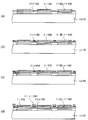
다음으로, 본 실시예에 있어서의 중간층(150)과 보조 음극(160)의 형성 방법에 대하여, 도5 을 이용하여 설명한다. 도5(a) 는, 기판(10)에 형성된 절연층(120) 및 양극(130) 상에, 전술한 유기 재료로 이루어지는 각 기능층을 갖는 유기 EL 소자(140)가 증착에 의해 형성된 상태를 나타내는 단면 개략도이다.Next, the formation method of the intermediate | middle layer 150 and the auxiliary | assistant cathode 160 in a present Example is demonstrated using FIG. 5A shows a state in which an organic EL element 140 having respective functional layers made of the above organic materials is formed on the insulating layer 120 and the anode 130 formed on the
다음으로, 도5(b) 에 나타내는 바와 같이, 서로 인접하는 양극(130)간에 위치하는 유기 EL 소자(140) 상에, 중간층(150)을 마스크 증착에 의해 형성한다. 중간층(150)은 전술한 바와 같이, 무기 재료로 이루어지는 2개의 층으로 구성되어 있고, 우선, 첫번째의 무기 재료층으로서 Ag을 중량 비율 10% 포함하는 MgAg 합금을 마스크 증착하여 퇴적시켜, 막두께 10nm의 MgAg층을 형성한다. 그리고, 다음으로 두번째의 무기 재료층으로서, ITO를 동일한 마스크를 이용하여 증착하고, MgAg층 상에 퇴적시켜, 막두께 100nm의 ITO층을 형성한다.Next, as shown in Fig. 5B, an intermediate layer 150 is formed on the organic EL element 140 positioned between the anodes 130 adjacent to each other by mask deposition. As described above, the intermediate layer 150 is composed of two layers made of an inorganic material. First, an MgAg alloy containing 10% by weight of Ag is deposited by mask deposition as the first inorganic material layer, and the film thickness is 10 nm. The MgAg layer is formed. Then, as the second inorganic material layer, ITO is deposited using the same mask, and deposited on the MgAg layer to form an ITO layer having a film thickness of 100 nm.
다음으로, 도5(c) 에 나타내는 바와 같이, 형성된 중간층(150) 상에, 중간층(150)의 형성에 이용한 동일한 마스크를 이용하여 알루미늄을 증착하고, 두께 300nm의 보조 음극(160)을 형성한다. 이 결과, 보조 음극(160)은, 중간층(150) 상에 바르게 형성되기 때문에, 유기 EL 소자(140)에 직접 형성한 경우에 생기는 벗겨짐도 없고, 중간층(150)을 통하여 유기 EL 소자(140) 상에 확실하게 고정 접착된다.Next, as shown in Fig. 5C, on the formed intermediate layer 150, aluminum is deposited using the same mask used to form the intermediate layer 150 to form an auxiliary cathode 160 having a thickness of 300 nm. . As a result, since the auxiliary cathode 160 is formed correctly on the intermediate layer 150, there is no peeling that occurs when directly formed on the organic EL element 140, and the organic EL element 140 is formed through the intermediate layer 150. It is fixedly adhered to the phase.
다음으로, 도5(d) 에 나타내는 바와 같이, 보조 음극(160) 및 유기 EL 소자(140) 상에, 음극(170)을 증착에 의해 형성한다. 이때, 음극(170)은 보조 음극(160) 상에 겹쳐 증착되기 때문에, 전기적으로 도통이 취해지게 된다. 물론, 보조 음극(160)도 음극(170)도 무기 재료층인 점에서, 양호한 밀착성을 나타낸다.Next, as shown in Fig. 5 (d), the cathode 170 is formed on the auxiliary cathode 160 and the organic EL element 140 by vapor deposition. At this time, since the cathode 170 is deposited on the auxiliary cathode 160, electrical conduction is taken. Of course, since the auxiliary cathode 160 and the cathode 170 are also inorganic material layers, they exhibit good adhesion.
또한, 중간층(150)에 금속 재료를 이용함으로써, 증착 공정시에 생기는 열을 음극(170) 전면에 확산하여 방열하는 확률이 높아지는 점에서, 열응력의 완화에 의해, 중간층(150)의 벗겨짐을 억제할 수 있다.In addition, the use of a metal material for the intermediate layer 150 increases the probability of dissipating and dissipating heat generated during the deposition process to the entire surface of the cathode 170, so that the intermediate layer 150 is peeled off due to relaxation of the thermal stress. It can be suppressed.
그 후, 도4 에 나타낸 바와 같이, 화소 위치에 바르게 배치된 컬러 필터가 기판(10)의 외주 부분에 있어서 접착 고정되어 유기 EL 패널(100)이 완성된다.Thereafter, as shown in FIG. 4, the color filter disposed correctly at the pixel position is adhesively fixed at the outer circumferential portion of the
(제2 실시예)(2nd Example)
다음으로 제2 실시예에 대하여 설명한다. 상기 제1 실시예에서는, 중간층(150)과 보조 음극(160)의 형성 후에 음극(170)을 형성했지만, 제2 실시예는, 중간층(150)의 형성시에 음극(170)을 동시 형성하여, 그 후 보조 음극(160)을 형성하는 것이다.Next, a second embodiment will be described. In the first embodiment, the cathode 170 is formed after the formation of the intermediate layer 150 and the auxiliary cathode 160. In the second embodiment, the cathode 170 is simultaneously formed when the intermediate layer 150 is formed. After that, the auxiliary cathode 160 is formed.
도6 은, 제2 실시예의 보조 음극(160)의 형성 상태를 나타내는 도면으로, 유기 EL 패널(100)의 구조 개략도이다. 도시한 바와 같이, 서로 인접하는 양극(130)간에 존재하는 유기 EL 소자(140) 상에는 중간층(150)이 형성되고, 그 위에 음극(170)이 형성되어 있다. 그리고 음극(170) 상이며, 중간층(150)과 평면적으로 겹치는 위치에 보조 음극(160)이 형성되어 있다.Fig. 6 is a diagram showing the formation state of the auxiliary cathode 160 of the second embodiment, and is a schematic structure of the
본 실시예에서는, 음극(170)은 ITO막이 소정의 두께 형성된 것이다. 또한, 중간층(150)은, 상기 제1 실시예와 동일하게, 전술한 표1 에 있어서의 채용 가능한 재료 중에서 실험 10의 재료 구성을 채용하여 구성된 것이다. 즉, MgAg막(Ag 함유 중량 비율 10%)이 두께 10nm 형성되고, 그 위에, ITO막이 두께 100nm 형성된 것이다. 또한, 보조 음극(160)은, 전기 저항률이 낮은 무기 재료로 형성되고, 여기에서는 알루미늄이 두께 300nm 형성된 것이다. 그리고, 광투과성을 갖는 무기 재료인 ITO로 형성된 음극(170)과 전기적으로 도통하고 있다.In this embodiment, the cathode 170 has an ITO film formed with a predetermined thickness. In addition, similarly to the said 1st Example, the intermediate | middle layer 150 employ | adopts the material structure of
본 실시예에서는, 중간층(150)을 구성하는 층의 1개와, 음극(170)이, 이러한 동일한 무기 재료 ITO로 형성되는 경우는, 각각의 막두께를 동일하게 함으로써, 이들을 동시에 형성할 수 있게 한다. 즉, 음극(170)의 ITO막의 두께를, 중간층(150)을 구성하는 ITO막의 두께와 동일한 100nm로 한다. 이 결과, 중간층(150)을 구성하는 ITO막의 형성과 동시에 음극(170)을 형성할 수 있기 때문에, 제1 실시예에 비하여 형성 공정이 짧아진다.In the present embodiment, when one of the layers constituting the intermediate layer 150 and the cathode 170 are formed of the same inorganic material ITO, the respective film thicknesses are made the same so that they can be formed simultaneously. . That is, the thickness of the ITO film of the cathode 170 is 100 nm which is the same as the thickness of the ITO film constituting the intermediate layer 150. As a result, since the cathode 170 can be formed simultaneously with the formation of the ITO film constituting the intermediate layer 150, the formation process is shorter than in the first embodiment.
이와 같이, 본 실시예에서는, 유기 EL 소자(140)에 대하여 밀착성이 높은 중간층(150)을 형성할 때, 동시에 음극(170)을 형성한다. 이 결과, 본래는 유기 재료에 대하여 벗겨지기 쉬운 알루미늄으로 형성된 전기 저항이 낮은 보조 음극(160)을, 중간층(150)을 통함으로써, 유기 재료로 형성된 비발광 영역에 벗겨지는 일 없이 형성할 수 있다. 그리고, ITO로 형성된 전기 저항이 높은 음극(170)과, 전기 저항이 낮은 보조 음극(160)이, 전기적으로 접속됨으로써, 각 화소에 있어서의 음극(170)의 전위차가 억제된다. 따라서, 양극(130)으로부터 유기 EL 소자(140)에 흐르는 전류는 억제되지 않기 때문에, 유기 EL 소자(140)의 발광 휘도가 저하되지 않고, RGB의 각 화소의 발광 휘도에 의해 바르게 컬러 화상을 표시하는 신뢰성이 높은 유기 EL 패널(100)을 제공할 수 있다.As described above, in the present embodiment, the cathode 170 is formed at the same time when the intermediate layer 150 having high adhesion to the organic EL element 140 is formed. As a result, the auxiliary cathode 160, which is originally made of aluminum, which is easily peeled off against the organic material, can be formed without passing through the non-light emitting region formed of the organic material by passing through the intermediate layer 150. . The potential difference between the cathode 170 having high electrical resistance and the auxiliary cathode 160 having low electrical resistance is electrically connected to each other to suppress the potential difference between the cathodes 170 in each pixel. Therefore, since the current flowing from the anode 130 to the organic EL element 140 is not suppressed, the light emission luminance of the organic EL element 140 does not decrease, and the color image is correctly displayed by the light emission luminance of each pixel of RGB. The highly reliable
또한, 제2 실시예의 경우는, 중간층(150)을 구성하는 ITO막과, 음극(170)을 형성하는 ITO막과는, 동일한 1개의 막층이 되지만, 중간층(150)을 구성하는 MgAg막과 평면적으로 겹치는 부분이 중간층(150)을 구성하는 ITO막이 된다. 따라서, 제2 실시예에서는, 보조 음극(160)과 음극(170)과는, 중간층(150)을 구성하는 ITO막을 통하여 전기적으로 접속되게 된다.In the second embodiment, the ITO film constituting the intermediate layer 150 and the ITO film constituting the cathode 170 are the same one film layer, but the MgAg film constituting the intermediate layer 150 is planar. The overlapped portions become the ITO film constituting the intermediate layer 150. Therefore, in the second embodiment, the auxiliary cathode 160 and the cathode 170 are electrically connected through the ITO film constituting the intermediate layer 150.
다음으로, 본 실시예에 있어서의 중간층(150)과 보조 음극(160)의 형성 방법에 대하여, 도7 을 이용하여 설명한다. 도7(a) 는, 기판(10)에 형성된 절연층(120) 및 양극(130) 상에, 전술한 유기 재료로 이루어지는 각 기능층을 갖는 유기 EL 소자(140)가 증착에 의해 형성된 상태를 나타내는 단면 개략도이다.Next, the formation method of the intermediate | middle layer 150 and the auxiliary cathode 160 in a present Example is demonstrated using FIG. FIG. 7A shows a state in which an organic EL element 140 having respective functional layers made of the above organic materials is formed on the insulating layer 120 and the anode 130 formed on the
다음으로, 도7(b) 에 나타내는 바와 같이, 서로 인접하는 양극(130)간에 위치하는 유기 EL 소자(140) 상에, 중간층(150)을 마스크 증착에 의해 형성한다. 중간층(150)은 전술한 바와 같이, 무기 재료로 이루어지는 2개의 층으로 구성되어 있고, 우선, 첫번째의 무기 재료층으로서, Ag을 10% 중량 성분 포함하는 Mg을 마스크 증착하여 퇴적시켜, 막두께 10nm의 MgAg층을 형성한다.Next, as shown in Fig. 7B, an intermediate layer 150 is formed on the organic EL element 140 positioned between the anodes 130 adjacent to each other by mask deposition. As described above, the intermediate layer 150 is composed of two layers made of an inorganic material. First, as the first inorganic material layer, Mg containing 10% by weight of Ag is deposited by mask deposition, and the film thickness is 10 nm. The MgAg layer is formed.
다음으로, 도7(c) 에 나타내는 바와 같이, 형성된 중간층(150)의 첫번째의 층인 MgAg층의 위와, 유기 EL 소자(140)의 위에, ITO를 증착하고, 막두께 100nm의 ITO층을 형성한다. 이 형성 공정에 의해, 중간층(150)의 두번째의 무기 재료층과 음극(170)이 동시에 형성되게 된다.Next, as shown in Fig. 7C, ITO is deposited on the MgAg layer which is the first layer of the formed intermediate layer 150 and on the organic EL element 140 to form an ITO layer having a film thickness of 100 nm. . By this forming process, the second inorganic material layer of the intermediate layer 150 and the cathode 170 are simultaneously formed.
다음으로, 도7(d) 에 나타내는 바와 같이, 중간층(150)의 첫번째층이 되는 MgAg층의 형성에 이용한 동일한 마스크를 이용하여 알루미늄을 증착하고, 두께 300nm의 보조 음극(160)을 형성한다. 이 결과, 보조 음극(160)은, 중간층(150) 상에 바르게 형성되기 때문에, 유기 EL 소자(140)에 직접 형성한 경우에 생기는 벗겨짐도 없고, 중간층(150)을 통하여 유기 EL 소자(140) 상에 확실하게 고정 접착된다.Next, as shown in Fig. 7 (d), aluminum is deposited using the same mask used for forming the MgAg layer serving as the first layer of the intermediate layer 150 to form an auxiliary cathode 160 having a thickness of 300 nm. As a result, since the auxiliary cathode 160 is formed correctly on the intermediate layer 150, there is no peeling that occurs when directly formed on the organic EL element 140, and the organic EL element 140 is formed through the intermediate layer 150. It is fixedly adhered to the phase.
또한, 상기 제1 실시예와 동일하게, 중간층(150)에 금속 재료를 이용함으로써, 증착 공정시에 생기는 열을 음극(170) 전면에 확산하여 방열하는 확률이 높아지는 점에서, 열응력의 완화에 의해, 중간층(150)의 벗겨짐을 억제할 수 있다. 또한, 추가로 보조 음극(160)을 2층막으로 함으로써, 음극(170)과의 밀착성을 높이는 것이 가능하다. 구체적으로는, 보조 음극(160)의 아래에 MgAg막을 30nm 정도 보조 음극을 형성하는 증착 마스크로 성막함으로써 실현할 수 있다.In addition, similarly to the first embodiment, the use of a metal material for the intermediate layer 150 increases the probability of dissipating and dissipating heat generated during the deposition process to the entire surface of the cathode 170, thereby reducing thermal stress. As a result, peeling of the intermediate layer 150 can be suppressed. In addition, by making the auxiliary cathode 160 a two-layer film, it is possible to improve the adhesion with the cathode 170. Specifically, this can be achieved by forming an MgAg film under the auxiliary cathode 160 with a deposition mask that forms an auxiliary cathode on the order of 30 nm.
그 후, 도6 에 나타낸 바와 같이, 화소 위치에 바르게 배치된 컬러 필터가 기판(10)의 외주 부분에 있어서 접착 고정되어 유기 EL 패널(100)이 완성된다.Thereafter, as shown in Fig. 6, the color filter disposed correctly at the pixel position is adhesively fixed at the outer peripheral portion of the
이상, 본 발명에 대하여, 2개의 실시예를 이용하여 설명했지만, 본 발명은 이러한 실시예에 조금도 한정되는 것이 아니고, 본 발명의 취지를 일탈하지 않는 범위 내에 있어서 여러가지 형태로 실시할 수 있는 것은 물론이다. 이하 변형예를 들어 설명한다.As mentioned above, although this invention was demonstrated using two Example, this invention is not limited to these Examples at all and can be implemented in various forms within the range which does not deviate from the meaning of this invention. to be. A modification is given below.
(제1 변형예)(First modification)
상기 실시예는, 유기 EL 소자는 발광광이 백색광이며, 컬러 필터로 RGB의 각 색으로 변환하여 사출하는 유기 EL 패널에 대하여 실시하는 것으로서 설명했지만, 이것에 한정하는 것이 아닌 것은 물론이다. 예를 들면, 유기 EL 소자가, 각각의 RGB가 다른 색을 발광하는 유기 EL 패널이여도 실시하는 것이 가능하다. 이 변형예에 대하여 도8 을 이용하여 설명한다.In the above embodiment, the organic EL element is a light emitted from white light, and the organic EL element is described as being implemented with respect to an organic EL panel which is converted into each color of RGB and is emitted, but it is a matter of course that the organic EL element is not limited thereto. For example, it is possible to implement even if the organic EL element is an organic EL panel in which each RGB emits a different color. This modification is demonstrated using FIG.
도8 은, 본 변형예의 유기 EL 패널의 구조를 나타내는 개략도이다. 도시하는 바와 같이, 기판(10) 상에 형성된 양극(130)의 주위에는, 적어도 표면이 도전성을 가지지 않는 유기 재료로 이루어지는 격벽이 형성되고, 이 격벽에 의해 둘러싸인 영역에, 발광색이 다른 R 발광층, G 발광층, B 발광층이 되는 유기 EL 소자가 형성되어 있다. 그리고, 격벽을 포함하여 각 발광층 전체를 덮도록 음극(170)이 형성되어 있다. 따라서, 양극(130)과 음극(170)과의 사이에 소정의 전류를 흘림으로써, 각각의 유기 EL 소자는, 발광층에 따른 RGB의 발광색을 사출하여, 각각 R 화소, G 화소, B 화소가 된다.8 is a schematic view showing the structure of the organic EL panel of the present modification. As shown, around the anode 130 formed on the board |
본 변형예에서는, 발광층은, RGB의 각 색을 나타내는 형광 재료를 용질(溶質; solute)로 하는 기능액 등, 유기 EL 소자를 구성하는 기능층을 형성하기 위한 기능액을, 격벽으로 둘러싸인 영역으로 분사하고, 진공 건조 등의 열처리를 행하여, 소정의 두께의 막을 형성한 것이다. 따라서, 격벽은, 분사된 기능액이 격벽으로 둘러싸인 영역에 머물도록 필요에 따라 표면에 발액(lyophobic) 처리를 행할 수 있도록, 통상, 유기 재료(예를 들면, 폴리이미드 수지나 아크릴 수지)로 형성되어 있는 것이다. 또한, 격벽은 포토리소에 의한 에칭(photolithographic etching)에 의해 형성된다.In the present modification, the light emitting layer includes a functional liquid for forming a functional layer constituting an organic EL element, such as a functional liquid containing solutes a fluorescent material representing each color of RGB, in a region surrounded by a partition wall. It sprays and heat-processes, such as vacuum drying, and forms the film | membrane of predetermined thickness. Therefore, the partition is usually formed of an organic material (for example, a polyimide resin or an acrylic resin) so that the lyophobic treatment may be performed on the surface as necessary so that the injected functional liquid stays in an area surrounded by the partition. It is. In addition, the partition wall is formed by photolithographic etching.
이러한 구성을 갖는 유기 EL 패널에 있어서, 음극(170)에 생기는 전위차를 억제하기 위해, 전기 저항이 낮은 보조 음극(160)을 형성하는 경우는, 격벽이 비발광 영역으로 되기 때문에, 격벽 상에 형성된다. 따라서, 유기 재료에 대하여 밀착성이 낮은 보조 음극(160)을 형성하기 위해, 격벽 상에 우선 유기 재료에 대하여 밀착성이 높은 중간층(150)을 마스크 증착에 의해 형성한다. 그 후, 동일한 마스크를 이용하여 보조 음극(160)을 형성하고, 보조 음극(160)과 전기적인 접속을 취하기 위해, 보조 음극(160)과 각 발광층을 덮도록 음극(170)을 형성하는 것이다. 물론, 상기 제2 실시예와 같이, 중간층(150)을 구성하는 1개의 층을 형성할 때에, 동시에 음극(170)을 형성하는 것으로 해도 좋다.In the organic EL panel having such a structure, in order to suppress the potential difference occurring in the cathode 170, when the auxiliary cathode 160 having a low electrical resistance is formed, the partition wall becomes a non-light emitting region, so that it is formed on the partition wall. do. Therefore, in order to form the auxiliary cathode 160 having low adhesion to the organic material, an intermediate layer 150 having high adhesion to the organic material is first formed on the partition wall by mask deposition. Thereafter, the auxiliary cathode 160 is formed using the same mask, and the cathode 170 is formed to cover the auxiliary cathode 160 and each light emitting layer in order to make electrical connection with the auxiliary cathode 160. Of course, as in the second embodiment, when forming one layer constituting the intermediate layer 150, the cathode 170 may be formed at the same time.
본 변형예에 의하면, 유기 재료로 이루어지는 격벽에 대하여 밀착성이 높은 중간층(150)을 형성한다. 이 결과, 유기 재료에 대하여 밀착성이 낮은 보조 음극(160)을, 중간층(150)을 통하여 벗겨지는 일 없이 형성할 수 있다. 그리고, 전기 저항이 높은 음극(170)과 전기 저항이 낮은 보조 음극(160)이 전기적으로 접속됨으로써, 각 화소에 있어서의 음극(170)의 전위차가 억제된다. 따라서, 양극(130)으로부터 유기 EL 소자(140)에 흐르는 전류는 억제되지 않기 때문에, 유기 EL 소자(140)의 발광 휘도가 저하되지 않고, RGB의 각 화소의 발광 휘도에 의해 바르게 컬러 화상을 표시할 수 있다.According to this modification, the intermediate | middle layer 150 with high adhesiveness with respect to the partition which consists of organic materials is formed. As a result, the auxiliary cathode 160 having low adhesion to the organic material can be formed without being peeled off through the intermediate layer 150. The potential difference between the cathode 170 in each pixel is suppressed by electrically connecting the cathode 170 having a high electrical resistance and the auxiliary cathode 160 having a low electrical resistance. Therefore, since the current flowing from the anode 130 to the organic EL element 140 is not suppressed, the light emission luminance of the organic EL element 140 does not decrease, and the color image is correctly displayed by the light emission luminance of each pixel of RGB. can do.
(제2 변형예)(Second modification)
상기 실시예에서는, 상기 제1 변형예에 나타낸 바와 같은 격벽이, 서로 인접하는 양극(130)간에 있어서 존재하지 않는 유기 EL 패널로서 설명했지만, 이것에 한정되지 않고, 격벽을 형성하는 것으로 해도 좋다. 실제로, 유기 EL 소자를 형성하는 경우, 마스크를 사용하여 유기 재료를 증착한다. 이때 마스크와 증착면과의 사이에 간극(gap)이 존재하지 않는 경우, 사용하는 마스크에 부착한 미소(微小) 이물질이 화소 부분에 전사되기 쉬워져, 화소 결함이 발생해 버린다. 그래서, 소정의 높이를 갖는 격벽을 형성함으로써, 화소 결함을 억제할 수 있는 것이다. 이 변형예에 대하여 도9 를 이용하여 설명한다.In the said embodiment, although the partition as shown in the said 1st modification demonstrated as an organic EL panel which does not exist between the anodes 130 adjacent to each other, it is not limited to this, You may form a partition. In fact, when forming an organic EL element, a mask is used to deposit an organic material. At this time, when there is no gap between the mask and the vapor deposition surface, fine foreign matter adhering to the mask to be used is easily transferred to the pixel portion, resulting in pixel defects. Therefore, pixel defects can be suppressed by forming a partition having a predetermined height. This modification is demonstrated using FIG.
도9 는, 본 변형예의 유기 EL 패널의 구조를 나타내는 개략도이다. 또한 컬러 필터는 생략하고 있다. 도시한 바와 같이, 절연층(120) 상에 형성된 양극(130)의 주위에는, 적어도 표면이 도전성을 가지지 않는 유기 재료로 이루어지는 격벽이 형성되고, 이 격벽 및 양극(130)을 포함하는 모든 영역에 걸쳐, 백색광을 발광하는 유기 EL 소자(140)가 형성되어 있다. 그리고, 유기 EL 소자(140) 전체를 덮도록 음극(170)이 형성되어 있다.9 is a schematic view showing the structure of the organic EL panel of the present modification. In addition, the color filter is abbreviate | omitted. As shown in the figure, around the anode 130 formed on the insulating layer 120, a partition wall formed of an organic material whose surface is not conductive at least is formed, and in all regions including the partition wall and the anode 130. On the other hand, the organic EL element 140 which emits white light is formed. And the cathode 170 is formed so that the whole organic electroluminescent element 140 may be covered.
본 변형예에서는, 이러한 구성을 갖는 유기 EL 패널에 있어서, 음극(170)에 생기는 전위차를 억제하기 위해, 전기 저항이 낮은 보조 음극(160)을 형성하는 경우, 비발광 영역이 되는 격벽 상에 형성하게 된다. 따라서, 보조 음극(160)을 형성하기 위해, 격벽 상에 우선 유기 EL 소자(140)를 형성하는 유기 재료에 대하여 밀착성이 높은 중간층(150)을 마스크 증착에 의해 형성한다. 그 후, 동일한 마스크를 이용하여 보조 음극(160)을 형성하고, 보조 음극(160)과 전기적인 접속을 취하기 위해, 보조 음극(160)과 각 발광층을 덮도록 음극(170)을 형성하는 것이다.In the present modified example, in the organic EL panel having such a configuration, in order to suppress the potential difference generated in the cathode 170, when the auxiliary cathode 160 having low electrical resistance is formed, it is formed on the partition that becomes the non-light emitting region. Done. Therefore, in order to form the auxiliary cathode 160, an intermediate layer 150 having high adhesion to the organic material for forming the organic EL element 140 on the partition wall is first formed by mask deposition. Thereafter, the auxiliary cathode 160 is formed using the same mask, and the cathode 170 is formed to cover the auxiliary cathode 160 and each light emitting layer in order to make electrical connection with the auxiliary cathode 160.
본 변형예에 의하면, 유기 EL 소자(140)에 대하여 밀착성이 높은 중간층(150)을 형성한다. 이 결과, 유기 재료에 대하여 밀착성이 나쁜 보조 음극(160)을, 중간층(150)을 통하여 벗겨지는 일 없이 형성할 수 있다. 그리고, 전기 저항이 높은 음극(170)과 전기 저항이 낮은 보조 음극(160)이 전기적으로 접속됨으로써, 각 화소에 있어서의 음극(170)의 전위차가 억제된다. 따라서, 양극(130)으로부터 유기 EL 소자(140)에 흐르는 전류는 억제되지 않기 때문에, 유기 EL 소자(140)의 발광 휘도가 저하되지 않고, RGB의 각 화소의 발광 휘도에 의해 바르게 컬러 화상을 표시할 수 있다.According to this modification, the intermediate | middle layer 150 with high adhesiveness with respect to the organic electroluminescent element 140 is formed. As a result, the auxiliary cathode 160 having poor adhesion to the organic material can be formed without peeling off through the intermediate layer 150. The potential difference between the cathode 170 in each pixel is suppressed by electrically connecting the cathode 170 having a high electrical resistance and the auxiliary cathode 160 having a low electrical resistance. Therefore, since the current flowing from the anode 130 to the organic EL element 140 is not suppressed, the light emission luminance of the organic EL element 140 does not decrease, and the color image is correctly displayed by the light emission luminance of each pixel of RGB. can do.
(그 외의 변형예)(Other modifications)
상기 실시예에서는, 중간층에 사용할 수 있는 무기 재료에 대하여, 금속 혹은 합금을 이용하는 것으로 했지만, 특별히 이것에 한정하는 것이 아닌 것은 물론이다. 예를 들면, 금속 재료 이외에 칼슘(Ca)을 이용해도 좋다. 또한 합금 재료 이외에 산화 실리콘이나 질화 실리콘을 이용해도 좋다. 또한, 합금에 대해서도, 금속 산화물 이외에 금속 질화물을 이용해도 좋다. 이들의 무기 재료는, 전술한 표1 에는 나타내고 있지 않지만, 상기 실시예와 동일하게 유기 재료에 대한 밀착성을 조사한 테스트 결과로부터, 밀착성의 개선 효과를 얻는 것이 가능한 재료이다.In the said Example, although the metal or alloy was used for the inorganic material which can be used for an intermediate | middle layer, it does not need to limit to this in particular. For example, calcium (Ca) may be used in addition to the metal material. In addition to the alloying material, silicon oxide or silicon nitride may be used. Moreover, also about an alloy, you may use metal nitride other than a metal oxide. Although these inorganic materials are not shown in Table 1 mentioned above, they are the materials which can obtain the improvement effect of adhesiveness from the test result which investigated the adhesiveness with respect to organic material similarly to the said Example.
또한, 상기 실시예에서는, 중간층을 2층의 무기 재료층으로 했지만, 특별히 이것에 한정하는 것이 아닌 것은 물론이다. 예를 들면, 3층으로 해도 좋고, 1층으로 해도 좋다. 1층으로 한 경우는, 기본적으로 중간층의 형성에 있어서 음극을 동시에 형성하는 것은 곤란하지만, 예를 들면 동일한 무기 재료로서 막두께만이 다른 경우는, 재료를 변경하는 일 없이 마스크를 교환할 뿐으로 연속하여 증착할 수 있는 가능성이 있기 때문에, 성막 공정이 용이해진다.In addition, in the said Example, although the intermediate | middle layer was made into two inorganic material layers, of course, it does not limit to this in particular. For example, it may be three layers or may be one layer. In the case of one layer, it is difficult to form the cathode at the same time in the formation of the intermediate layer. However, in the case where only the film thickness is different as the same inorganic material, for example, only the mask is replaced without changing the material. Since there is a possibility of vapor deposition by vapor deposition, the film forming step becomes easy.
또한, 상기 실시예에서는, 표시 소자의 발광광의 사출 방향을 음극측으로 하는 톱 이미션 방식인 것으로서 설명했지만, 이것에 한정하지 않고, 표시 소자의 발광광의 사출 방향을 기판측에도 사출하는 방식인 것으로 해도 좋다. 이 경우, 반사층을 형성하지 않고, 기판 및 양극의 재료는 광투과성을 갖는 재료(예를 들면, 유리나 ITO)로 하면 좋다. 또한, TFT 등의 구동 소자는, 발광 소자와 평면적으로 겹치게 할 수 없기 때문에, 기판과 표시 소자와의 사이에 디바이스층이 개재하지 않게 된다.In addition, in the said Example, it demonstrated as what is the top emission system which makes the emission direction of the light emission of a display element into a cathode side, It is not limited to this, You may make it the system which injects the emission direction of the emission light of a display element also to a board | substrate side. . In this case, the material of the substrate and the anode may be made of a material having light transmittance (for example, glass or ITO) without forming a reflective layer. In addition, since a driving element such as a TFT cannot be overlapped with the light emitting element in plan view, a device layer is not interposed between the substrate and the display element.
도1 은 유기 EL 패널의 전체의 레이아웃을, 회로 구성과 함께 나타낸 개략도이다.1 is a schematic diagram showing an entire layout of an organic EL panel together with a circuit configuration.
도2(a) 는 유기 EL 패널에 있어서의 RGB의 각 화소에 대한 구성을 개략적으로 나타내는 평면도이며, 도2(b) 는 그 개략 단면도이다.Fig. 2A is a plan view schematically showing the configuration of each pixel of RGB in the organic EL panel, and Fig. 2B is a schematic sectional view thereof.
도3 은 양극과 평면적으로 겹치지 않는 위치에 형성하는 보조 음극을 나타내는 개략 평면도이다.Fig. 3 is a schematic plan view showing an auxiliary cathode formed at a position where the anode does not overlap with the plane.
도4 는 제1 실시예의 보조 음극의 형성 상태를 나타내는 유기 EL 패널의 구조 개략도이다.Fig. 4 is a structural schematic diagram of an organic EL panel showing the formation state of the auxiliary cathode of the first embodiment.
도5(a)∼(d) 는 제1 실시예에 있어서의 중간층과 보조 음극의 형성 방법을 설명하는 설명도이다.5A to 5D are explanatory views for explaining a method for forming an intermediate layer and an auxiliary cathode in the first embodiment.
도6 은 제2 실시예의 보조 음극의 형성 상태를 나타내는 유기 EL 패널의 구조 개략도이다.6 is a structural schematic diagram of an organic EL panel showing a state of formation of an auxiliary cathode of a second embodiment.
도7(a)∼(d) 는 제2 실시예에 있어서의 중간층과 보조 음극의 형성 방법을 설명하는 설명도이다.7 (a) to 7 (d) are explanatory views for explaining a method for forming the intermediate layer and the auxiliary cathode in the second embodiment.
도8 은 제1 변형예의 유기 EL 패널의 구조를 나타내는 개략도이다.8 is a schematic view showing the structure of the organic EL panel of the first modification.
도9 는 제2 변형예의 유기 EL 패널의 구조를 나타내는 개략도이다.9 is a schematic view showing the structure of an organic EL panel of a second modification.
(도면의 주요 부분에 대한 부호의 설명)(Explanation of symbols for the main parts of the drawing)
10 : 기판10: substrate
11 : 주사 구동회로11: scan driving circuit
12 : 데이터 구동회로12: data driving circuit
13 : 급전 단자13: power supply terminal
14, 15 : TFT14, 15: TFT
16 : 유지 용량16: holding capacity
20 : 디바이스층20: device layer
100 : 유기 EL 패널100: organic EL panel
110 : 반사층110: reflective layer
120 : 절연층120: insulation layer
130 : 양극130: anode
140 : 유기 EL 소자140: organic EL device
150 : 중간층150: middle layer
160 : 보조 음극160: auxiliary cathode
170 : 음극170: cathode
Claims (8)
Applications Claiming Priority (2)
| Application Number | Priority Date | Filing Date | Title |
|---|---|---|---|
| JPJP-P-2008-002921 | 2008-01-10 | ||
| JP2008002921A JP5056420B2 (en) | 2008-01-10 | 2008-01-10 | Organic EL panel and manufacturing method thereof |
Publications (1)
| Publication Number | Publication Date |
|---|---|
| KR20090077690A true KR20090077690A (en) | 2009-07-15 |
Family
ID=40850052
Family Applications (1)
| Application Number | Title | Priority Date | Filing Date |
|---|---|---|---|
| KR1020090000294A Withdrawn KR20090077690A (en) | 2008-01-10 | 2009-01-05 | Organic EL panel and its manufacturing method |
Country Status (5)
| Country | Link |
|---|---|
| US (1) | US20090179558A1 (en) |
| JP (1) | JP5056420B2 (en) |
| KR (1) | KR20090077690A (en) |
| CN (1) | CN101483188B (en) |
| TW (1) | TW200948182A (en) |
Families Citing this family (8)
| Publication number | Priority date | Publication date | Assignee | Title |
|---|---|---|---|---|
| JP2012049034A (en) * | 2010-08-27 | 2012-03-08 | Nakanuma Art Screen Kk | Inorganic el light-emitting element, resin molded article, transfer sheet, manufacturing method of transfer sheet, and manufacturing method of resin molded article |
| JP2014509442A (en) * | 2011-03-22 | 2014-04-17 | オーシャンズ キング ライティング サイエンス アンド テクノロジー シーオー.,エルティーディー | Organic electroluminescent device and conductive substrate thereof |
| US10601033B2 (en) | 2017-09-29 | 2020-03-24 | International Business Machines Corporation | High-performance rechargeable batteries having a spalled and textured cathode layer |
| US20190103637A1 (en) * | 2017-09-29 | 2019-04-04 | International Business Machines Corporation | Methods of forming rechargeable battery stacks containing a spalled cathode material |
| US10622636B2 (en) | 2017-09-29 | 2020-04-14 | International Business Machines Corporation | High-capacity rechargeable battery stacks containing a spalled cathode material |
| CN108022962A (en) * | 2017-11-30 | 2018-05-11 | 深圳市华星光电技术有限公司 | Display panel and its manufacture method |
| CN111509138A (en) * | 2020-04-27 | 2020-08-07 | 合肥鑫晟光电科技有限公司 | Display panel and method of making the same |
| CN114171362B (en) * | 2022-02-09 | 2022-05-24 | 之江实验室 | Particle transfer device and application |
Family Cites Families (16)
| Publication number | Priority date | Publication date | Assignee | Title |
|---|---|---|---|---|
| JP4470241B2 (en) * | 1999-08-25 | 2010-06-02 | ソニー株式会社 | Organic EL display and manufacturing method thereof |
| TW511298B (en) * | 1999-12-15 | 2002-11-21 | Semiconductor Energy Lab | EL display device |
| JP4434411B2 (en) * | 2000-02-16 | 2010-03-17 | 出光興産株式会社 | Active drive type organic EL light emitting device and manufacturing method thereof |
| US6841932B2 (en) * | 2001-03-08 | 2005-01-11 | Xerox Corporation | Display devices with organic-metal mixed layer |
| US7288887B2 (en) * | 2001-03-08 | 2007-10-30 | Lg.Philips Lcd Co. Ltd. | Devices with multiple organic-metal mixed layers |
| JP2002343562A (en) * | 2001-05-11 | 2002-11-29 | Pioneer Electronic Corp | Light emitting display device and method of manufacturing the same |
| JP4627966B2 (en) * | 2002-01-24 | 2011-02-09 | 株式会社半導体エネルギー研究所 | Light emitting device and manufacturing method thereof |
| SG143063A1 (en) * | 2002-01-24 | 2008-06-27 | Semiconductor Energy Lab | Light emitting device and method of manufacturing the same |
| US7015639B2 (en) * | 2002-10-22 | 2006-03-21 | Osram Opto Semiconductors Gmbh | Electroluminescent devices and method of making transparent cathodes |
| JP2005019211A (en) * | 2003-06-26 | 2005-01-20 | Casio Comput Co Ltd | EL display panel and method of manufacturing EL display panel |
| JP2005302308A (en) * | 2004-04-06 | 2005-10-27 | Seiko Epson Corp | Organic EL display device and manufacturing method thereof |
| JP4367346B2 (en) * | 2005-01-20 | 2009-11-18 | セイコーエプソン株式会社 | ELECTRO-OPTICAL DEVICE, MANUFACTURING METHOD THEREOF, AND ELECTRONIC DEVICE |
| JP4513777B2 (en) * | 2005-11-14 | 2010-07-28 | セイコーエプソン株式会社 | LIGHT EMITTING DEVICE AND ELECTRONIC DEVICE |
| JP2007165215A (en) * | 2005-12-16 | 2007-06-28 | Seiko Epson Corp | Method for manufacturing electroluminescence device |
| JP4673279B2 (en) * | 2005-12-20 | 2011-04-20 | 三星モバイルディスプレイ株式會社 | Organic light emitting display device and method for manufacturing the same |
| JP2007335412A (en) * | 2007-08-03 | 2007-12-27 | Idemitsu Kosan Co Ltd | Multicolor light emitting device and manufacturing method thereof |
-
2008
- 2008-01-10 JP JP2008002921A patent/JP5056420B2/en active Active
- 2008-12-29 US US12/345,116 patent/US20090179558A1/en not_active Abandoned
-
2009
- 2009-01-05 KR KR1020090000294A patent/KR20090077690A/en not_active Withdrawn
- 2009-01-08 CN CN2009100030330A patent/CN101483188B/en active Active
- 2009-01-09 TW TW098100636A patent/TW200948182A/en unknown
Also Published As
| Publication number | Publication date |
|---|---|
| CN101483188B (en) | 2012-07-04 |
| TW200948182A (en) | 2009-11-16 |
| JP5056420B2 (en) | 2012-10-24 |
| JP2009164068A (en) | 2009-07-23 |
| US20090179558A1 (en) | 2009-07-16 |
| CN101483188A (en) | 2009-07-15 |
Similar Documents
| Publication | Publication Date | Title |
|---|---|---|
| US7427783B2 (en) | Top emission organic light emitting diode display using auxiliary electrode to prevent voltage drop of upper electrode | |
| US8004178B2 (en) | Organic light emitting diode display with a power line in a non-pixel region | |
| KR102614612B1 (en) | Flat Panel Display Connecting Front Side to Rear Side of Substrate Using Through Hole | |
| US8581273B2 (en) | Organic EL device | |
| CN111164666B (en) | Display device | |
| JP2003257667A (en) | Organic electroluminescent device and method of manufacturing the same | |
| JP6872343B2 (en) | Display device and manufacturing method of display device | |
| KR102894812B1 (en) | Light emitting display device | |
| JP5056420B2 (en) | Organic EL panel and manufacturing method thereof | |
| JP2020109452A (en) | Display device and manufacturing method for display device | |
| KR20190026351A (en) | Eletroluminescence display device | |
| CN113170551A (en) | Display device and method for manufacturing the same | |
| KR20250149922A (en) | Light Emitting Diodes Display Apparatus | |
| US20240222586A1 (en) | Light-Emitting Display Device | |
| KR20260025117A (en) | Display panel | |
| US20260020450A1 (en) | Display apparatus | |
| KR20180063627A (en) | Organic light emitting display device | |
| CN111819908A (en) | Organic EL Display Device | |
| US12598868B2 (en) | Display device | |
| US20220199955A1 (en) | Display device and manufactring method thereof | |
| KR102869030B1 (en) | Light Emitting Diodes Display Apparatus | |
| KR102795076B1 (en) | Organic light emitting displays device | |
| KR20120134043A (en) | Organic el device | |
| US20240260323A1 (en) | Light emitting display device and method of manufacturing same | |
| JP2020027883A (en) | Organic EL display device and method of manufacturing organic EL display device |
Legal Events
| Date | Code | Title | Description |
|---|---|---|---|
| PA0109 | Patent application |
St.27 status event code: A-0-1-A10-A12-nap-PA0109 |
|
| PG1501 | Laying open of application |
St.27 status event code: A-1-1-Q10-Q12-nap-PG1501 |
|
| PC1203 | Withdrawal of no request for examination |
St.27 status event code: N-1-6-B10-B12-nap-PC1203 |
|
| WITN | Application deemed withdrawn, e.g. because no request for examination was filed or no examination fee was paid | ||
| R18-X000 | Changes to party contact information recorded |
St.27 status event code: A-3-3-R10-R18-oth-X000 |
|
| P22-X000 | Classification modified |
St.27 status event code: A-2-2-P10-P22-nap-X000 |
|
| P22-X000 | Classification modified |
St.27 status event code: A-2-2-P10-P22-nap-X000 |
|
| P22-X000 | Classification modified |
St.27 status event code: A-2-2-P10-P22-nap-X000 |
|
| P22-X000 | Classification modified |
St.27 status event code: A-2-2-P10-P22-nap-X000 |