KR20090106162A - 유기 발광 표시장치 및 그 구동방법 - Google Patents
유기 발광 표시장치 및 그 구동방법 Download PDFInfo
- Publication number
- KR20090106162A KR20090106162A KR1020080031705A KR20080031705A KR20090106162A KR 20090106162 A KR20090106162 A KR 20090106162A KR 1020080031705 A KR1020080031705 A KR 1020080031705A KR 20080031705 A KR20080031705 A KR 20080031705A KR 20090106162 A KR20090106162 A KR 20090106162A
- Authority
- KR
- South Korea
- Prior art keywords
- transistor
- light emitting
- organic light
- scan signal
- scan
- Prior art date
- Legal status (The legal status is an assumption and is not a legal conclusion. Google has not performed a legal analysis and makes no representation as to the accuracy of the status listed.)
- Ceased
Links
Images




Classifications
-
- G—PHYSICS
- G09—EDUCATION; CRYPTOGRAPHY; DISPLAY; ADVERTISING; SEALS
- G09G—ARRANGEMENTS OR CIRCUITS FOR CONTROL OF INDICATING DEVICES USING STATIC MEANS TO PRESENT VARIABLE INFORMATION
- G09G3/00—Control arrangements or circuits, of interest only in connection with visual indicators other than cathode-ray tubes
- G09G3/20—Control arrangements or circuits, of interest only in connection with visual indicators other than cathode-ray tubes for presentation of an assembly of a number of characters, e.g. a page, by composing the assembly by combination of individual elements arranged in a matrix no fixed position being assigned to or needed to be assigned to the individual characters or partial characters
- G09G3/22—Control arrangements or circuits, of interest only in connection with visual indicators other than cathode-ray tubes for presentation of an assembly of a number of characters, e.g. a page, by composing the assembly by combination of individual elements arranged in a matrix no fixed position being assigned to or needed to be assigned to the individual characters or partial characters using controlled light sources
- G09G3/30—Control arrangements or circuits, of interest only in connection with visual indicators other than cathode-ray tubes for presentation of an assembly of a number of characters, e.g. a page, by composing the assembly by combination of individual elements arranged in a matrix no fixed position being assigned to or needed to be assigned to the individual characters or partial characters using controlled light sources using electroluminescent panels
-
- G—PHYSICS
- G09—EDUCATION; CRYPTOGRAPHY; DISPLAY; ADVERTISING; SEALS
- G09G—ARRANGEMENTS OR CIRCUITS FOR CONTROL OF INDICATING DEVICES USING STATIC MEANS TO PRESENT VARIABLE INFORMATION
- G09G3/00—Control arrangements or circuits, of interest only in connection with visual indicators other than cathode-ray tubes
- G09G3/20—Control arrangements or circuits, of interest only in connection with visual indicators other than cathode-ray tubes for presentation of an assembly of a number of characters, e.g. a page, by composing the assembly by combination of individual elements arranged in a matrix no fixed position being assigned to or needed to be assigned to the individual characters or partial characters
- G09G3/22—Control arrangements or circuits, of interest only in connection with visual indicators other than cathode-ray tubes for presentation of an assembly of a number of characters, e.g. a page, by composing the assembly by combination of individual elements arranged in a matrix no fixed position being assigned to or needed to be assigned to the individual characters or partial characters using controlled light sources
- G09G3/30—Control arrangements or circuits, of interest only in connection with visual indicators other than cathode-ray tubes for presentation of an assembly of a number of characters, e.g. a page, by composing the assembly by combination of individual elements arranged in a matrix no fixed position being assigned to or needed to be assigned to the individual characters or partial characters using controlled light sources using electroluminescent panels
- G09G3/32—Control arrangements or circuits, of interest only in connection with visual indicators other than cathode-ray tubes for presentation of an assembly of a number of characters, e.g. a page, by composing the assembly by combination of individual elements arranged in a matrix no fixed position being assigned to or needed to be assigned to the individual characters or partial characters using controlled light sources using electroluminescent panels semiconductive, e.g. using light-emitting diodes [LED]
- G09G3/3208—Control arrangements or circuits, of interest only in connection with visual indicators other than cathode-ray tubes for presentation of an assembly of a number of characters, e.g. a page, by composing the assembly by combination of individual elements arranged in a matrix no fixed position being assigned to or needed to be assigned to the individual characters or partial characters using controlled light sources using electroluminescent panels semiconductive, e.g. using light-emitting diodes [LED] organic, e.g. using organic light-emitting diodes [OLED]
- G09G3/3225—Control arrangements or circuits, of interest only in connection with visual indicators other than cathode-ray tubes for presentation of an assembly of a number of characters, e.g. a page, by composing the assembly by combination of individual elements arranged in a matrix no fixed position being assigned to or needed to be assigned to the individual characters or partial characters using controlled light sources using electroluminescent panels semiconductive, e.g. using light-emitting diodes [LED] organic, e.g. using organic light-emitting diodes [OLED] using an active matrix
- G09G3/3233—Control arrangements or circuits, of interest only in connection with visual indicators other than cathode-ray tubes for presentation of an assembly of a number of characters, e.g. a page, by composing the assembly by combination of individual elements arranged in a matrix no fixed position being assigned to or needed to be assigned to the individual characters or partial characters using controlled light sources using electroluminescent panels semiconductive, e.g. using light-emitting diodes [LED] organic, e.g. using organic light-emitting diodes [OLED] using an active matrix with pixel circuitry controlling the current through the light-emitting element
-
- G—PHYSICS
- G09—EDUCATION; CRYPTOGRAPHY; DISPLAY; ADVERTISING; SEALS
- G09G—ARRANGEMENTS OR CIRCUITS FOR CONTROL OF INDICATING DEVICES USING STATIC MEANS TO PRESENT VARIABLE INFORMATION
- G09G3/00—Control arrangements or circuits, of interest only in connection with visual indicators other than cathode-ray tubes
- G09G3/20—Control arrangements or circuits, of interest only in connection with visual indicators other than cathode-ray tubes for presentation of an assembly of a number of characters, e.g. a page, by composing the assembly by combination of individual elements arranged in a matrix no fixed position being assigned to or needed to be assigned to the individual characters or partial characters
-
- G—PHYSICS
- G09—EDUCATION; CRYPTOGRAPHY; DISPLAY; ADVERTISING; SEALS
- G09G—ARRANGEMENTS OR CIRCUITS FOR CONTROL OF INDICATING DEVICES USING STATIC MEANS TO PRESENT VARIABLE INFORMATION
- G09G3/00—Control arrangements or circuits, of interest only in connection with visual indicators other than cathode-ray tubes
- G09G3/20—Control arrangements or circuits, of interest only in connection with visual indicators other than cathode-ray tubes for presentation of an assembly of a number of characters, e.g. a page, by composing the assembly by combination of individual elements arranged in a matrix no fixed position being assigned to or needed to be assigned to the individual characters or partial characters
- G09G3/22—Control arrangements or circuits, of interest only in connection with visual indicators other than cathode-ray tubes for presentation of an assembly of a number of characters, e.g. a page, by composing the assembly by combination of individual elements arranged in a matrix no fixed position being assigned to or needed to be assigned to the individual characters or partial characters using controlled light sources
- G09G3/30—Control arrangements or circuits, of interest only in connection with visual indicators other than cathode-ray tubes for presentation of an assembly of a number of characters, e.g. a page, by composing the assembly by combination of individual elements arranged in a matrix no fixed position being assigned to or needed to be assigned to the individual characters or partial characters using controlled light sources using electroluminescent panels
- G09G3/32—Control arrangements or circuits, of interest only in connection with visual indicators other than cathode-ray tubes for presentation of an assembly of a number of characters, e.g. a page, by composing the assembly by combination of individual elements arranged in a matrix no fixed position being assigned to or needed to be assigned to the individual characters or partial characters using controlled light sources using electroluminescent panels semiconductive, e.g. using light-emitting diodes [LED]
-
- H—ELECTRICITY
- H05—ELECTRIC TECHNIQUES NOT OTHERWISE PROVIDED FOR
- H05B—ELECTRIC HEATING; ELECTRIC LIGHT SOURCES NOT OTHERWISE PROVIDED FOR; CIRCUIT ARRANGEMENTS FOR ELECTRIC LIGHT SOURCES, IN GENERAL
- H05B33/00—Electroluminescent light sources
- H05B33/12—Light sources with substantially two-dimensional [2D] radiating surfaces
-
- G—PHYSICS
- G09—EDUCATION; CRYPTOGRAPHY; DISPLAY; ADVERTISING; SEALS
- G09G—ARRANGEMENTS OR CIRCUITS FOR CONTROL OF INDICATING DEVICES USING STATIC MEANS TO PRESENT VARIABLE INFORMATION
- G09G2300/00—Aspects of the constitution of display devices
- G09G2300/04—Structural and physical details of display devices
- G09G2300/0439—Pixel structures
- G09G2300/0465—Improved aperture ratio, e.g. by size reduction of the pixel circuit, e.g. for improving the pixel density or the maximum displayable luminance or brightness
-
- G—PHYSICS
- G09—EDUCATION; CRYPTOGRAPHY; DISPLAY; ADVERTISING; SEALS
- G09G—ARRANGEMENTS OR CIRCUITS FOR CONTROL OF INDICATING DEVICES USING STATIC MEANS TO PRESENT VARIABLE INFORMATION
- G09G2300/00—Aspects of the constitution of display devices
- G09G2300/08—Active matrix structure, i.e. with use of active elements, inclusive of non-linear two terminal elements, in the pixels together with light emitting or modulating elements
- G09G2300/0809—Several active elements per pixel in active matrix panels
- G09G2300/0842—Several active elements per pixel in active matrix panels forming a memory circuit, e.g. a dynamic memory with one capacitor
-
- G—PHYSICS
- G09—EDUCATION; CRYPTOGRAPHY; DISPLAY; ADVERTISING; SEALS
- G09G—ARRANGEMENTS OR CIRCUITS FOR CONTROL OF INDICATING DEVICES USING STATIC MEANS TO PRESENT VARIABLE INFORMATION
- G09G2310/00—Command of the display device
- G09G2310/02—Addressing, scanning or driving the display screen or processing steps related thereto
- G09G2310/0243—Details of the generation of driving signals
- G09G2310/0251—Precharge or discharge of pixel before applying new pixel voltage
-
- G—PHYSICS
- G09—EDUCATION; CRYPTOGRAPHY; DISPLAY; ADVERTISING; SEALS
- G09G—ARRANGEMENTS OR CIRCUITS FOR CONTROL OF INDICATING DEVICES USING STATIC MEANS TO PRESENT VARIABLE INFORMATION
- G09G2310/00—Command of the display device
- G09G2310/02—Addressing, scanning or driving the display screen or processing steps related thereto
- G09G2310/0262—The addressing of the pixel, in a display other than an active matrix LCD, involving the control of two or more scan electrodes or two or more data electrodes, e.g. pixel voltage dependent on signals of two data electrodes
-
- G—PHYSICS
- G09—EDUCATION; CRYPTOGRAPHY; DISPLAY; ADVERTISING; SEALS
- G09G—ARRANGEMENTS OR CIRCUITS FOR CONTROL OF INDICATING DEVICES USING STATIC MEANS TO PRESENT VARIABLE INFORMATION
- G09G2320/00—Control of display operating conditions
- G09G2320/04—Maintaining the quality of display appearance
- G09G2320/043—Preventing or counteracting the effects of ageing
Landscapes
- Engineering & Computer Science (AREA)
- Physics & Mathematics (AREA)
- Computer Hardware Design (AREA)
- General Physics & Mathematics (AREA)
- Theoretical Computer Science (AREA)
- Electroluminescent Light Sources (AREA)
- Control Of El Displays (AREA)
Abstract
Description

Claims (12)
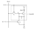
- 빛을 발생시키는 유기 발광 소자;전원 전압이 인가되는 제 1 전극, 상기 유기 발광 소자에 전기적으로 연결되는 제2 전극, 및 게이트 전극을 구비하는 제 1 트랜지스터;데이터 신호가 인가되는 제 1 전극, 상기 제 1 트랜지스터의 상기 게이트 전극에 연결되는 제 2 전극, 및 제 1 주사 신호가 인가되는 게이트 전극을 구비하는 제 2 트랜지스터;상기 제 1 트랜지스터의 상기 게이트 전극에 연결되는 제 1 단자, 및 상기 제1 트랜지스터의 상기 제 1 전극에 연결되는 제 2 단자를 구비하는 커패시터; 및상기 제 1 트랜지스터의 게이트 전극에 연결되는 제 1 전극, 접지 전압이 인가되는 제 2 전극, 및 제 2 주사 신호가 인가되는 게이트 전극을 구비하는 제 3 트랜지스터를 포함하며,상기 제 2 주사 신호는 상기 제 1 주사 신호가 인가되기 직전에 인접 화소에 인가되는 주사 신호인 것을 특징으로 하는 유기 발광 표시장치.
- 제1항에 있어서,상기 유기 발광 표시 장치는 화소 회로를 포함하는 화소 영역; 및상기 화소 영역의 외부에 구비되며, 상기 화소 회로를 구동하는 구동회로를 구비하는 비화소 영역을 포함하는 것을 특징으로 하는 유기 발광 표시장치.
- 제2항에 있어서, 상기 제 3 트랜지스터는 상기 화소 영역에 포함되는 것을 특징으로 하는 유기 발광 표시장치.
- 제3항에 있어서,상기 유기 발광 표시장치는 전면발광 구조인 것을 특징으로 하는 유기 발광 표시장치.
- 제2항에 있어서, 상기 제 3 트랜지스터는 상기 비화소 영역에 포함되는 것을 특징으로 하는 유기 발광 표시장치.
- 제5항에 있어서, 상기 비화소 영역에상기 제 1 주사 신호 및 제 2 주사 신호를 전달하는 복수의 주사선들과 상기 복수의 주사선들에 제 1 주사 신호 및 제 2 주사 신호를 공급하는 주사 구동부;상기 데이터 신호를 전달하는 복수의 데이터선들과 상기 복수의 데이터선들에 데이터 신호를 공급하는 데이터 구동부을 포함하는 것을 특징으로 하는 유기 발광 표시장치.
- 제6항에 있어서, 상기 제 3 트랜지스터는상기 주사 구동부와 상기 화소 영역 사이 구비되는 것을 특징으로 하는 유기 발광 표시장치.
- 제1항에 있어서,상기 제 1 내지 제 3 트랜지스터는 NMOS 트랜지스터인 것을 특징으로 하는 유기 발광 표시장치.
- 제8항에 있어서,상기 제 1 내지 제 3 트랜지스터는 산화물 TFT인 것을 특징으로 하는 유기 발광 표시장치.
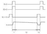
- a) 제 1 주사 신호 및 데이터 신호를 인가받아 상기 데이터 신호에 해당하는 전압을 커패시터에 충전하는 단계;b) 상기 충전한 전압을 사용하여 유기 발광 소자를 발광시키는 단계; 및c) 제 2 주사 신호에 따라서 상기 커패시터에 잔류하는 전하를 방전시키는 단계를 포함하는 유기 발광 표시장치의 구동방법.
- 제10항에 있어서,상기 제 2 주사 신호는 상기 제 1 주사 신호가 인가되기 직전에 인접 화소에 인가되는 주사 신호인 것을 특징으로 하는 유기 발광 표시장치의 구동방법.
- 제10항에 있어서, 상기 c)단계는상기 제 2 주사 신호에 따라서 커패시터를 접지시키는 것을 특징으로 하는 유기 발광 표시장치의 구동방법.
Priority Applications (2)
| Application Number | Priority Date | Filing Date | Title |
|---|---|---|---|
| KR1020080031705A KR20090106162A (ko) | 2008-04-04 | 2008-04-04 | 유기 발광 표시장치 및 그 구동방법 |
| US12/385,307 US8384701B2 (en) | 2008-04-04 | 2009-04-03 | Organic light emitting display apparatus and method of driving the same |
Applications Claiming Priority (1)
| Application Number | Priority Date | Filing Date | Title |
|---|---|---|---|
| KR1020080031705A KR20090106162A (ko) | 2008-04-04 | 2008-04-04 | 유기 발광 표시장치 및 그 구동방법 |
Related Child Applications (1)
| Application Number | Title | Priority Date | Filing Date |
|---|---|---|---|
| KR1020100019576A Division KR20100029811A (ko) | 2010-03-04 | 2010-03-04 | 유기 발광 표시장치 및 그 구동방법 |
Publications (1)
| Publication Number | Publication Date |
|---|---|
| KR20090106162A true KR20090106162A (ko) | 2009-10-08 |
Family
ID=41132831
Family Applications (1)
| Application Number | Title | Priority Date | Filing Date |
|---|---|---|---|
| KR1020080031705A Ceased KR20090106162A (ko) | 2008-04-04 | 2008-04-04 | 유기 발광 표시장치 및 그 구동방법 |
Country Status (2)
| Country | Link |
|---|---|
| US (1) | US8384701B2 (ko) |
| KR (1) | KR20090106162A (ko) |
Cited By (4)
| Publication number | Priority date | Publication date | Assignee | Title |
|---|---|---|---|---|
| US8686926B2 (en) | 2010-06-30 | 2014-04-01 | Samsung Display Co., Ltd. | Organic light emitting display device and pixel circuit |
| US8803770B2 (en) | 2010-06-30 | 2014-08-12 | Samsung Display Co., Ltd. | Pixel and an organic light emitting display device using the same |
| CN107863056A (zh) * | 2016-09-21 | 2018-03-30 | 三星显示有限公司 | 显示装置及其制造方法 |
| KR20230145003A (ko) * | 2011-05-25 | 2023-10-17 | 가부시키가이샤 한도오따이 에네루기 켄큐쇼 | 산화물 반도체막의 성막 방법, 반도체 장치 및 반도체 장치의 제작 방법 |
Families Citing this family (12)
| Publication number | Priority date | Publication date | Assignee | Title |
|---|---|---|---|---|
| KR20090106162A (ko) * | 2008-04-04 | 2009-10-08 | 삼성모바일디스플레이주식회사 | 유기 발광 표시장치 및 그 구동방법 |
| KR101692367B1 (ko) * | 2010-07-22 | 2017-01-04 | 삼성디스플레이 주식회사 | 화소 및 이를 이용한 유기전계발광 표시장치 |
| KR101822498B1 (ko) * | 2010-12-10 | 2018-01-29 | 삼성디스플레이 주식회사 | 표시 장치를 위한 화소, 이를 이용하는 표시 장치 및 그 구동 방법 |
| US9886899B2 (en) * | 2011-05-17 | 2018-02-06 | Ignis Innovation Inc. | Pixel Circuits for AMOLED displays |
| KR102023183B1 (ko) * | 2012-11-20 | 2019-09-20 | 삼성디스플레이 주식회사 | 화소, 이를 포함하는 표시장치 및 그 구동 방법 |
| CA2894717A1 (en) | 2015-06-19 | 2016-12-19 | Ignis Innovation Inc. | Optoelectronic device characterization in array with shared sense line |
| TW201508908A (zh) | 2013-08-19 | 2015-03-01 | Chunghwa Picture Tubes Ltd | 有機發光二極體的畫素電路 |
| KR102527226B1 (ko) * | 2015-11-23 | 2023-05-02 | 삼성디스플레이 주식회사 | 유기 발광 표시 장치 |
| CN106803417A (zh) | 2017-03-02 | 2017-06-06 | 深圳市华星光电技术有限公司 | 像素补偿电路及驱动方法、显示装置 |
| KR20220007826A (ko) * | 2020-07-10 | 2022-01-19 | 삼성디스플레이 주식회사 | 디스플레이 장치 및 그 제조방법 |
| CN113035139A (zh) * | 2021-03-19 | 2021-06-25 | Tcl华星光电技术有限公司 | 一种背光驱动电路及液晶显示装置 |
| EP4300474A4 (en) | 2021-07-30 | 2024-02-28 | BOE Technology Group Co., Ltd. | PIXEL CIRCUIT, CONTROL METHOD AND DISPLAY DEVICE |
Family Cites Families (13)
| Publication number | Priority date | Publication date | Assignee | Title |
|---|---|---|---|---|
| JP2002351401A (ja) * | 2001-03-21 | 2002-12-06 | Mitsubishi Electric Corp | 自発光型表示装置 |
| KR100469344B1 (ko) | 2001-10-30 | 2005-02-02 | 엘지.필립스 엘시디 주식회사 | 전계발광 디스플레이 패널 및 그의 구동방법 |
| US20030103022A1 (en) * | 2001-11-09 | 2003-06-05 | Yukihiro Noguchi | Display apparatus with function for initializing luminance data of optical element |
| TW589596B (en) * | 2002-07-19 | 2004-06-01 | Au Optronics Corp | Driving circuit of display able to prevent the accumulated charges |
| JP2004246320A (ja) * | 2003-01-20 | 2004-09-02 | Sanyo Electric Co Ltd | アクティブマトリクス駆動型表示装置 |
| JP4016962B2 (ja) * | 2003-05-19 | 2007-12-05 | セイコーエプソン株式会社 | 電気光学装置、電気光学装置の駆動方法 |
| KR100560780B1 (ko) * | 2003-07-07 | 2006-03-13 | 삼성에스디아이 주식회사 | 유기전계 발광표시장치의 화소회로 및 그의 구동방법 |
| US7053875B2 (en) * | 2004-08-21 | 2006-05-30 | Chen-Jean Chou | Light emitting device display circuit and drive method thereof |
| KR100653846B1 (ko) * | 2005-04-11 | 2006-12-05 | 실리콘 디스플레이 (주) | 유기 발광 다이오드의 구동 회로 및 구동 방법 |
| KR100747261B1 (ko) | 2005-09-05 | 2007-08-07 | 엘지전자 주식회사 | 유기전계발광소자 및 그 표시장치, 그 구동방법 |
| TWI276029B (en) * | 2005-11-28 | 2007-03-11 | Chi Mei El Corp | Organic light-emitting display and voltage-driven organic light-emitting pixel |
| KR20070111638A (ko) * | 2006-05-18 | 2007-11-22 | 엘지.필립스 엘시디 주식회사 | 유기전계발광표시장치의 화소 회로 |
| KR20090106162A (ko) * | 2008-04-04 | 2009-10-08 | 삼성모바일디스플레이주식회사 | 유기 발광 표시장치 및 그 구동방법 |
-
2008
- 2008-04-04 KR KR1020080031705A patent/KR20090106162A/ko not_active Ceased
-
2009
- 2009-04-03 US US12/385,307 patent/US8384701B2/en active Active
Cited By (5)
| Publication number | Priority date | Publication date | Assignee | Title |
|---|---|---|---|---|
| US8686926B2 (en) | 2010-06-30 | 2014-04-01 | Samsung Display Co., Ltd. | Organic light emitting display device and pixel circuit |
| US8803770B2 (en) | 2010-06-30 | 2014-08-12 | Samsung Display Co., Ltd. | Pixel and an organic light emitting display device using the same |
| KR20230145003A (ko) * | 2011-05-25 | 2023-10-17 | 가부시키가이샤 한도오따이 에네루기 켄큐쇼 | 산화물 반도체막의 성막 방법, 반도체 장치 및 반도체 장치의 제작 방법 |
| US12170339B2 (en) | 2011-05-25 | 2024-12-17 | Semiconductor Energy Laboratory Co., Ltd. | Method for forming oxide semiconductor film, semiconductor device, and method for manufacturing semiconductor device |
| CN107863056A (zh) * | 2016-09-21 | 2018-03-30 | 三星显示有限公司 | 显示装置及其制造方法 |
Also Published As
| Publication number | Publication date |
|---|---|
| US8384701B2 (en) | 2013-02-26 |
| US20090251452A1 (en) | 2009-10-08 |
Similar Documents
| Publication | Publication Date | Title |
|---|---|---|
| KR20090106162A (ko) | 유기 발광 표시장치 및 그 구동방법 | |
| KR100536235B1 (ko) | 화상 표시 장치 및 그 구동 방법 | |
| JP4396848B2 (ja) | 発光表示装置 | |
| JP4728849B2 (ja) | 表示装置及びその駆動方法 | |
| KR100926591B1 (ko) | 유기 전계 발광 표시 장치 | |
| US7277071B2 (en) | Luminescent display, and driving method and pixel circuit thereof, and display device | |
| KR100612392B1 (ko) | 발광 표시 장치 및 발광 표시 패널 | |
| CN100380423C (zh) | 有机电致发光显示器及其驱动方法 | |
| US7403176B2 (en) | Image display device, and display panel and driving method thereof, and pixel circuit | |
| US6864637B2 (en) | Organic electro luminescence device and method for driving the same | |
| JP5080733B2 (ja) | 表示装置及びその駆動方法 | |
| KR100515351B1 (ko) | 표시 패널, 이를 이용한 발광 표시 장치 및 그 구동 방법 | |
| KR101368006B1 (ko) | 유기전계발광표시장치 및 이의 구동방법 | |
| US20070152923A1 (en) | Light emitting display and method of driving thereof | |
| KR100536237B1 (ko) | 발광 표시 장치 및 그 구동 방법 | |
| KR101493223B1 (ko) | 유기발광 표시장치 | |
| KR100899158B1 (ko) | 액티브 매트릭스형 유기 전계발광 표시패널 및 그의제조방법 | |
| KR20100029811A (ko) | 유기 발광 표시장치 및 그 구동방법 | |
| KR100538331B1 (ko) | 일렉트로 루미네센스 표시장치 | |
| KR101240658B1 (ko) | 표시 장치 및 그 구동 방법 |
Legal Events
| Date | Code | Title | Description |
|---|---|---|---|
| A201 | Request for examination | ||
| PA0109 | Patent application |
Patent event code: PA01091R01D Comment text: Patent Application Patent event date: 20080404 |
|
| PA0201 | Request for examination | ||
| N231 | Notification of change of applicant | ||
| PN2301 | Change of applicant |
Patent event date: 20081120 Comment text: Notification of Change of Applicant Patent event code: PN23011R01D |
|
| E902 | Notification of reason for refusal | ||
| PE0902 | Notice of grounds for rejection |
Comment text: Notification of reason for refusal Patent event date: 20090623 Patent event code: PE09021S01D |
|
| AMND | Amendment | ||
| E90F | Notification of reason for final refusal | ||
| PE0902 | Notice of grounds for rejection |
Comment text: Final Notice of Reason for Refusal Patent event date: 20090828 Patent event code: PE09021S02D |
|
| PG1501 | Laying open of application | ||
| AMND | Amendment | ||
| E601 | Decision to refuse application | ||
| E801 | Decision on dismissal of amendment | ||
| PE0601 | Decision on rejection of patent |
Patent event date: 20091030 Comment text: Decision to Refuse Application Patent event code: PE06012S01D Patent event date: 20090828 Comment text: Final Notice of Reason for Refusal Patent event code: PE06011S02I Patent event date: 20090623 Comment text: Notification of reason for refusal Patent event code: PE06011S01I |
|
| PE0801 | Dismissal of amendment |
Patent event code: PE08012E01D Comment text: Decision on Dismissal of Amendment Patent event date: 20091030 Patent event code: PE08011R01I Comment text: Amendment to Specification, etc. Patent event date: 20091028 Patent event code: PE08011R01I Comment text: Amendment to Specification, etc. Patent event date: 20090824 |
|
| AMND | Amendment | ||
| J201 | Request for trial against refusal decision | ||
| PJ0201 | Trial against decision of rejection |
Patent event date: 20091130 Comment text: Request for Trial against Decision on Refusal Patent event code: PJ02012R01D Patent event date: 20091030 Comment text: Decision to Refuse Application Patent event code: PJ02011S01I Appeal kind category: Appeal against decision to decline refusal Decision date: 20110722 Appeal identifier: 2009101010887 Request date: 20091130 |
|
| PB0901 | Examination by re-examination before a trial |
Comment text: Amendment to Specification, etc. Patent event date: 20091130 Patent event code: PB09011R02I Comment text: Request for Trial against Decision on Refusal Patent event date: 20091130 Patent event code: PB09011R01I Comment text: Amendment to Specification, etc. Patent event date: 20091028 Patent event code: PB09011R02I Comment text: Amendment to Specification, etc. Patent event date: 20090824 Patent event code: PB09011R02I |
|
| E902 | Notification of reason for refusal | ||
| PE0902 | Notice of grounds for rejection |
Comment text: Notification of reason for refusal Patent event date: 20100107 Patent event code: PE09021S01D |
|
| A107 | Divisional application of patent | ||
| PA0107 | Divisional application |
Comment text: Divisional Application of Patent Patent event date: 20100304 Patent event code: PA01071R01D |
|
| B601 | Maintenance of original decision after re-examination before a trial | ||
| PB0601 | Maintenance of original decision after re-examination before a trial |
Comment text: Report of Result of Re-examination before a Trial Patent event code: PB06011S01D Patent event date: 20100317 |
|
| J301 | Trial decision |
Free format text: TRIAL NUMBER: 2009101010887; TRIAL DECISION FOR APPEAL AGAINST DECISION TO DECLINE REFUSAL REQUESTED 20091130 Effective date: 20110722 Free format text: TRIAL DECISION FOR APPEAL AGAINST DECISION TO DECLINE REFUSAL REQUESTED 20091130 Effective date: 20110722 |
|
| PJ1301 | Trial decision |
Patent event code: PJ13011S01D Patent event date: 20110722 Comment text: Trial Decision on Objection to Decision on Refusal Appeal kind category: Appeal against decision to decline refusal Request date: 20091130 Decision date: 20110722 Appeal identifier: 2009101010887 |