KR20110000726A - 웨이퍼에 칩을 본딩하는 방법 - Google Patents
웨이퍼에 칩을 본딩하는 방법 Download PDFInfo
- Publication number
- KR20110000726A KR20110000726A KR1020107017670A KR20107017670A KR20110000726A KR 20110000726 A KR20110000726 A KR 20110000726A KR 1020107017670 A KR1020107017670 A KR 1020107017670A KR 20107017670 A KR20107017670 A KR 20107017670A KR 20110000726 A KR20110000726 A KR 20110000726A
- Authority
- KR
- South Korea
- Prior art keywords
- support wafer
- chips
- chip
- wafer
- bonding
- Prior art date
- Legal status (The legal status is an assumption and is not a legal conclusion. Google has not performed a legal analysis and makes no representation as to the accuracy of the status listed.)
- Ceased
Links
Images


Classifications
-
- B—PERFORMING OPERATIONS; TRANSPORTING
- B62—LAND VEHICLES FOR TRAVELLING OTHERWISE THAN ON RAILS
- B62H—CYCLE STANDS; SUPPORTS OR HOLDERS FOR PARKING OR STORING CYCLES; APPLIANCES PREVENTING OR INDICATING UNAUTHORIZED USE OR THEFT OF CYCLES; LOCKS INTEGRAL WITH CYCLES; DEVICES FOR LEARNING TO RIDE CYCLES
- B62H3/00—Separate supports or holders for parking or storing cycles
- B62H3/04—Separate supports or holders for parking or storing cycles involving forked supports of brackets for holding a wheel
-
- H—ELECTRICITY
- H10—SEMICONDUCTOR DEVICES; ELECTRIC SOLID-STATE DEVICES NOT OTHERWISE PROVIDED FOR
- H10P—GENERIC PROCESSES OR APPARATUS FOR THE MANUFACTURE OR TREATMENT OF DEVICES COVERED BY CLASS H10
- H10P72/00—Handling or holding of wafers, substrates or devices during manufacture or treatment thereof
- H10P72/70—Handling or holding of wafers, substrates or devices during manufacture or treatment thereof for supporting or gripping
- H10P72/74—Handling or holding of wafers, substrates or devices during manufacture or treatment thereof for supporting or gripping using temporarily an auxiliary support
-
- H—ELECTRICITY
- H10—SEMICONDUCTOR DEVICES; ELECTRIC SOLID-STATE DEVICES NOT OTHERWISE PROVIDED FOR
- H10P—GENERIC PROCESSES OR APPARATUS FOR THE MANUFACTURE OR TREATMENT OF DEVICES COVERED BY CLASS H10
- H10P72/00—Handling or holding of wafers, substrates or devices during manufacture or treatment thereof
- H10P72/70—Handling or holding of wafers, substrates or devices during manufacture or treatment thereof for supporting or gripping
- H10P72/74—Handling or holding of wafers, substrates or devices during manufacture or treatment thereof for supporting or gripping using temporarily an auxiliary support
- H10P72/7402—Wafer tapes, e.g. grinding or dicing support tapes
-
- H—ELECTRICITY
- H10—SEMICONDUCTOR DEVICES; ELECTRIC SOLID-STATE DEVICES NOT OTHERWISE PROVIDED FOR
- H10W—GENERIC PACKAGES, INTERCONNECTIONS, CONNECTORS OR OTHER CONSTRUCTIONAL DETAILS OF DEVICES COVERED BY CLASS H10
- H10W90/00—Package configurations
-
- H—ELECTRICITY
- H10—SEMICONDUCTOR DEVICES; ELECTRIC SOLID-STATE DEVICES NOT OTHERWISE PROVIDED FOR
- H10P—GENERIC PROCESSES OR APPARATUS FOR THE MANUFACTURE OR TREATMENT OF DEVICES COVERED BY CLASS H10
- H10P72/00—Handling or holding of wafers, substrates or devices during manufacture or treatment thereof
- H10P72/70—Handling or holding of wafers, substrates or devices during manufacture or treatment thereof for supporting or gripping
- H10P72/74—Handling or holding of wafers, substrates or devices during manufacture or treatment thereof for supporting or gripping using temporarily an auxiliary support
- H10P72/7416—Handling or holding of wafers, substrates or devices during manufacture or treatment thereof for supporting or gripping using temporarily an auxiliary support used during dicing or grinding
- H10P72/7418—Handling or holding of wafers, substrates or devices during manufacture or treatment thereof for supporting or gripping using temporarily an auxiliary support used during dicing or grinding of passive members, e.g. a chip mounting substrate
-
- H—ELECTRICITY
- H10—SEMICONDUCTOR DEVICES; ELECTRIC SOLID-STATE DEVICES NOT OTHERWISE PROVIDED FOR
- H10W—GENERIC PACKAGES, INTERCONNECTIONS, CONNECTORS OR OTHER CONSTRUCTIONAL DETAILS OF DEVICES COVERED BY CLASS H10
- H10W72/00—Interconnections or connectors in packages
- H10W72/01—Manufacture or treatment
- H10W72/016—Manufacture or treatment of strap connectors
-
- H—ELECTRICITY
- H10—SEMICONDUCTOR DEVICES; ELECTRIC SOLID-STATE DEVICES NOT OTHERWISE PROVIDED FOR
- H10W—GENERIC PACKAGES, INTERCONNECTIONS, CONNECTORS OR OTHER CONSTRUCTIONAL DETAILS OF DEVICES COVERED BY CLASS H10
- H10W72/00—Interconnections or connectors in packages
- H10W72/01—Manufacture or treatment
- H10W72/0198—Manufacture or treatment batch processes
-
- H—ELECTRICITY
- H10—SEMICONDUCTOR DEVICES; ELECTRIC SOLID-STATE DEVICES NOT OTHERWISE PROVIDED FOR
- H10W—GENERIC PACKAGES, INTERCONNECTIONS, CONNECTORS OR OTHER CONSTRUCTIONAL DETAILS OF DEVICES COVERED BY CLASS H10
- H10W72/00—Interconnections or connectors in packages
- H10W72/071—Connecting or disconnecting
- H10W72/072—Connecting or disconnecting of bump connectors
-
- H—ELECTRICITY
- H10—SEMICONDUCTOR DEVICES; ELECTRIC SOLID-STATE DEVICES NOT OTHERWISE PROVIDED FOR
- H10W—GENERIC PACKAGES, INTERCONNECTIONS, CONNECTORS OR OTHER CONSTRUCTIONAL DETAILS OF DEVICES COVERED BY CLASS H10
- H10W72/00—Interconnections or connectors in packages
- H10W72/071—Connecting or disconnecting
- H10W72/072—Connecting or disconnecting of bump connectors
- H10W72/07202—Connecting or disconnecting of bump connectors using auxiliary members
- H10W72/07204—Connecting or disconnecting of bump connectors using auxiliary members using temporary auxiliary members, e.g. sacrificial coatings
- H10W72/07207—Temporary substrates, e.g. removable substrates
-
- H—ELECTRICITY
- H10—SEMICONDUCTOR DEVICES; ELECTRIC SOLID-STATE DEVICES NOT OTHERWISE PROVIDED FOR
- H10W—GENERIC PACKAGES, INTERCONNECTIONS, CONNECTORS OR OTHER CONSTRUCTIONAL DETAILS OF DEVICES COVERED BY CLASS H10
- H10W72/00—Interconnections or connectors in packages
- H10W72/071—Connecting or disconnecting
- H10W72/072—Connecting or disconnecting of bump connectors
- H10W72/07231—Techniques
- H10W72/07236—Soldering or alloying
-
- H—ELECTRICITY
- H10—SEMICONDUCTOR DEVICES; ELECTRIC SOLID-STATE DEVICES NOT OTHERWISE PROVIDED FOR
- H10W—GENERIC PACKAGES, INTERCONNECTIONS, CONNECTORS OR OTHER CONSTRUCTIONAL DETAILS OF DEVICES COVERED BY CLASS H10
- H10W72/00—Interconnections or connectors in packages
- H10W72/071—Connecting or disconnecting
- H10W72/072—Connecting or disconnecting of bump connectors
- H10W72/07251—Connecting or disconnecting of bump connectors characterised by changes in properties of the bump connectors during connecting
- H10W72/07254—Connecting or disconnecting of bump connectors characterised by changes in properties of the bump connectors during connecting changes in dispositions
-
- H—ELECTRICITY
- H10—SEMICONDUCTOR DEVICES; ELECTRIC SOLID-STATE DEVICES NOT OTHERWISE PROVIDED FOR
- H10W—GENERIC PACKAGES, INTERCONNECTIONS, CONNECTORS OR OTHER CONSTRUCTIONAL DETAILS OF DEVICES COVERED BY CLASS H10
- H10W72/00—Interconnections or connectors in packages
- H10W72/071—Connecting or disconnecting
- H10W72/075—Connecting or disconnecting of bond wires
-
- H—ELECTRICITY
- H10—SEMICONDUCTOR DEVICES; ELECTRIC SOLID-STATE DEVICES NOT OTHERWISE PROVIDED FOR
- H10W—GENERIC PACKAGES, INTERCONNECTIONS, CONNECTORS OR OTHER CONSTRUCTIONAL DETAILS OF DEVICES COVERED BY CLASS H10
- H10W72/00—Interconnections or connectors in packages
- H10W72/20—Bump connectors, e.g. solder bumps or copper pillars; Dummy bumps; Thermal bumps
- H10W72/221—Structures or relative sizes
-
- H—ELECTRICITY
- H10—SEMICONDUCTOR DEVICES; ELECTRIC SOLID-STATE DEVICES NOT OTHERWISE PROVIDED FOR
- H10W—GENERIC PACKAGES, INTERCONNECTIONS, CONNECTORS OR OTHER CONSTRUCTIONAL DETAILS OF DEVICES COVERED BY CLASS H10
- H10W72/00—Interconnections or connectors in packages
- H10W72/20—Bump connectors, e.g. solder bumps or copper pillars; Dummy bumps; Thermal bumps
- H10W72/221—Structures or relative sizes
- H10W72/227—Multiple bumps having different sizes
-
- H—ELECTRICITY
- H10—SEMICONDUCTOR DEVICES; ELECTRIC SOLID-STATE DEVICES NOT OTHERWISE PROVIDED FOR
- H10W—GENERIC PACKAGES, INTERCONNECTIONS, CONNECTORS OR OTHER CONSTRUCTIONAL DETAILS OF DEVICES COVERED BY CLASS H10
- H10W72/00—Interconnections or connectors in packages
- H10W72/20—Bump connectors, e.g. solder bumps or copper pillars; Dummy bumps; Thermal bumps
- H10W72/241—Dispositions, e.g. layouts
- H10W72/244—Dispositions, e.g. layouts relative to underlying supporting features, e.g. bond pads, RDLs or vias
-
- H—ELECTRICITY
- H10—SEMICONDUCTOR DEVICES; ELECTRIC SOLID-STATE DEVICES NOT OTHERWISE PROVIDED FOR
- H10W—GENERIC PACKAGES, INTERCONNECTIONS, CONNECTORS OR OTHER CONSTRUCTIONAL DETAILS OF DEVICES COVERED BY CLASS H10
- H10W72/00—Interconnections or connectors in packages
- H10W72/20—Bump connectors, e.g. solder bumps or copper pillars; Dummy bumps; Thermal bumps
- H10W72/241—Dispositions, e.g. layouts
- H10W72/247—Dispositions of multiple bumps
-
- H—ELECTRICITY
- H10—SEMICONDUCTOR DEVICES; ELECTRIC SOLID-STATE DEVICES NOT OTHERWISE PROVIDED FOR
- H10W—GENERIC PACKAGES, INTERCONNECTIONS, CONNECTORS OR OTHER CONSTRUCTIONAL DETAILS OF DEVICES COVERED BY CLASS H10
- H10W72/00—Interconnections or connectors in packages
- H10W72/20—Bump connectors, e.g. solder bumps or copper pillars; Dummy bumps; Thermal bumps
- H10W72/241—Dispositions, e.g. layouts
- H10W72/247—Dispositions of multiple bumps
- H10W72/248—Top-view layouts, e.g. mirror arrays
-
- H—ELECTRICITY
- H10—SEMICONDUCTOR DEVICES; ELECTRIC SOLID-STATE DEVICES NOT OTHERWISE PROVIDED FOR
- H10W—GENERIC PACKAGES, INTERCONNECTIONS, CONNECTORS OR OTHER CONSTRUCTIONAL DETAILS OF DEVICES COVERED BY CLASS H10
- H10W72/00—Interconnections or connectors in packages
- H10W72/20—Bump connectors, e.g. solder bumps or copper pillars; Dummy bumps; Thermal bumps
- H10W72/29—Bond pads specially adapted therefor
-
- H—ELECTRICITY
- H10—SEMICONDUCTOR DEVICES; ELECTRIC SOLID-STATE DEVICES NOT OTHERWISE PROVIDED FOR
- H10W—GENERIC PACKAGES, INTERCONNECTIONS, CONNECTORS OR OTHER CONSTRUCTIONAL DETAILS OF DEVICES COVERED BY CLASS H10
- H10W72/00—Interconnections or connectors in packages
- H10W72/50—Bond wires
- H10W72/59—Bond pads specially adapted therefor
-
- H—ELECTRICITY
- H10—SEMICONDUCTOR DEVICES; ELECTRIC SOLID-STATE DEVICES NOT OTHERWISE PROVIDED FOR
- H10W—GENERIC PACKAGES, INTERCONNECTIONS, CONNECTORS OR OTHER CONSTRUCTIONAL DETAILS OF DEVICES COVERED BY CLASS H10
- H10W72/00—Interconnections or connectors in packages
- H10W72/851—Dispositions of multiple connectors or interconnections
- H10W72/853—On the same surface
- H10W72/859—Bump connectors and bond wires
-
- H—ELECTRICITY
- H10—SEMICONDUCTOR DEVICES; ELECTRIC SOLID-STATE DEVICES NOT OTHERWISE PROVIDED FOR
- H10W—GENERIC PACKAGES, INTERCONNECTIONS, CONNECTORS OR OTHER CONSTRUCTIONAL DETAILS OF DEVICES COVERED BY CLASS H10
- H10W72/00—Interconnections or connectors in packages
- H10W72/90—Bond pads, in general
- H10W72/941—Dispositions of bond pads
- H10W72/942—Dispositions of bond pads relative to underlying supporting features, e.g. bond pads, RDLs or vias
-
- H—ELECTRICITY
- H10—SEMICONDUCTOR DEVICES; ELECTRIC SOLID-STATE DEVICES NOT OTHERWISE PROVIDED FOR
- H10W—GENERIC PACKAGES, INTERCONNECTIONS, CONNECTORS OR OTHER CONSTRUCTIONAL DETAILS OF DEVICES COVERED BY CLASS H10
- H10W74/00—Encapsulations, e.g. protective coatings
- H10W74/10—Encapsulations, e.g. protective coatings characterised by their shape or disposition
- H10W74/111—Encapsulations, e.g. protective coatings characterised by their shape or disposition the semiconductor body being completely enclosed
- H10W74/114—Encapsulations, e.g. protective coatings characterised by their shape or disposition the semiconductor body being completely enclosed by a substrate and the encapsulations
- H10W74/117—Encapsulations, e.g. protective coatings characterised by their shape or disposition the semiconductor body being completely enclosed by a substrate and the encapsulations the substrate having spherical bumps for external connection
-
- H—ELECTRICITY
- H10—SEMICONDUCTOR DEVICES; ELECTRIC SOLID-STATE DEVICES NOT OTHERWISE PROVIDED FOR
- H10W—GENERIC PACKAGES, INTERCONNECTIONS, CONNECTORS OR OTHER CONSTRUCTIONAL DETAILS OF DEVICES COVERED BY CLASS H10
- H10W90/00—Package configurations
- H10W90/20—Configurations of stacked chips
- H10W90/297—Configurations of stacked chips characterised by the through-semiconductor vias [TSVs] in the stacked chips
-
- H—ELECTRICITY
- H10—SEMICONDUCTOR DEVICES; ELECTRIC SOLID-STATE DEVICES NOT OTHERWISE PROVIDED FOR
- H10W—GENERIC PACKAGES, INTERCONNECTIONS, CONNECTORS OR OTHER CONSTRUCTIONAL DETAILS OF DEVICES COVERED BY CLASS H10
- H10W90/00—Package configurations
- H10W90/701—Package configurations characterised by the relative positions of pads or connectors relative to package parts
- H10W90/721—Package configurations characterised by the relative positions of pads or connectors relative to package parts of bump connectors
- H10W90/722—Package configurations characterised by the relative positions of pads or connectors relative to package parts of bump connectors between stacked chips
-
- H—ELECTRICITY
- H10—SEMICONDUCTOR DEVICES; ELECTRIC SOLID-STATE DEVICES NOT OTHERWISE PROVIDED FOR
- H10W—GENERIC PACKAGES, INTERCONNECTIONS, CONNECTORS OR OTHER CONSTRUCTIONAL DETAILS OF DEVICES COVERED BY CLASS H10
- H10W90/00—Package configurations
- H10W90/701—Package configurations characterised by the relative positions of pads or connectors relative to package parts
- H10W90/721—Package configurations characterised by the relative positions of pads or connectors relative to package parts of bump connectors
- H10W90/724—Package configurations characterised by the relative positions of pads or connectors relative to package parts of bump connectors between a chip and a stacked insulating package substrate, interposer or RDL
-
- H—ELECTRICITY
- H10—SEMICONDUCTOR DEVICES; ELECTRIC SOLID-STATE DEVICES NOT OTHERWISE PROVIDED FOR
- H10W—GENERIC PACKAGES, INTERCONNECTIONS, CONNECTORS OR OTHER CONSTRUCTIONAL DETAILS OF DEVICES COVERED BY CLASS H10
- H10W90/00—Package configurations
- H10W90/701—Package configurations characterised by the relative positions of pads or connectors relative to package parts
- H10W90/751—Package configurations characterised by the relative positions of pads or connectors relative to package parts of bond wires
- H10W90/754—Package configurations characterised by the relative positions of pads or connectors relative to package parts of bond wires between a chip and a stacked insulating package substrate, interposer or RDL
-
- H—ELECTRICITY
- H10—SEMICONDUCTOR DEVICES; ELECTRIC SOLID-STATE DEVICES NOT OTHERWISE PROVIDED FOR
- H10W—GENERIC PACKAGES, INTERCONNECTIONS, CONNECTORS OR OTHER CONSTRUCTIONAL DETAILS OF DEVICES COVERED BY CLASS H10
- H10W90/00—Package configurations
- H10W90/701—Package configurations characterised by the relative positions of pads or connectors relative to package parts
- H10W90/751—Package configurations characterised by the relative positions of pads or connectors relative to package parts of bond wires
- H10W90/756—Package configurations characterised by the relative positions of pads or connectors relative to package parts of bond wires between a chip and a stacked lead frame, conducting package substrate or heat sink
Landscapes
- Engineering & Computer Science (AREA)
- Mechanical Engineering (AREA)
- Wire Bonding (AREA)
- Manufacturing & Machinery (AREA)
Abstract
Description
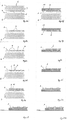
도 2a 내지 2m은 본 발명의 첫 번째 실시예에 따르는 방법 시퀀스를 개략적으로 나타낸다.
도 3a는 본 발명에 따르는 칩 스택을 개략적으로 도시한다.
도 3b는 복수의 칩을 갖는 본 발명에 따르는 칩 스택을 개략적으로 도시한다.
도 4a 내지 4i는 본 발명의 두 번째 실시예에 따르는 방법 시퀀스를 개략적으로 도시한다.
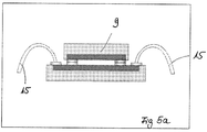
도 5a는 본 발명에 따라 생산된 칩을 개략적으로 도시한다.
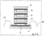
도 5b는 복수의 칩을 포함하는 본 발명에 따라 생산된 칩 스택을 개략적으로 도시한다.
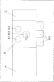
B : 핸들링 모듈
B.1 : 이송 스테이션
B.2 : 테이프 제거 스테이션
B.3 : 로봇 암을 갖는 로봇
B.4 : 카세트 스테이션
C : 본딩 스테이션
1 : 지지 웨이퍼
2 : 앞면
3 : 칩
4 : 연결 수단
5 : 캐리어
6 : 뒷면
7 : 전기 전도성 연결
8 : 전기 전도성 박막
9 : 개별 칩
10 : 칩 측면
11 : 매스
12 : 솔더 범프
13 : 다이싱 프레임
14 : 뒷면-그라인딩 테이프
15 : 라인 세트
Claims (20)
- 복수의 칩(3)을 지지 웨이퍼(1)에 본딩하기 위한 방법에 있어서, 이때 상기 칩(3)은 지지 웨이퍼(1) 위에서 복수 층으로 적층되며, 수직으로 이웃하는 칩들(3) 사이에, 그리고 지지 웨이퍼(1)와 상기 지지 웨이퍼(1)와 수직으로 이웃하고 있는 칩(3)의 층 사이에 전기 전도성 연결(7)이 존재하고, 상기 방법은
a) 지지 웨이퍼(1)를 캐리어(5) 상에 고정하는 단계와,
b) 칩(3)의 하나 이상의 층을 상기 지지 웨이퍼(1) 상의 지정 위치로 배치하는 단계와,
c) 캐리어(5)에 고정되어 있는 지지 웨이퍼(1) 상의 칩(3)을 열처리하는 단계
를 포함하는 것을 특징으로 하는 복수의 칩을 하나의 지지 웨이퍼로 본딩하기 위한 방법. - 제 1 항에 있어서, 상기 단계 b) 및 c)는 서로 다른 장치에서 수행되는 것을 특징으로 하는 복수의 칩을 지지 웨이퍼에 본딩하기 위한 방법.
- 제 1 항 또는 제 2 항에 있어서, 상기 캐리어(5)는, 부분적으로, 또는 전적으로 실리콘으로 구성되며, 상기 캐리어(5)의 크기는 지지 웨이퍼(1)의 크기와 일치하거나, 캐리어 반경이 지지 웨이퍼 반경에서 10㎜ 이상, 또는 5㎜ 이상, 또는 2㎜ 이상, 또는 1㎜ 이상 차이나지 않는 것을 특징으로 하는 복수의 칩을 지지 웨이퍼에 본딩하기 위한 방법.
- 제 1 항 내지 제 3 항 중 어느 한 항에 있어서, 고정을 위한 고정 수단이 사용되며, 상기 고정 수단은, 진공 수단, 정전기 수단, 기계적 클램핑 및 시멘트 중 하나 이상이며, 바람직하게는 상기 시멘트는 내열 시멘트인 것을 특징으로 하는 복수의 칩을 지지 웨이퍼에 본딩하기 위한 방법.
- 제 1 항 내지 제 4 항 중 어느 한 항에 있어서, 지정 위치로 배치하는 단계 동안, 상기 칩(3)이, 그 아래 놓이는 칩 층 또는 지지 웨이퍼의 대응하는 접촉부와 접촉하도록 정렬되고 본딩되는 것을 특징으로 하는 복수의 칩을 지지 웨이퍼에 본딩하기 위한 방법.
- 제 1 항 내지 제 5 항 중 어느 한 항에 있어서, 배치 단계 동안, 칩(3)은 아래 위치하는 층의 정상 작동 칩(functioning chip) 상에서만 배치되는 것을 특징으로 하는 복수의 칩을 지지 웨이퍼에 본딩하기 위한 방법.
- 제 1 항 내지 제 6 항 중 어느 한 항에 있어서, 열처리는, 무산소 분위기에서, 또는 비활성 분위기에서, 또는 환원 분위기에서, 또는 포밍 가스(forming gas)나 포름산 분위기에서, 발생하는 것을 특징으로 하는 복수의 칩을 지지 웨이퍼에 본딩하기 위한 방법.
- 제 1 항 내지 제 7 항 중 어느 한 항에 있어서, 상기 칩(3)은, 배치 단계 후, 시멘트-고정되며, 바람직하게는 유기 시멘트를 이용하거나 분자 연결(molecular connection)을 이용하여 시멘트-고정되는 것을 특징으로 하는 복수의 칩을 지지 웨이퍼에 본딩하기 위한 방법.
- 제 1 항 내지 제 8 항 중 어느 한 항에 있어서, 상기 지지 웨이퍼(1)는 200㎛ 이하, 또는 100㎛ 이하, 또는 50㎛ 이하, 또는 20㎛ 이하의 두께를 갖는 것을 특징으로 하는 복수의 칩을 지지 웨이퍼에 본딩하기 위한 방법.
- 제 1 항 내지 제 9 항 중 어느 한 항에 있어서, 상기 지지 웨이퍼(1)는 200㎜ 이상, 또는 300㎜ 이상, 또는 450㎜ 이상의 직경을 갖는 것을 특징으로 하는 복수의 칩을 지지 웨이퍼에 본딩하기 위한 방법.
- 제 1 항 내지 제 10 항 중 어느 한 항에 있어서, 상기 칩(3) 또는 칩 스택은, 단계 b) 또는 단계 c) 후에, 매스(11)로 포팅(potting) 처리되며, 상기 매스(11)는 특히 열적 고안정적 속성, 기계적 고안정적 속성, 화학적 고안정적 속성 및 발수(water-repellent) 속성 중 하나 이상을 띄며, 상기 매스(11)는 특히 유기물, 바람직하게는 에폭시 수지, 또는 세라믹 물질인 것을 특징으로 하는 복수의 칩을 지지 웨이퍼에 본딩하기 위한 방법.
- 제 11 항에 있어서, 포팅(potting) 공정 후, 상기 매스(11)가 가압되는 것, 특히 대기압 이하로, 바람직하게는 진공에서 포팅(potting) 공정을 수행한 후, 대기압으로 해방시킴으로써, 상기 매스(11)가 가입되는 것을 특징으로 하는 복수의 칩을 지지 웨이퍼에 본딩하기 위한 방법.
- 제 11 항 또는 제 12 항에 있어서, 상기 매스(11)는 실온 이상의 온도에서 액상으로 부어지는 것을 특징으로 하는 복수의 칩을 지지 웨이퍼에 본딩하기 위한 방법.
- 제 12 항 또는 제 13 항에 있어서, 포팅(potting) 공정 후, 캐리어(5)로부터 지지 웨이퍼(1)가 제거되는 것을 특징으로 하는 복수의 칩을 지지 웨이퍼에 본딩하기 위한 방법.
- 제 12 항 내지 제 14 항 중 어느 한 항에 있어서,
매스(11)와, 포팅 공정 후, 또는 포팅 공정 중, 상기 매스(11)로 포팅 처리된 칩(3)이 포함된 지지 웨이퍼(1)가 지지 웨이퍼(1)의 해당 기본 형태가 되거나,
상기 매스(11)가 개별 칩(9)의 최상위 층인 한, 제거, 특히 연마되어 벗겨지거나(grind off), 또는
둘 모두가 수행되는 것을 특징으로 하는 복수의 칩을 지지 웨이퍼에 본딩하기 위한 방법. - 제 1 항 내지 제15 항 중 어느 한 항에 있어서, 단계 b) 또는 c) 후에, 특히 포팅 공정 후에, 각각의 칩 스택의 기판 또는 또 다른 칩 스택으로의 연결을 위해 솔더 범프(12)가 제공되는 것을 특징으로 하는 복수의 칩을 지지 웨이퍼에 본딩하기 위한 방법.
- 제 1 항 내지 제16 항 중 어느 한 항에 있어서, 상기 지지 웨이퍼(1)와 캐리어(5) 중 하나 이상은 실리콘으로 구성되는 것을 특징으로 하는 복수의 칩을 지지 웨이퍼에 본딩하기 위한 방법.
- 제 1 항 내지 제 17 항 중 어느 한 항에 있어서, 둘 이상의 칩(3) 층이 지지 웨이퍼(1)로 제공되는 것을 특징으로 하는 복수의 칩을 지지 웨이퍼에 본딩하기 위한 방법.
- 제 1 항 내지 제 10 항 중 어느 한 항에 있어서, 단계 b) 또는 c) 후의 칩(3) 또는 칩 스택은 매스(11), 특히 열가소성 물질을 이용하여 고온 스탬핑(hot stamp)되는 것을 특징으로 하는 복수의 칩을 지지 웨이퍼에 본딩하기 위한 방법.
- 제 1 항 내지 제 19 항 중 어느 한 항에 있어서, 지지 웨이퍼(1)가 캐리어(5)로부터 분리되기 전에, 적층되어 있는 칩(3)을 포함하는 지지 웨이퍼(1)가 다이싱 프레임(dicing frame)(13) 상에 고정되는 것을 특징으로 하는 복수의 칩을 지지 웨이퍼에 본딩하기 위한 방법.
Applications Claiming Priority (2)
| Application Number | Priority Date | Filing Date | Title |
|---|---|---|---|
| EP08005016A EP2104138A1 (de) | 2008-03-18 | 2008-03-18 | Verfahren zum Bonden von Chips auf Wafer |
| EP08005016.4 | 2008-03-18 |
Related Child Applications (1)
| Application Number | Title | Priority Date | Filing Date |
|---|---|---|---|
| KR1020167005355A Division KR20160029867A (ko) | 2008-03-18 | 2009-03-13 | 웨이퍼에 칩을 본딩하는 방법 |
Publications (1)
| Publication Number | Publication Date |
|---|---|
| KR20110000726A true KR20110000726A (ko) | 2011-01-05 |
Family
ID=39638753
Family Applications (2)
| Application Number | Title | Priority Date | Filing Date |
|---|---|---|---|
| KR1020107017670A Ceased KR20110000726A (ko) | 2008-03-18 | 2009-03-13 | 웨이퍼에 칩을 본딩하는 방법 |
| KR1020167005355A Ceased KR20160029867A (ko) | 2008-03-18 | 2009-03-13 | 웨이퍼에 칩을 본딩하는 방법 |
Family Applications After (1)
| Application Number | Title | Priority Date | Filing Date |
|---|---|---|---|
| KR1020167005355A Ceased KR20160029867A (ko) | 2008-03-18 | 2009-03-13 | 웨이퍼에 칩을 본딩하는 방법 |
Country Status (5)
| Country | Link |
|---|---|
| US (1) | US8597980B2 (ko) |
| EP (1) | EP2104138A1 (ko) |
| JP (1) | JP2011514686A (ko) |
| KR (2) | KR20110000726A (ko) |
| WO (1) | WO2009115240A1 (ko) |
Families Citing this family (11)
| Publication number | Priority date | Publication date | Assignee | Title |
|---|---|---|---|---|
| EP2299486B1 (de) * | 2009-09-18 | 2015-02-18 | EV Group E. Thallner GmbH | Verfahren zum Bonden von Chips auf Wafer |
| CN102812546B (zh) * | 2010-03-31 | 2015-08-26 | Ev集团E·索尔纳有限责任公司 | 制造双面装备有芯片的晶片的方法 |
| CN103155146B (zh) * | 2010-05-20 | 2016-06-08 | Ev集团E·索尔纳有限责任公司 | 用于制造芯片堆的方法以及用于执行该方法的载体 |
| TW201241941A (en) * | 2010-10-21 | 2012-10-16 | Sumitomo Bakelite Co | A method for manufacturing an electronic equipment, and the electronic equipment obtained by using the method, as well as a method for manufacturing electronics and electronic parts, and the electronics and the electronic parts obtained using the method |
| FR2979167B1 (fr) * | 2011-08-19 | 2014-03-14 | Soitec Silicon On Insulator | Formation de structures semi-conductrices liées dans des processus d'intégration tridimensionnelle en utilisant des substrats récupérables |
| TWI543273B (zh) * | 2011-08-09 | 2016-07-21 | 索泰克公司 | 在三度空間集積製程中使用可回收底材形成之接合半導體構造 |
| US8617925B2 (en) | 2011-08-09 | 2013-12-31 | Soitec | Methods of forming bonded semiconductor structures in 3D integration processes using recoverable substrates, and bonded semiconductor structures formed by such methods |
| US8912091B2 (en) | 2013-01-10 | 2014-12-16 | International Business Machines Corporation | Backside metal ground plane with improved metal adhesion and design structures |
| CN111095552B (zh) * | 2019-08-15 | 2024-05-28 | 深圳市汇顶科技股份有限公司 | 一种芯片互连结构、芯片及芯片互连方法 |
| WO2025061254A1 (de) | 2023-09-18 | 2025-03-27 | Ev Group E. Thallner Gmbh | Verfahren zum transfer einer funktionalen einheit, gebersubstrat und anlage zum durchführen eines solchen verfahrens |
| WO2025082598A1 (de) | 2023-10-18 | 2025-04-24 | Ev Group E. Thallner Gmbh | Verfahren zum transfer einer funktionalen einheit, gebersubstrat und eine anlage zum durchführen eines solchen verfahrens |
Family Cites Families (17)
| Publication number | Priority date | Publication date | Assignee | Title |
|---|---|---|---|---|
| US5090609A (en) * | 1989-04-28 | 1992-02-25 | Hitachi, Ltd. | Method of bonding metals, and method and apparatus for producing semiconductor integrated circuit device using said method of bonding metals |
| DE4427515C1 (de) | 1994-08-03 | 1995-08-24 | Siemens Ag | Verfahren zur Herstellung einer dreidimensionalen Schaltungsanordnung |
| JP4245754B2 (ja) * | 1999-11-02 | 2009-04-02 | パナソニック株式会社 | 半導体装置 |
| US6640423B1 (en) * | 2000-07-18 | 2003-11-04 | Endwave Corporation | Apparatus and method for the placement and bonding of a die on a substrate |
| JP2002158257A (ja) | 2000-11-16 | 2002-05-31 | Mitsubishi Electric Corp | フリップチップボンディング方法 |
| JP4165256B2 (ja) * | 2003-03-05 | 2008-10-15 | セイコーエプソン株式会社 | 半導体装置の製造方法、半導体装置、及び電子機器 |
| US6841883B1 (en) * | 2003-03-31 | 2005-01-11 | Micron Technology, Inc. | Multi-dice chip scale semiconductor components and wafer level methods of fabrication |
| JP2005142210A (ja) | 2003-11-04 | 2005-06-02 | Seiko Epson Corp | 半導体実装基板の製造方法、半導体実装基板、3次元実装型半導体装置の製造方法、3次元実装型半導体装置、及び電子機器 |
| AT7038U1 (de) * | 2004-03-24 | 2004-07-26 | Datacon Semiconductor Equip | Einrichtung zum verbinden von elektronischen schaltungen |
| US7078320B2 (en) * | 2004-08-10 | 2006-07-18 | International Business Machines Corporation | Partial wafer bonding and dicing |
| US20090107545A1 (en) * | 2006-10-09 | 2009-04-30 | Soltaix, Inc. | Template for pyramidal three-dimensional thin-film solar cell manufacturing and methods of use |
| JP4016984B2 (ja) | 2004-12-21 | 2007-12-05 | セイコーエプソン株式会社 | 半導体装置、半導体装置の製造方法、回路基板、及び電子機器 |
| JP4507101B2 (ja) * | 2005-06-30 | 2010-07-21 | エルピーダメモリ株式会社 | 半導体記憶装置及びその製造方法 |
| KR100621438B1 (ko) * | 2005-08-31 | 2006-09-08 | 삼성전자주식회사 | 감광성 폴리머를 이용한 적층 칩 패키지 및 그의 제조 방법 |
| US20070235496A1 (en) * | 2006-04-07 | 2007-10-11 | Yoganandan Sundar A L N | Multi-orifice collet for a pick-and-place machine |
| US7648856B2 (en) * | 2006-08-28 | 2010-01-19 | Micron Technology, Inc. | Methods for attaching microfeature dies to external devices |
| US8367471B2 (en) * | 2007-06-15 | 2013-02-05 | Micron Technology, Inc. | Semiconductor assemblies, stacked semiconductor devices, and methods of manufacturing semiconductor assemblies and stacked semiconductor devices |
-
2008
- 2008-03-18 EP EP08005016A patent/EP2104138A1/de not_active Ceased
-
2009
- 2009-03-13 US US12/736,040 patent/US8597980B2/en active Active
- 2009-03-13 WO PCT/EP2009/001825 patent/WO2009115240A1/de not_active Ceased
- 2009-03-13 KR KR1020107017670A patent/KR20110000726A/ko not_active Ceased
- 2009-03-13 JP JP2011500083A patent/JP2011514686A/ja active Pending
- 2009-03-13 KR KR1020167005355A patent/KR20160029867A/ko not_active Ceased
Also Published As
| Publication number | Publication date |
|---|---|
| US20110020982A1 (en) | 2011-01-27 |
| US8597980B2 (en) | 2013-12-03 |
| WO2009115240A1 (de) | 2009-09-24 |
| JP2011514686A (ja) | 2011-05-06 |
| EP2104138A1 (de) | 2009-09-23 |
| KR20160029867A (ko) | 2016-03-15 |
Similar Documents
| Publication | Publication Date | Title |
|---|---|---|
| US12322718B2 (en) | Bonded structure with interconnect structure | |
| US20250006689A1 (en) | Structures and methods for bonding dies | |
| US8597980B2 (en) | Method for bonding of chips on wafers | |
| KR101377812B1 (ko) | 칩을 웨이퍼에 본딩하기 위한 방법 | |
| US20230069183A1 (en) | Stacked structure with interposer | |
| JP2025537971A (ja) | フレーム構造体付きのダイレクトボンデッド構造体 | |
| US6830956B2 (en) | Method for packaging a low profile semiconductor device | |
| US20130059418A1 (en) | Fabrication method of semiconductor package device, and fabrication method of semiconductor package structure | |
| JP2001313350A (ja) | チップ状電子部品及びその製造方法、並びにその製造に用いる疑似ウエーハ及びその製造方法 | |
| US20200258849A1 (en) | Method for manufacturing semiconductor package structure | |
| US20230411174A1 (en) | Package Assembly and Method of Attaching Multi-Height Dies/Modules to Multi-Chip Active/Passive Substrate | |
| US9281182B2 (en) | Pre-cut wafer applied underfill film | |
| US7053486B2 (en) | Semiconductor device with improved design freedom of external terminal | |
| CN115148611A (zh) | 2.5d封装结构及制备方法 | |
| WO2012106223A2 (en) | Pre-cut wafer applied underfill film on dicing tape | |
| JP2002343904A (ja) | 半導体装置 | |
| US9462694B2 (en) | Spacer layer for embedding semiconductor die | |
| CN102104030A (zh) | 重构晶片的组装 | |
| TWI425580B (zh) | 製造半導體晶片封裝模組之方法 | |
| CN120109113A (zh) | 半导体封装件和制造半导体封装件的方法 | |
| KR20260030277A (ko) | 반도체 장치용 캐리어 어셈블리 | |
| JPS6320855A (ja) | 半導体装置の製造方法 |
Legal Events
| Date | Code | Title | Description |
|---|---|---|---|
| PA0105 | International application |
St.27 status event code: A-0-1-A10-A15-nap-PA0105 |
|
| PG1501 | Laying open of application |
St.27 status event code: A-1-1-Q10-Q12-nap-PG1501 |
|
| A201 | Request for examination | ||
| AMND | Amendment | ||
| P11-X000 | Amendment of application requested |
St.27 status event code: A-2-2-P10-P11-nap-X000 |
|
| P13-X000 | Application amended |
St.27 status event code: A-2-2-P10-P13-nap-X000 |
|
| PA0201 | Request for examination |
St.27 status event code: A-1-2-D10-D11-exm-PA0201 |
|
| R17-X000 | Change to representative recorded |
St.27 status event code: A-3-3-R10-R17-oth-X000 |
|
| E902 | Notification of reason for refusal | ||
| PE0902 | Notice of grounds for rejection |
St.27 status event code: A-1-2-D10-D21-exm-PE0902 |
|
| AMND | Amendment | ||
| E13-X000 | Pre-grant limitation requested |
St.27 status event code: A-2-3-E10-E13-lim-X000 |
|
| P11-X000 | Amendment of application requested |
St.27 status event code: A-2-2-P10-P11-nap-X000 |
|
| P13-X000 | Application amended |
St.27 status event code: A-2-2-P10-P13-nap-X000 |
|
| E601 | Decision to refuse application | ||
| PE0601 | Decision on rejection of patent |
St.27 status event code: N-2-6-B10-B15-exm-PE0601 |
|
| T11-X000 | Administrative time limit extension requested |
St.27 status event code: U-3-3-T10-T11-oth-X000 |
|
| A107 | Divisional application of patent | ||
| AMND | Amendment | ||
| E13-X000 | Pre-grant limitation requested |
St.27 status event code: A-2-3-E10-E13-lim-X000 |
|
| J201 | Request for trial against refusal decision | ||
| P11-X000 | Amendment of application requested |
St.27 status event code: A-2-2-P10-P11-nap-X000 |
|
| P13-X000 | Application amended |
St.27 status event code: A-2-2-P10-P13-nap-X000 |
|
| PA0104 | Divisional application for international application |
St.27 status event code: A-0-1-A10-A18-div-PA0104 St.27 status event code: A-0-1-A10-A16-div-PA0104 |
|
| PJ0201 | Trial against decision of rejection |
St.27 status event code: A-3-3-V10-V11-apl-PJ0201 |
|
| PB0901 | Examination by re-examination before a trial |
St.27 status event code: A-6-3-E10-E12-rex-PB0901 |
|
| B601 | Maintenance of original decision after re-examination before a trial | ||
| PB0601 | Maintenance of original decision after re-examination before a trial |
St.27 status event code: N-3-6-B10-B17-rex-PB0601 |
|
| PC1202 | Submission of document of withdrawal before decision of registration |
St.27 status event code: N-1-6-B10-B11-nap-PC1202 |
|
| WITB | Written withdrawal of application | ||
| J301 | Trial decision |
Free format text: TRIAL DECISION FOR APPEAL AGAINST DECISION TO DECLINE REFUSAL REQUESTED 20160226 Effective date: 20160503 |
|
| PJ1301 | Trial decision |
St.27 status event code: A-3-3-V10-V15-crt-PJ1301 Decision date: 20160503 Appeal event data comment text: Appeal Kind Category : Appeal against decision to decline refusal, Appeal Ground Text : 2010 7017670 Appeal request date: 20160226 Appellate body name: Patent Examination Board Decision authority category: Office appeal board Decision identifier: 2016101001198 |
|
| P22-X000 | Classification modified |
St.27 status event code: A-2-2-P10-P22-nap-X000 |