KR20110082005A - 물리 기상 증착 챔버용 셔터 디스크 - Google Patents
물리 기상 증착 챔버용 셔터 디스크 Download PDFInfo
- Publication number
- KR20110082005A KR20110082005A KR1020117009308A KR20117009308A KR20110082005A KR 20110082005 A KR20110082005 A KR 20110082005A KR 1020117009308 A KR1020117009308 A KR 1020117009308A KR 20117009308 A KR20117009308 A KR 20117009308A KR 20110082005 A KR20110082005 A KR 20110082005A
- Authority
- KR
- South Korea
- Prior art keywords
- step portion
- shutter disc
- main body
- aluminum
- shutter
- Prior art date
- Legal status (The legal status is an assumption and is not a legal conclusion. Google has not performed a legal analysis and makes no representation as to the accuracy of the status listed.)
- Granted
Links
Images



Classifications
-
- C—CHEMISTRY; METALLURGY
- C23—COATING METALLIC MATERIAL; COATING MATERIAL WITH METALLIC MATERIAL; CHEMICAL SURFACE TREATMENT; DIFFUSION TREATMENT OF METALLIC MATERIAL; COATING BY VACUUM EVAPORATION, BY SPUTTERING, BY ION IMPLANTATION OR BY CHEMICAL VAPOUR DEPOSITION, IN GENERAL; INHIBITING CORROSION OF METALLIC MATERIAL OR INCRUSTATION IN GENERAL
- C23C—COATING METALLIC MATERIAL; COATING MATERIAL WITH METALLIC MATERIAL; SURFACE TREATMENT OF METALLIC MATERIAL BY DIFFUSION INTO THE SURFACE, BY CHEMICAL CONVERSION OR SUBSTITUTION; COATING BY VACUUM EVAPORATION, BY SPUTTERING, BY ION IMPLANTATION OR BY CHEMICAL VAPOUR DEPOSITION, IN GENERAL
- C23C14/00—Coating by vacuum evaporation, by sputtering or by ion implantation of the coating forming material
- C23C14/22—Coating by vacuum evaporation, by sputtering or by ion implantation of the coating forming material characterised by the process of coating
- C23C14/56—Apparatus specially adapted for continuous coating; Arrangements for maintaining the vacuum, e.g. vacuum locks
- C23C14/564—Means for minimising impurities in the coating chamber such as dust, moisture, residual gases
-
- H—ELECTRICITY
- H01—ELECTRIC ELEMENTS
- H01J—ELECTRIC DISCHARGE TUBES OR DISCHARGE LAMPS
- H01J37/00—Discharge tubes with provision for introducing objects or material to be exposed to the discharge, e.g. for the purpose of examination or processing thereof
- H01J37/32—Gas-filled discharge tubes
- H01J37/34—Gas-filled discharge tubes operating with cathodic sputtering
- H01J37/3402—Gas-filled discharge tubes operating with cathodic sputtering using supplementary magnetic fields
- H01J37/3405—Magnetron sputtering
- H01J37/3408—Planar magnetron sputtering
-
- H—ELECTRICITY
- H01—ELECTRIC ELEMENTS
- H01J—ELECTRIC DISCHARGE TUBES OR DISCHARGE LAMPS
- H01J37/00—Discharge tubes with provision for introducing objects or material to be exposed to the discharge, e.g. for the purpose of examination or processing thereof
- H01J37/32—Gas-filled discharge tubes
- H01J37/34—Gas-filled discharge tubes operating with cathodic sputtering
- H01J37/3411—Constructional aspects of the reactor
- H01J37/3447—Collimators, shutters, apertures
-
- H—ELECTRICITY
- H10—SEMICONDUCTOR DEVICES; ELECTRIC SOLID-STATE DEVICES NOT OTHERWISE PROVIDED FOR
- H10P—GENERIC PROCESSES OR APPARATUS FOR THE MANUFACTURE OR TREATMENT OF DEVICES COVERED BY CLASS H10
- H10P14/00—Formation of materials, e.g. in the shape of layers or pillars
- H10P14/20—Formation of materials, e.g. in the shape of layers or pillars of semiconductor materials
- H10P14/24—Formation of materials, e.g. in the shape of layers or pillars of semiconductor materials using chemical vapour deposition [CVD]
-
- H—ELECTRICITY
- H10—SEMICONDUCTOR DEVICES; ELECTRIC SOLID-STATE DEVICES NOT OTHERWISE PROVIDED FOR
- H10P—GENERIC PROCESSES OR APPARATUS FOR THE MANUFACTURE OR TREATMENT OF DEVICES COVERED BY CLASS H10
- H10P14/00—Formation of materials, e.g. in the shape of layers or pillars
- H10P14/60—Formation of materials, e.g. in the shape of layers or pillars of insulating materials
- H10P14/63—Formation of materials, e.g. in the shape of layers or pillars of insulating materials characterised by the formation processes
- H10P14/6326—Deposition processes
- H10P14/6328—Deposition from the gas or vapour phase
- H10P14/6329—Deposition from the gas or vapour phase using physical ablation of a target, e.g. physical vapour deposition or pulsed laser deposition
Landscapes
- Chemical & Material Sciences (AREA)
- Engineering & Computer Science (AREA)
- Physics & Mathematics (AREA)
- Plasma & Fusion (AREA)
- Analytical Chemistry (AREA)
- Materials Engineering (AREA)
- Chemical Kinetics & Catalysis (AREA)
- Mechanical Engineering (AREA)
- Metallurgy (AREA)
- Organic Chemistry (AREA)
- Physical Vapour Deposition (AREA)
- Optics & Photonics (AREA)
- Manufacturing Of Magnetic Record Carriers (AREA)
Abstract
Description
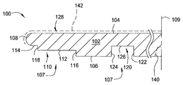
[0013] 도 2는 본 발명의 일부 실시예들에 따라 도 1의 예시적 셔터 디스크의 중심선으로부터 부분 단면도이다.
[0014] 도 3은 본 발명의 일부 실시예들에 따라 셔터 디스크의 다른 실시예의 중심선으로부터 부분 단면도이다.
[0015] 도 4는 본 발명의 일부 실시예들과 관계되어 사용하기 적절한 예시적 프로세싱 챔버의 개략도이다.
Claims (15)
- 상단 표면;
바닥 표면;
상기 상단 표면과 상기 바닥 표면 사이에 위치된 외경을 포함하는
디스크-형상 본체; 및
상기 바닥 표면을 상기 외경에 연결하는 이중 스텝부를 포함하는
셔터 디스크.
- 제 1 항에 있어서,
상기 이중 스텝부는 외부 스텝 및 내부 스텝을 더 포함하며, 상기 외부 스텝이 상기 내부 스텝보다 상기 본체 내로 더 연장되는
셔터 디스크.
- 제 2 항에 있어서,
상기 본체는 상기 외부 스텝부를 상기 내부 스텝에 연결하는 외벽을 더 포함하며, 상기 외벽이 상기 본체의 중심선에 실질적으로 평행한
셔터 디스크.
- 제 3 항에 있어서,
상기 내부 스텝부 및 상기 외부 스텝부는 상기 본체의 중심선에 실질적으로 평행한
셔터 디스크.
- 제 1 항에 있어서,
상기 본체가 상기 이중 스텝부의 방사상 내측으로 배치된 상기 바닥 표면에 형성된 환형 그루브를 더 포함하는
셔터 디스크.
- 제 5 항에 있어서,
상기 이중 스텝부는 외부 스텝부 및 내부 스텝부를 더 포함하며, 상기 외부 스텝부가 상기 내부 스텝부보다 상기 본체내로 더 연장되지만 상기 환형 그루브보다 더 적게 연장되는
셔터 디스크.
- 제 1 항에 있어서,
상기 본체의 바닥 표면에 형성된 막힘 홀을 더 포함하며, 상기 막힘 홀의 중심선이 상기 본체의 중심선과 동일 선상인
셔터 디스크.
- 제 1 항에 있어서,
상기 본체는 알루미늄, 알루미늄 합금, 알루미늄 실리콘 합금, 금속 복합 재료, 및 알루미늄실리콘(AISi) 중 하나 이상으로부터 제조되며, 상기 본체의 상단 표면이 알루미늄 코팅에 의해 코팅되는
셔터 디스크.
- 제 1 항에 있어서,
상기 본체는 상기 외경을 상기 상단 표면에 커플링하는 경사 표면을 더 포함하는
셔터 디스크.
- 제 9 항에 있어서,
상기 본체는 상기 본체의 바닥 표면에 형성된 막힘 홀을 더 포함하고, 상기 막힘 홀의 중심선이 상기 본체의 중심선과 동일 선상인
셔터 디스크.
- 제 1 항에 있어서,
상기 이중 스텝부는 외부 스텝 및 내부 스텝을 더 포함하며, 상기 내부 스텝부는 상기 외부 스텝부보다 상기 본체 내로 더 연장되는
셔터 디스크.
- 디스크-형상 본체를 포함하고,
상기 본체는
상단 표면;
바닥 표면;
상기 상단 표면과 상기 바닥 표면 사이에 위치된 외경; 상기 바닥 표면 상에 형성된 외부 스텝부;
상기 외부 스텝부의 내측으로 상기 바닥 표면 상에 형성된 내부 스텝부 - 상기 외부 스텝부는 상기 내부 스텝부보다 상기 본체 내로 더 연장됨 - ;
상기 외부 스텝부를 상기 내부 스텝부에 연결하는 외벽 - 상기 외벽은 상기 본체의 중심선에 실질적으로 평행함 - ; 및
상기 내부 스텝부의 방사상 내측으로 배치된 상기 바닥 표면에 형성된 환형 그루브를 포함하는
셔터 디스크.
- 제 12 항에 있어서,
상기 내부 스텝부 내지 상기 외부 스텝부는 상기 본체의 중심선에 실질적으로 평행하고, 그리고 상기 외부 스텝부는 상기 내부 스텝부보다 상기 본체 내로 더 연장되지만 상기 환형 그루브보다 더 적게 연장되는
셔터 디스크.
- 제 13 항에 있어서,
상기 본체는 상기 본체의 바닥 표면에 형성된 막힘 홀을 더 포함하고, 상기 막힘 홀의 중심선이 상기 본체의 중심선과 동일 선상인
셔터 디스크.
- 제 13 항에 있어서,
상기 본체는 알루미늄, 알루미늄 합금, 알루미늄 실리콘 합금, 금속 복합 재료, 및 알루미늄 실리콘 (AISi)중 하나 이상으로부터 제조되며, 상기 상단 표면은 약 600 내지 약 800 Ra 사이까지의 평균 거칠기를 가지며 트윈-아크-스프레이 알루미늄 코팅에 의해 코팅되는
셔터 디스크.
Applications Claiming Priority (4)
| Application Number | Priority Date | Filing Date | Title |
|---|---|---|---|
| US9909008P | 2008-09-22 | 2008-09-22 | |
| US61/099,090 | 2008-09-22 | ||
| US12/542,501 US8807075B2 (en) | 2008-09-22 | 2009-08-17 | Shutter disk having a tuned coefficient of thermal expansion |
| US12/542,501 | 2009-08-17 |
Related Child Applications (1)
| Application Number | Title | Priority Date | Filing Date |
|---|---|---|---|
| KR1020167019848A Division KR101888830B1 (ko) | 2008-09-22 | 2009-09-21 | 물리 기상 증착 챔버용 셔터 디스크 |
Publications (2)
| Publication Number | Publication Date |
|---|---|
| KR20110082005A true KR20110082005A (ko) | 2011-07-15 |
| KR101643133B1 KR101643133B1 (ko) | 2016-07-27 |
Family
ID=42036321
Family Applications (2)
| Application Number | Title | Priority Date | Filing Date |
|---|---|---|---|
| KR1020117009308A Active KR101643133B1 (ko) | 2008-09-22 | 2009-09-21 | 물리 기상 증착 챔버용 셔터 디스크 |
| KR1020167019848A Active KR101888830B1 (ko) | 2008-09-22 | 2009-09-21 | 물리 기상 증착 챔버용 셔터 디스크 |
Family Applications After (1)
| Application Number | Title | Priority Date | Filing Date |
|---|---|---|---|
| KR1020167019848A Active KR101888830B1 (ko) | 2008-09-22 | 2009-09-21 | 물리 기상 증착 챔버용 셔터 디스크 |
Country Status (5)
| Country | Link |
|---|---|
| US (1) | US8807075B2 (ko) |
| KR (2) | KR101643133B1 (ko) |
| CN (1) | CN102160146B (ko) |
| TW (1) | TWI484052B (ko) |
| WO (1) | WO2010033904A2 (ko) |
Families Citing this family (11)
| Publication number | Priority date | Publication date | Assignee | Title |
|---|---|---|---|---|
| US9252002B2 (en) | 2012-07-17 | 2016-02-02 | Applied Materials, Inc. | Two piece shutter disk assembly for a substrate process chamber |
| CN103911585A (zh) * | 2013-01-08 | 2014-07-09 | 旭晖应用材料股份有限公司 | 遮罩 |
| US9147558B2 (en) * | 2013-01-16 | 2015-09-29 | Applied Materials, Inc. | Finned shutter disk for a substrate process chamber |
| US9564348B2 (en) * | 2013-03-15 | 2017-02-07 | Applied Materials, Inc. | Shutter blade and robot blade with CTE compensation |
| CN104746034B (zh) * | 2013-12-31 | 2017-09-01 | 北京北方微电子基地设备工艺研究中心有限责任公司 | Pvd腔室遮挡盘检测装置和pvd腔室 |
| JP7404268B2 (ja) | 2018-04-18 | 2023-12-25 | アプライド マテリアルズ インコーポレイテッド | 自己センタリング特徴を有するツーピースシャッタディスクアセンブリ |
| US11251028B2 (en) | 2018-05-12 | 2022-02-15 | Applied Materials, Inc. | Pre-clean chamber with integrated shutter garage |
| CN113924387A (zh) * | 2019-05-22 | 2022-01-11 | 应用材料公司 | 用于高温腐蚀环境的基板支承件盖 |
| US12080571B2 (en) * | 2020-07-08 | 2024-09-03 | Applied Materials, Inc. | Substrate processing module and method of moving a workpiece |
| KR102790387B1 (ko) * | 2020-11-26 | 2025-04-01 | 주식회사 엘지화학 | 배터리 관리 장치 및 방법 |
| US12338527B2 (en) * | 2021-09-03 | 2025-06-24 | Applied Materials, Inc. | Shutter disk for physical vapor deposition (PVD) chamber |
Citations (4)
| Publication number | Priority date | Publication date | Assignee | Title |
|---|---|---|---|---|
| US3381660A (en) * | 1967-06-09 | 1968-05-07 | Nat Res Corp | Vapor deposition apparatus including pivoted shutters |
| US20040182698A1 (en) * | 2002-02-20 | 2004-09-23 | Applied Materials, Inc. | Shutter disk and blade for physical vapor deposition chamber |
| US20050051517A1 (en) * | 2003-08-12 | 2005-03-10 | Oehrlein Gottlieb S. | Method and system for nanoscale plasma processing of objects |
| US20070258075A1 (en) * | 2006-05-03 | 2007-11-08 | Samsung Electronics Co., Ltd. | Apparatus for processing a semiconductor wafer and method of forming the same |
Family Cites Families (20)
| Publication number | Priority date | Publication date | Assignee | Title |
|---|---|---|---|---|
| US5140482A (en) * | 1990-10-04 | 1992-08-18 | Hitachi, Ltd. | Guide arm with affixed printed circuit board for magnetic disk drive |
| US5223112A (en) | 1991-04-30 | 1993-06-29 | Applied Materials, Inc. | Removable shutter apparatus for a semiconductor process chamber |
| US6190513B1 (en) * | 1997-05-14 | 2001-02-20 | Applied Materials, Inc. | Darkspace shield for improved RF transmission in inductively coupled plasma sources for sputter deposition |
| US6162297A (en) * | 1997-09-05 | 2000-12-19 | Applied Materials, Inc. | Embossed semiconductor fabrication parts |
| TW498544B (en) | 2000-03-13 | 2002-08-11 | Tadahiro Ohmi | Flash memory device, manufacturing and its dielectric film formation |
| JP3860954B2 (ja) * | 2000-07-07 | 2006-12-20 | 株式会社日立グローバルストレージテクノロジーズ | リアルタイムパーティクルフィルタを具備したプラズマ処理装置 |
| US20020090464A1 (en) | 2000-11-28 | 2002-07-11 | Mingwei Jiang | Sputter chamber shield |
| US6440879B1 (en) | 2001-01-05 | 2002-08-27 | Integrated Device Technology, Inc. | Physical vapor deposition apparatus with modified shutter disk and cover ring |
| US6669829B2 (en) | 2002-02-20 | 2003-12-30 | Applied Materials, Inc. | Shutter disk and blade alignment sensor |
| US20050153059A1 (en) | 2002-02-28 | 2005-07-14 | Yasuhiro Wakizaka | Partial plating method, partially-plated resin base, method for manufacturing multilayered circuit board |
| US20050064247A1 (en) * | 2003-06-25 | 2005-03-24 | Ajit Sane | Composite refractory metal carbide coating on a substrate and method for making thereof |
| TWI356100B (en) * | 2003-07-24 | 2012-01-11 | Applied Materials Inc | Shutter disk and blade for physical vapor depositi |
| US6847057B1 (en) * | 2003-08-01 | 2005-01-25 | Lumileds Lighting U.S., Llc | Semiconductor light emitting devices |
| US20050048876A1 (en) * | 2003-09-02 | 2005-03-03 | Applied Materials, Inc. | Fabricating and cleaning chamber components having textured surfaces |
| TWI270162B (en) * | 2004-01-27 | 2007-01-01 | Macronix Int Co Ltd | Physical vapor deposition process and apparatus thereof |
| JP4527431B2 (ja) * | 2004-04-08 | 2010-08-18 | 東京エレクトロン株式会社 | プラズマ処理装置 |
| US8460519B2 (en) | 2005-10-28 | 2013-06-11 | Applied Materials Inc. | Protective offset sputtering |
| JP5183058B2 (ja) * | 2006-07-20 | 2013-04-17 | アプライド マテリアルズ インコーポレイテッド | 急速温度勾配コントロールによる基板処理 |
| CN101179005B (zh) * | 2006-11-10 | 2010-10-27 | Tes股份有限公司 | 排气系统及使用此系统制造薄膜的半导体制造装置与方法 |
| US7795054B2 (en) * | 2006-12-08 | 2010-09-14 | Samsung Led Co., Ltd. | Vertical structure LED device and method of manufacturing the same |
-
2009
- 2009-08-17 US US12/542,501 patent/US8807075B2/en active Active
- 2009-09-21 CN CN2009801380005A patent/CN102160146B/zh active Active
- 2009-09-21 KR KR1020117009308A patent/KR101643133B1/ko active Active
- 2009-09-21 WO PCT/US2009/057663 patent/WO2010033904A2/en not_active Ceased
- 2009-09-21 KR KR1020167019848A patent/KR101888830B1/ko active Active
- 2009-09-22 TW TW098131940A patent/TWI484052B/zh active
Patent Citations (4)
| Publication number | Priority date | Publication date | Assignee | Title |
|---|---|---|---|---|
| US3381660A (en) * | 1967-06-09 | 1968-05-07 | Nat Res Corp | Vapor deposition apparatus including pivoted shutters |
| US20040182698A1 (en) * | 2002-02-20 | 2004-09-23 | Applied Materials, Inc. | Shutter disk and blade for physical vapor deposition chamber |
| US20050051517A1 (en) * | 2003-08-12 | 2005-03-10 | Oehrlein Gottlieb S. | Method and system for nanoscale plasma processing of objects |
| US20070258075A1 (en) * | 2006-05-03 | 2007-11-08 | Samsung Electronics Co., Ltd. | Apparatus for processing a semiconductor wafer and method of forming the same |
Also Published As
| Publication number | Publication date |
|---|---|
| CN102160146B (zh) | 2013-12-25 |
| US8807075B2 (en) | 2014-08-19 |
| WO2010033904A2 (en) | 2010-03-25 |
| US20100071625A1 (en) | 2010-03-25 |
| KR101888830B1 (ko) | 2018-09-20 |
| TW201024432A (en) | 2010-07-01 |
| CN102160146A (zh) | 2011-08-17 |
| TWI484052B (zh) | 2015-05-11 |
| WO2010033904A3 (en) | 2010-07-22 |
| KR20160090402A (ko) | 2016-07-29 |
| KR101643133B1 (ko) | 2016-07-27 |
Similar Documents
| Publication | Publication Date | Title |
|---|---|---|
| US11049761B2 (en) | Shutter disk for physical vapor deposition chamber | |
| KR101888830B1 (ko) | 물리 기상 증착 챔버용 셔터 디스크 | |
| CN112088227B (zh) | 具有整合遮件库的预清洁腔室 | |
| US9252002B2 (en) | Two piece shutter disk assembly for a substrate process chamber | |
| US9689070B2 (en) | Deposition ring and electrostatic chuck for physical vapor deposition chamber | |
| US20080141942A1 (en) | Non-contact process kit | |
| KR101724269B1 (ko) | 기판 프로세스 챔버를 위한 핀형 셔터 디스크 | |
| KR20090094144A (ko) | 비접촉 프로세스 키트 | |
| TWI829685B (zh) | 具有自定心特徵的兩件式快門盤組件 | |
| KR102157819B1 (ko) | 열 최적화 링들 | |
| CN104641016A (zh) | 用于定向材料沉积的pvd设备、方法和工件 |
Legal Events
| Date | Code | Title | Description |
|---|---|---|---|
| PA0105 | International application |
St.27 status event code: A-0-1-A10-A15-nap-PA0105 |
|
| PG1501 | Laying open of application |
St.27 status event code: A-1-1-Q10-Q12-nap-PG1501 |
|
| R17-X000 | Change to representative recorded |
St.27 status event code: A-3-3-R10-R17-oth-X000 |
|
| P11-X000 | Amendment of application requested |
St.27 status event code: A-2-2-P10-P11-nap-X000 |
|
| P13-X000 | Application amended |
St.27 status event code: A-2-2-P10-P13-nap-X000 |
|
| A201 | Request for examination | ||
| PA0201 | Request for examination |
St.27 status event code: A-1-2-D10-D11-exm-PA0201 |
|
| A302 | Request for accelerated examination | ||
| E13-X000 | Pre-grant limitation requested |
St.27 status event code: A-2-3-E10-E13-lim-X000 |
|
| P11-X000 | Amendment of application requested |
St.27 status event code: A-2-2-P10-P11-nap-X000 |
|
| P13-X000 | Application amended |
St.27 status event code: A-2-2-P10-P13-nap-X000 |
|
| PA0302 | Request for accelerated examination |
St.27 status event code: A-1-2-D10-D17-exm-PA0302 St.27 status event code: A-1-2-D10-D16-exm-PA0302 |
|
| E902 | Notification of reason for refusal | ||
| PE0902 | Notice of grounds for rejection |
St.27 status event code: A-1-2-D10-D21-exm-PE0902 |
|
| P11-X000 | Amendment of application requested |
St.27 status event code: A-2-2-P10-P11-nap-X000 |
|
| P13-X000 | Application amended |
St.27 status event code: A-2-2-P10-P13-nap-X000 |
|
| E701 | Decision to grant or registration of patent right | ||
| PE0701 | Decision of registration |
St.27 status event code: A-1-2-D10-D22-exm-PE0701 |
|
| A107 | Divisional application of patent | ||
| PA0104 | Divisional application for international application |
St.27 status event code: A-0-1-A10-A18-div-PA0104 St.27 status event code: A-0-1-A10-A16-div-PA0104 |
|
| GRNT | Written decision to grant | ||
| PR0701 | Registration of establishment |
St.27 status event code: A-2-4-F10-F11-exm-PR0701 |
|
| PR1002 | Payment of registration fee |
St.27 status event code: A-2-2-U10-U12-oth-PR1002 Fee payment year number: 1 |
|
| PG1601 | Publication of registration |
St.27 status event code: A-4-4-Q10-Q13-nap-PG1601 |
|
| PR1001 | Payment of annual fee |
St.27 status event code: A-4-4-U10-U11-oth-PR1001 Fee payment year number: 4 |
|
| PR1001 | Payment of annual fee |
St.27 status event code: A-4-4-U10-U11-oth-PR1001 Fee payment year number: 5 |
|
| PR1001 | Payment of annual fee |
St.27 status event code: A-4-4-U10-U11-oth-PR1001 Fee payment year number: 6 |
|
| PR1001 | Payment of annual fee |
St.27 status event code: A-4-4-U10-U11-oth-PR1001 Fee payment year number: 7 |
|
| PR1001 | Payment of annual fee |
St.27 status event code: A-4-4-U10-U11-oth-PR1001 Fee payment year number: 8 |
|
| P22-X000 | Classification modified |
St.27 status event code: A-4-4-P10-P22-nap-X000 |
|
| PR1001 | Payment of annual fee |
St.27 status event code: A-4-4-U10-U11-oth-PR1001 Fee payment year number: 9 |
|
| PR1001 | Payment of annual fee |
St.27 status event code: A-4-4-U10-U11-oth-PR1001 Fee payment year number: 10 |
|
| P22-X000 | Classification modified |
St.27 status event code: A-4-4-P10-P22-nap-X000 |