KR20120002890A - 발광 유닛 - Google Patents
발광 유닛 Download PDFInfo
- Publication number
- KR20120002890A KR20120002890A KR1020100063630A KR20100063630A KR20120002890A KR 20120002890 A KR20120002890 A KR 20120002890A KR 1020100063630 A KR1020100063630 A KR 1020100063630A KR 20100063630 A KR20100063630 A KR 20100063630A KR 20120002890 A KR20120002890 A KR 20120002890A
- Authority
- KR
- South Korea
- Prior art keywords
- light emitting
- light
- emitting layer
- substrate
- pattern
- Prior art date
- Legal status (The legal status is an assumption and is not a legal conclusion. Google has not performed a legal analysis and makes no representation as to the accuracy of the status listed.)
- Granted
Links
Images





Classifications
-
- H—ELECTRICITY
- H10—SEMICONDUCTOR DEVICES; ELECTRIC SOLID-STATE DEVICES NOT OTHERWISE PROVIDED FOR
- H10K—ORGANIC ELECTRIC SOLID-STATE DEVICES
- H10K50/00—Organic light-emitting devices
- H10K50/10—OLEDs or polymer light-emitting diodes [PLED]
- H10K50/11—OLEDs or polymer light-emitting diodes [PLED] characterised by the electroluminescent [EL] layers
- H10K50/115—OLEDs or polymer light-emitting diodes [PLED] characterised by the electroluminescent [EL] layers comprising active inorganic nanostructures, e.g. luminescent quantum dots
-
- G—PHYSICS
- G09—EDUCATION; CRYPTOGRAPHY; DISPLAY; ADVERTISING; SEALS
- G09F—DISPLAYING; ADVERTISING; SIGNS; LABELS OR NAME-PLATES; SEALS
- G09F13/00—Illuminated signs; Luminous advertising
- G09F13/04—Signs, boards or panels, illuminated from behind the insignia
- G09F13/12—Signs, boards or panels, illuminated from behind the insignia using a transparent mirror or other light reflecting surface transparent to transmitted light whereby a sign, symbol, picture or other is visible only when illuminated
-
- G—PHYSICS
- G09—EDUCATION; CRYPTOGRAPHY; DISPLAY; ADVERTISING; SEALS
- G09F—DISPLAYING; ADVERTISING; SIGNS; LABELS OR NAME-PLATES; SEALS
- G09F13/00—Illuminated signs; Luminous advertising
- G09F13/20—Illuminated signs; Luminous advertising with luminescent surfaces or parts
-
- G—PHYSICS
- G09—EDUCATION; CRYPTOGRAPHY; DISPLAY; ADVERTISING; SEALS
- G09F—DISPLAYING; ADVERTISING; SIGNS; LABELS OR NAME-PLATES; SEALS
- G09F13/00—Illuminated signs; Luminous advertising
- G09F13/20—Illuminated signs; Luminous advertising with luminescent surfaces or parts
- G09F13/22—Illuminated signs; Luminous advertising with luminescent surfaces or parts electroluminescent
- G09F2013/222—Illuminated signs; Luminous advertising with luminescent surfaces or parts electroluminescent with LEDs
Landscapes
- Physics & Mathematics (AREA)
- Engineering & Computer Science (AREA)
- General Physics & Mathematics (AREA)
- Theoretical Computer Science (AREA)
- Chemical & Material Sciences (AREA)
- Crystallography & Structural Chemistry (AREA)
- Inorganic Chemistry (AREA)
- Nanotechnology (AREA)
- Optics & Photonics (AREA)
- Illuminated Signs And Luminous Advertising (AREA)
Abstract
Description
도 2는 도 1의 II-II선을 따라 절단한 단면도이다.
도 3은 양자점을 구성을 보여주는 도면이다.
도 4는 블랙층이 더 형성된 발광 유닛을 설명하는 도면이다.
도 5는 꽃무늬가 그려진 냉장고의 도어 부분을 보여주는 도면이다.
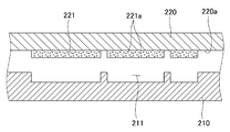
도 6은 도 5의 VI-VI 선을 따라 절단한 단면도이다.
도 7은 도 6에 도시한 발광층의 패턴을 보여주는 도면이다.
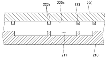
도 8은 도 6과 다른 형태의 발광층을 설명하는 단면도이다.
도 9는 도 8에 도시한 발광층의 패턴을 보여주는 도면이다.
도 10은 광원부가 더 형성된 것을 설명하는 도면이다.
도 11은 발광층에서 빛의 이동 경로를 설명하는 도면이다.
도 12는 발광유닛이 적용된 텔레비젼을 보여주는 도면이다.
도 13은 도 12의 XIII-XIII 선을 따라 절단한 단면도이다.
도 14는 발광층의 패턴을 보여주는 도면이다.
Claims (10)
- 제1 기판과,
상기 제1 기판 위에 형성되며, 빛에 반응해서 발광하는 소자가 포함된 발광층이 도안을 이루고 있는 발광 유닛. - 제1항에 있어서,
상기 발광소자는 II족 화합물 반도체, III족 화합물 반도체, V족 화합물 반도체, VI족 화합물 반도체 중에서도 적어도 2종의 반도체가 결합된 양자점(quantumn dot)인 발광 유닛. - 제2항에 있어서,
상기 양자점은, 코어부가 CdSe, InGaP, InP 중 적어도 하나를 포함하고, 껍질부는 ZnS, CuZnS 중 적어도 하나를 포함하는 발광 유닛. - 제2항에 있어서,
상기 제1 기판과 상기 발광층은 투명하고, 상기 발광층은 투과율이 70% 이상 85% 이하인 발광 유닛. - 제4항에 있어서,
상기 양자점은 상기 발광층에 0.5(wt%) ∼ 2.5(wt%) 포함되어 있는 발광 유닛. - 제2항에 있어서,
상기 발광층은 서로 다른 색상의 빛을 내는 적어도 2 이상의 양자점이 각각 포함된 제1 및 제2 발광층을 포함하는 발광 유닛. - 제2항에 있어서,
상기 양자점은 가시광과 자외선의 경계 영역인 430(mm) ∼ 450(nm) 파장의 빛에 반응해서 발광하는 발광 유닛. - 제1항에 있어서,
상기 발광층을 덮고 있으며, 상기 발광층이 보이지 않도록 하는 블랙층이 더 형성되어 있는 발광 유닛. - 제1항에 있어서,
상기 제1 기판과 마주하며, 상기 도안과 짝을 이루는 패턴이 형성되어 있는 제2 기판을 더 포함하는 발광 유닛. - 제9항에 있어서,
상기 패턴은 상기 제2 기판의 표면에 그루브를 형성해서 만들어진 발광 유닛.
Priority Applications (1)
| Application Number | Priority Date | Filing Date | Title |
|---|---|---|---|
| KR1020100063630A KR101760007B1 (ko) | 2010-07-01 | 2010-07-01 | 발광 유닛 |
Applications Claiming Priority (1)
| Application Number | Priority Date | Filing Date | Title |
|---|---|---|---|
| KR1020100063630A KR101760007B1 (ko) | 2010-07-01 | 2010-07-01 | 발광 유닛 |
Publications (2)
| Publication Number | Publication Date |
|---|---|
| KR20120002890A true KR20120002890A (ko) | 2012-01-09 |
| KR101760007B1 KR101760007B1 (ko) | 2017-07-31 |
Family
ID=45610083
Family Applications (1)
| Application Number | Title | Priority Date | Filing Date |
|---|---|---|---|
| KR1020100063630A Expired - Fee Related KR101760007B1 (ko) | 2010-07-01 | 2010-07-01 | 발광 유닛 |
Country Status (1)
| Country | Link |
|---|---|
| KR (1) | KR101760007B1 (ko) |
Cited By (1)
| Publication number | Priority date | Publication date | Assignee | Title |
|---|---|---|---|---|
| WO2014064537A3 (en) * | 2012-10-04 | 2014-10-23 | Nanoco Technologies, Ltd. | Illuminated signage using quantum dots |
Family Cites Families (1)
| Publication number | Priority date | Publication date | Assignee | Title |
|---|---|---|---|---|
| US8836212B2 (en) * | 2007-01-11 | 2014-09-16 | Qd Vision, Inc. | Light emissive printed article printed with quantum dot ink |
-
2010
- 2010-07-01 KR KR1020100063630A patent/KR101760007B1/ko not_active Expired - Fee Related
Cited By (3)
| Publication number | Priority date | Publication date | Assignee | Title |
|---|---|---|---|---|
| WO2014064537A3 (en) * | 2012-10-04 | 2014-10-23 | Nanoco Technologies, Ltd. | Illuminated signage using quantum dots |
| CN104838437A (zh) * | 2012-10-04 | 2015-08-12 | 纳米技术有限公司 | 使用量子点的照明标识 |
| US9548009B2 (en) | 2012-10-04 | 2017-01-17 | Nanoco Technologies Ltd. | Illuminated signage using quantum dots |
Also Published As
| Publication number | Publication date |
|---|---|
| KR101760007B1 (ko) | 2017-07-31 |
Similar Documents
| Publication | Publication Date | Title |
|---|---|---|
| US10851965B2 (en) | Resin component and display device using the same | |
| KR100436925B1 (ko) | 모자 | |
| US20180149780A1 (en) | Reflective light-emitting film, preparation method and use thereof | |
| TWM472244U (zh) | 觸控面板 | |
| CN115056563A (zh) | 装饰膜片、发光模组以及电子设备 | |
| US20100108247A1 (en) | Method and Apparatus for a Retro-reflective Material | |
| CN115891375A (zh) | 一种皮革表面透光的汽车发光内饰件及其生产方法 | |
| KR101714309B1 (ko) | 외장재 | |
| CN103565342B (zh) | 马桶座 | |
| KR20120002890A (ko) | 발광 유닛 | |
| JP2018018063A (ja) | 夜光性装飾物 | |
| KR101581383B1 (ko) | 씨스루 효과를 갖는 광발열 패딩자켓 | |
| CN204845049U (zh) | 一种自反光珠片 | |
| KR101896577B1 (ko) | 조광 표시 장치의 제조 방법 | |
| CN218384378U (zh) | 显示设备 | |
| CN108711381A (zh) | 一种logo指示灯结构 | |
| JP5128763B2 (ja) | 発光性表示体及びその製造方法 | |
| KR20210064703A (ko) | 발광장치가 구비된 와펜 패치 | |
| TWI675613B (zh) | 殼體、該殼體的製備方法及應用該殼體的電子裝置 | |
| CN110598660A (zh) | 一种实现指纹传感器表面发光图案的方法 | |
| TWI356666B (en) | Decoration plate and method of making thereof | |
| KR101397550B1 (ko) | 부분 투광성 패턴체 제조 방법 및 그 부분 투광성 패턴체 | |
| CN220105326U (zh) | 光学薄膜及显示面板 | |
| JP2011068123A (ja) | 成形品 | |
| TW201331898A (zh) | 具發光效果之複合銘版結構 |
Legal Events
| Date | Code | Title | Description |
|---|---|---|---|
| PA0109 | Patent application |
St.27 status event code: A-0-1-A10-A12-nap-PA0109 |
|
| PG1501 | Laying open of application |
St.27 status event code: A-1-1-Q10-Q12-nap-PG1501 |
|
| A201 | Request for examination | ||
| P11-X000 | Amendment of application requested |
St.27 status event code: A-2-2-P10-P11-nap-X000 |
|
| P13-X000 | Application amended |
St.27 status event code: A-2-2-P10-P13-nap-X000 |
|
| PA0201 | Request for examination |
St.27 status event code: A-1-2-D10-D11-exm-PA0201 |
|
| P11-X000 | Amendment of application requested |
St.27 status event code: A-2-2-P10-P11-nap-X000 |
|
| P13-X000 | Application amended |
St.27 status event code: A-2-2-P10-P13-nap-X000 |
|
| PN2301 | Change of applicant |
St.27 status event code: A-3-3-R10-R13-asn-PN2301 St.27 status event code: A-3-3-R10-R11-asn-PN2301 |
|
| P22-X000 | Classification modified |
St.27 status event code: A-2-2-P10-P22-nap-X000 |
|
| D13-X000 | Search requested |
St.27 status event code: A-1-2-D10-D13-srh-X000 |
|
| D14-X000 | Search report completed |
St.27 status event code: A-1-2-D10-D14-srh-X000 |
|
| E902 | Notification of reason for refusal | ||
| PE0902 | Notice of grounds for rejection |
St.27 status event code: A-1-2-D10-D21-exm-PE0902 |
|
| E13-X000 | Pre-grant limitation requested |
St.27 status event code: A-2-3-E10-E13-lim-X000 |
|
| P11-X000 | Amendment of application requested |
St.27 status event code: A-2-2-P10-P11-nap-X000 |
|
| P13-X000 | Application amended |
St.27 status event code: A-2-2-P10-P13-nap-X000 |
|
| E902 | Notification of reason for refusal | ||
| PE0902 | Notice of grounds for rejection |
St.27 status event code: A-1-2-D10-D21-exm-PE0902 |
|
| E13-X000 | Pre-grant limitation requested |
St.27 status event code: A-2-3-E10-E13-lim-X000 |
|
| P11-X000 | Amendment of application requested |
St.27 status event code: A-2-2-P10-P11-nap-X000 |
|
| P13-X000 | Application amended |
St.27 status event code: A-2-2-P10-P13-nap-X000 |
|
| E701 | Decision to grant or registration of patent right | ||
| PE0701 | Decision of registration |
St.27 status event code: A-1-2-D10-D22-exm-PE0701 |
|
| GRNT | Written decision to grant | ||
| PR0701 | Registration of establishment |
St.27 status event code: A-2-4-F10-F11-exm-PR0701 |
|
| PR1002 | Payment of registration fee |
St.27 status event code: A-2-2-U10-U11-oth-PR1002 Fee payment year number: 1 |
|
| PG1601 | Publication of registration |
St.27 status event code: A-4-4-Q10-Q13-nap-PG1601 |
|
| PN2301 | Change of applicant |
St.27 status event code: A-5-5-R10-R13-asn-PN2301 St.27 status event code: A-5-5-R10-R11-asn-PN2301 |
|
| FPAY | Annual fee payment |
Payment date: 20200624 Year of fee payment: 4 |
|
| PR1001 | Payment of annual fee |
St.27 status event code: A-4-4-U10-U11-oth-PR1001 Fee payment year number: 4 |
|
| FPAY | Annual fee payment |
Payment date: 20210618 Year of fee payment: 5 |
|
| PR1001 | Payment of annual fee |
St.27 status event code: A-4-4-U10-U11-oth-PR1001 Fee payment year number: 5 |
|
| FPAY | Annual fee payment |
Payment date: 20220622 Year of fee payment: 6 |
|
| PR1001 | Payment of annual fee |
St.27 status event code: A-4-4-U10-U11-oth-PR1001 Fee payment year number: 6 |
|
| P22-X000 | Classification modified |
St.27 status event code: A-4-4-P10-P22-nap-X000 |
|
| P22-X000 | Classification modified |
St.27 status event code: A-4-4-P10-P22-nap-X000 |
|
| PC1903 | Unpaid annual fee |
St.27 status event code: A-4-4-U10-U13-oth-PC1903 Not in force date: 20230715 Payment event data comment text: Termination Category : DEFAULT_OF_REGISTRATION_FEE |
|
| PC1903 | Unpaid annual fee |
St.27 status event code: N-4-6-H10-H13-oth-PC1903 Ip right cessation event data comment text: Termination Category : DEFAULT_OF_REGISTRATION_FEE Not in force date: 20230715 |
|
| P22-X000 | Classification modified |
St.27 status event code: A-4-4-P10-P22-nap-X000 |
|
| P22-X000 | Classification modified |
St.27 status event code: A-4-4-P10-P22-nap-X000 |