KR20120003000A - Dhlfc 물질에 기초한 광 메모리 장치 및 그 제조 방법 - Google Patents
Dhlfc 물질에 기초한 광 메모리 장치 및 그 제조 방법 Download PDFInfo
- Publication number
- KR20120003000A KR20120003000A KR1020117025406A KR20117025406A KR20120003000A KR 20120003000 A KR20120003000 A KR 20120003000A KR 1020117025406 A KR1020117025406 A KR 1020117025406A KR 20117025406 A KR20117025406 A KR 20117025406A KR 20120003000 A KR20120003000 A KR 20120003000A
- Authority
- KR
- South Korea
- Prior art keywords
- glass substrate
- substrate
- cell structure
- memory device
- optical memory
- Prior art date
- Legal status (The legal status is an assumption and is not a legal conclusion. Google has not performed a legal analysis and makes no representation as to the accuracy of the status listed.)
- Granted
Links
Images


Classifications
-
- C—CHEMISTRY; METALLURGY
- C09—DYES; PAINTS; POLISHES; NATURAL RESINS; ADHESIVES; COMPOSITIONS NOT OTHERWISE PROVIDED FOR; APPLICATIONS OF MATERIALS NOT OTHERWISE PROVIDED FOR
- C09K—MATERIALS FOR MISCELLANEOUS APPLICATIONS, NOT PROVIDED FOR ELSEWHERE
- C09K19/00—Liquid crystal materials
- C09K19/02—Liquid crystal materials characterised by optical, electrical or physical properties of the components, in general
- C09K19/0225—Ferroelectric
-
- G—PHYSICS
- G02—OPTICS
- G02F—OPTICAL DEVICES OR ARRANGEMENTS FOR THE CONTROL OF LIGHT BY MODIFICATION OF THE OPTICAL PROPERTIES OF THE MEDIA OF THE ELEMENTS INVOLVED THEREIN; NON-LINEAR OPTICS; FREQUENCY-CHANGING OF LIGHT; OPTICAL LOGIC ELEMENTS; OPTICAL ANALOGUE/DIGITAL CONVERTERS
- G02F1/00—Devices or arrangements for the control of the intensity, colour, phase, polarisation or direction of light arriving from an independent light source, e.g. switching, gating or modulating; Non-linear optics
- G02F1/01—Devices or arrangements for the control of the intensity, colour, phase, polarisation or direction of light arriving from an independent light source, e.g. switching, gating or modulating; Non-linear optics for the control of the intensity, phase, polarisation or colour
- G02F1/13—Devices or arrangements for the control of the intensity, colour, phase, polarisation or direction of light arriving from an independent light source, e.g. switching, gating or modulating; Non-linear optics for the control of the intensity, phase, polarisation or colour based on liquid crystals, e.g. single liquid crystal display cells
- G02F1/137—Devices or arrangements for the control of the intensity, colour, phase, polarisation or direction of light arriving from an independent light source, e.g. switching, gating or modulating; Non-linear optics for the control of the intensity, phase, polarisation or colour based on liquid crystals, e.g. single liquid crystal display cells characterised by the electro-optical or magneto-optical effect, e.g. field-induced phase transition, orientation effect, guest-host interaction or dynamic scattering
- G02F1/139—Devices or arrangements for the control of the intensity, colour, phase, polarisation or direction of light arriving from an independent light source, e.g. switching, gating or modulating; Non-linear optics for the control of the intensity, phase, polarisation or colour based on liquid crystals, e.g. single liquid crystal display cells characterised by the electro-optical or magneto-optical effect, e.g. field-induced phase transition, orientation effect, guest-host interaction or dynamic scattering based on orientation effects in which the liquid crystal remains transparent
- G02F1/141—Devices or arrangements for the control of the intensity, colour, phase, polarisation or direction of light arriving from an independent light source, e.g. switching, gating or modulating; Non-linear optics for the control of the intensity, phase, polarisation or colour based on liquid crystals, e.g. single liquid crystal display cells characterised by the electro-optical or magneto-optical effect, e.g. field-induced phase transition, orientation effect, guest-host interaction or dynamic scattering based on orientation effects in which the liquid crystal remains transparent using ferroelectric liquid crystals
-
- G—PHYSICS
- G11—INFORMATION STORAGE
- G11C—STATIC STORES
- G11C11/00—Digital stores characterised by the use of particular electric or magnetic storage elements; Storage elements therefor
- G11C11/21—Digital stores characterised by the use of particular electric or magnetic storage elements; Storage elements therefor using electric elements
- G11C11/22—Digital stores characterised by the use of particular electric or magnetic storage elements; Storage elements therefor using electric elements using ferroelectric elements
Landscapes
- Chemical & Material Sciences (AREA)
- Engineering & Computer Science (AREA)
- Crystallography & Structural Chemistry (AREA)
- Materials Engineering (AREA)
- Organic Chemistry (AREA)
- Computer Hardware Design (AREA)
- Physics & Mathematics (AREA)
- Nonlinear Science (AREA)
- Liquid Crystal (AREA)
- General Physics & Mathematics (AREA)
- Optics & Photonics (AREA)
Abstract
Description
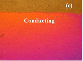
도 2는 파형 발생기(HP 33120A Arbitrary Waveform Generator)의 진폭 변조 설비를 사용하여 정사각 지연파(square delayed pulse)를 인가하여 광 현미경 상에 장착된 포토다이오드를 거쳐 전환된 후 얻어진 광 투과의 전기 신호이다. CH1:8.000V/DIV는 구동 정사각 전압을 나타내고 CH2:0.050V/DIV는 그 광학적 응답을 나타내며, y축(전압축) 상의 외측 마크는 각 채널에 대한 제로 전압 레벨을 나타낸다. TBA:는 x축 상에서 분할당 시간 스케일을 나타내며, 이것은 양 채널에서 같다. (a) 1㎐는 완전히 안정한 전송을 나타내고, (b) 200㎐는 메모리 전송의 저하(degradation)의 시작을 나타내고, (c) 500㎐는 입력 신호의 끝에서 메모리의 가파른 저하, 즉 응답의 지연을 나타낸다.
도 3은 각각 순수한 DHFLC 및 글리세롤이 혼합된 DHFLC 물질의 인가 전압에 따른 응답 시간의 거동이다. 채워진 정사각형은 순수한 DHFLC 물질의 응답 시간을 나타내는 반면 비워진 정사각형은 글리세롤이 혼합된 DHFLC 물질의 응답 시간을 나타낸다.
Claims (18)
- 공간을 한정하는 밀봉된 셀 구조체로서, 상기 셀 구조체는 투명 기재 상에 형성된 전극들을 구비하는 한 쌍의 상기 투명 기재를 포함하는 밀봉된 셀 구조체; 및
상기 셀 구조체에 의해 한정된 상기 공간 내에 위치하며 나선 변형 강유전성 액정(DHFLC) 및 글리세롤을 포함하는 혼합물로서, 상기 혼합물이 글리세롤을 DHFLC의 3.3~10% 부피비로 포함하는 혼합물을 포함하는 광 메모리 장치. - 제1항에 있어서, 상기 투명 기재가 유리 기재인 광 메모리 장치.
- 제1항에 있어서, 상기 전극은 인듐 주석 산화물, 주석 산화물, 및 아연 산화물로 이루어진 군으로부터 선택된 투명 전도 물질로 만들어진 광 메모리 장치.
- 제1항에 있어서, 상기 투명 기재들이 다른 하나의 기재와 대향하는 적어도 하나의 상기 투명 기재의 표면 상에 형성된 스페이서를 사용하여 서로 미리결정된(predetermined) 거리만큼 유지된 광 메모리 장치.
- 제4항에 있어서, 상기 스페이서의 두께가 1 내지 5㎛ 범위인 광 메모리 장치.
- 제4항에 있어서, 상기 스페이서가 포토리소그래피 기술에 의해 준비된 포토레지스트 필름으로 만들어진 광 메모리 장치.
- 하기 단계를 포함하는 광 메모리 장치의 제조 방법:
투명 기재들 사이에 한정된 공감을 가지며 상기 투명 기재들 상에 전극이 배치된 한 쌍의 상기 투명 기재를 포함하는 셀 구조체를 형성하는 단계;
상기 한정된 공간 내에, 나선 변형 강유전성 액정(DHFLC) 및 글리세롤의 혼합물로서 상기 글리세롤이 DHFLC의 3.3~10% 부피비인 혼합물을 충전하는 단계; 및
상기 셀 구조체를 밀봉(sealing)하고 베이킹(baking)하여 상기 광 메모리 장치를 얻는 단계. - 제7항에 있어서, 상기 투명 기재가 유리 기재인 제조 방법.
- 제7항에 있어서, 상기 셀 구조체가 하기 단계에 의해 형성되는 제조 방법:
한 쌍의 광학적으로 평탄한 유리 기재를 세정 및 건조하는 단계;
상기 건조된 유리 기재를 진공 챔버에서 30분 내지 60분 범위의 시간 동안 100℃-250℃ 범위의 온도로 가열하는 단계; 및
1000Å 내지 2000Å 범위의 두께를 가지는 인듐 주석 산화물(ITO) 박막을 증착함으로써 상기 가열된 유리 기재를 코팅하여 30 내지 500Ω/□의 시트 저항 및 적어도 90%의 광 투과도(optical transmission)를 가지는 코팅된 유리 기재를 얻는 단계. - 제9항에 있어서, 상기 코팅된 유리 기재를 얻고 나서 하기 단계를 더 포함하는 제조 방법:
상기 코팅된 유리 기재를 세제 및 아세톤으로 철저하게 세정하고 이어서 탈이온수에서 린스하고 질소 가스에서 건조하고 패턴을 형성하여 적어도 4.5㎟의 유효 전극 영역을 얻는 단계;
상기 패터닝된 유리 기재를 다시 세정하고 건조하고 이어서 상기 패터닝된 유리 기재를 선택된 폴리머(나일론 6/6)로 200 내지 400Å 두께 범위로 스핀 코팅하는 단계; 및
상기 코팅된 기재를 100℃ 내지 120℃ 범위의 온도에서 30분 내지 45분 범위의 시간 동안 베이킹하고 이어서 상기 폴리머 코팅된 표면을 상기 코팅된 유리 기재의 표면의 원하는 방향으로 러빙(rubbing)하는 단계. - 제10항에 있어서, 하기 단계를 더 포함하는 제조 방법:
상기 베이킹된 기재 중 하나를 스핀 코팅으로 코팅하여 1 내지 5㎛ 범위의 두께를 가지는 스페이서를 얻는 단계; 및
상기 기재 중 하나 위에 퇴적된 포토레지스트 스페이서에서 균일한 셀 갭을 유지하고 패터닝된 ITO 전극을 작은 갭으로 매칭시킴으로써 상기 코팅된 유리 기재를 셀 구조체로 조립(assembling)하는 단계. - 제7항에 있어서, 상기 혼합물을 충전하는 단계가, 상기 셀 구조체에 의해 한정된 상기 공간 내에, 80-100℃ 범위의 온도에서 가열하고 이어서 5℃/시간의 속도로 서냉시킴으로써 진행되는 모세관 작용에 의해, 상기 혼합물을 충전하는 것을 포함하는 제조 방법.
- 제7항에 있어서, 상기 셀 구조체를 밀봉하는 단계가 열가소성 수지 또는 UV 실란트를 열고정함으로써 수행되는 제조 방법.
- 제7항에 있어서, 상기 밀봉된 셀 구조체를 베이킹하는 단계가 상기 셀 구조체를 40 내지 60℃ 범위의 온도에서 1 내지 2시간 범위의 시간 동안 베이킹하는 것을 포함하는 제조 방법.
- 제9항에 있어서, 상기 사용되는 코팅이 인듐 주석 산화물, 주석 산화물, 및 아연 산화물로 이루어진 군으로부터 선택된 제조 방법.
- 제9항에 있어서, 상기 세정용 용액이 크롬산, 트리클로로에틸렌, 메탄올로 이루어진 군으로부터 선택된 제조 방법.
- 제10항에 있어서, 상기 패터닝된 유리 기재를 세정하는 단계가 상기 기재를 실란 용액에 침지(dipping)하는 것을 포함하는 제조 방법.
- 제11항에 있어서, 상기 스페이서가 포토리소그래피 기술에 의해 준비된 포토레지스트 필름으로 만들어지는 제조 방법.
Applications Claiming Priority (3)
| Application Number | Priority Date | Filing Date | Title |
|---|---|---|---|
| IN625DE2009 | 2009-03-27 | ||
| IN625/DEL/2009 | 2009-03-27 | ||
| PCT/IB2010/000683 WO2010109316A1 (en) | 2009-03-27 | 2010-03-26 | Optical memory device based on dhlfc material and method of preparing the same |
Publications (2)
| Publication Number | Publication Date |
|---|---|
| KR20120003000A true KR20120003000A (ko) | 2012-01-09 |
| KR101700922B1 KR101700922B1 (ko) | 2017-01-31 |
Family
ID=42236800
Family Applications (1)
| Application Number | Title | Priority Date | Filing Date |
|---|---|---|---|
| KR1020117025406A Expired - Fee Related KR101700922B1 (ko) | 2009-03-27 | 2010-03-26 | Dhflc 물질에 기초한 광 메모리 장치 및 그 제조 방법 |
Country Status (3)
| Country | Link |
|---|---|
| US (1) | US8994911B2 (ko) |
| KR (1) | KR101700922B1 (ko) |
| WO (1) | WO2010109316A1 (ko) |
Cited By (1)
| Publication number | Priority date | Publication date | Assignee | Title |
|---|---|---|---|---|
| KR20200048990A (ko) * | 2018-10-31 | 2020-05-08 | 재단법인대구경북과학기술원 | 메모리 셀 유닛, 스위칭 저항 메모리 소자 및 이를 포함하는 뇌신경모사 소자 |
Families Citing this family (1)
| Publication number | Priority date | Publication date | Assignee | Title |
|---|---|---|---|---|
| CN111876218B (zh) * | 2020-06-19 | 2022-07-19 | 中国石油化工股份有限公司 | 一种导电型轴承润滑脂组合物及其制备方法 |
Citations (4)
| Publication number | Priority date | Publication date | Assignee | Title |
|---|---|---|---|---|
| US4954985A (en) * | 1987-05-09 | 1990-09-04 | Semiconductor Energy Laboratory Co., Ltd. | Ferroelectric liquid crystal data storage card |
| US5316806A (en) * | 1990-06-12 | 1994-05-31 | Canon Kabushiki Kaisha | Information memory medium and information recording/holding process making use of the medium |
| US5539555A (en) * | 1990-07-20 | 1996-07-23 | Displaytech, Inc. | High contrast distorted helex effect electro-optic devices and tight ferroelectric pitch ferroelectric liquid crystal compositions useful therein |
| KR20010029416A (ko) * | 1999-09-16 | 2001-04-06 | 수바람 엔.알. | 폴리머가 코팅된 장수명 광메모리 장치의 제조방법 |
-
2010
- 2010-03-26 WO PCT/IB2010/000683 patent/WO2010109316A1/en not_active Ceased
- 2010-03-26 KR KR1020117025406A patent/KR101700922B1/ko not_active Expired - Fee Related
- 2010-03-26 US US13/260,509 patent/US8994911B2/en not_active Expired - Fee Related
Patent Citations (4)
| Publication number | Priority date | Publication date | Assignee | Title |
|---|---|---|---|---|
| US4954985A (en) * | 1987-05-09 | 1990-09-04 | Semiconductor Energy Laboratory Co., Ltd. | Ferroelectric liquid crystal data storage card |
| US5316806A (en) * | 1990-06-12 | 1994-05-31 | Canon Kabushiki Kaisha | Information memory medium and information recording/holding process making use of the medium |
| US5539555A (en) * | 1990-07-20 | 1996-07-23 | Displaytech, Inc. | High contrast distorted helex effect electro-optic devices and tight ferroelectric pitch ferroelectric liquid crystal compositions useful therein |
| KR20010029416A (ko) * | 1999-09-16 | 2001-04-06 | 수바람 엔.알. | 폴리머가 코팅된 장수명 광메모리 장치의 제조방법 |
Cited By (1)
| Publication number | Priority date | Publication date | Assignee | Title |
|---|---|---|---|---|
| KR20200048990A (ko) * | 2018-10-31 | 2020-05-08 | 재단법인대구경북과학기술원 | 메모리 셀 유닛, 스위칭 저항 메모리 소자 및 이를 포함하는 뇌신경모사 소자 |
Also Published As
| Publication number | Publication date |
|---|---|
| WO2010109316A1 (en) | 2010-09-30 |
| KR101700922B1 (ko) | 2017-01-31 |
| US20120140127A1 (en) | 2012-06-07 |
| US8994911B2 (en) | 2015-03-31 |
Similar Documents
| Publication | Publication Date | Title |
|---|---|---|
| US5742370A (en) | Fabrication method for liquid crystal alignment layer by magnetic field treatment | |
| JP2509082B2 (ja) | 液晶への傾き水平配向の導入方法 | |
| CA1278364C (en) | Liquid crystal device with chemically-induced high-tilt alignment coating | |
| Kutty et al. | Planar orientation of nematic liquid crystals by chemisorbed polyvinyl alcohol surface layers | |
| KR101700922B1 (ko) | Dhflc 물질에 기초한 광 메모리 장치 및 그 제조 방법 | |
| JPS6232459B2 (ko) | ||
| JPS6021028A (ja) | 光学変調素子およびその製法 | |
| CA1258512A (en) | Ferroelectric liquid crystal optical devices | |
| KR100649054B1 (ko) | 폴리머가 코팅된 장수명 광메모리 장치의 제조방법 | |
| Varanytsia et al. | Command electro-optical switching of photoaligned liquid crystal on photopatterned graphene | |
| JPS61267736A (ja) | 液晶素子 | |
| Biradar | Jai et al.(43) Pub. Date: Jun. 7, 2012 | |
| JP2610516B2 (ja) | 液晶電気光学装置 | |
| Sugimura et al. | Surface-induced nematic ordering using SiO2 grating | |
| Kuwahara et al. | A method for molecular alignment of ferroelectric smectic liquid crystal: combination of metal oxide thin film and electric field | |
| JPH0754382B2 (ja) | 液晶電気光学装置の製造方法 | |
| JPS6031118A (ja) | 光学変調素子およびその製法 | |
| Biradar et al. | Surface effect on Goldstone Mode in ferroelectric liquid crystals | |
| JP3062978B2 (ja) | 強誘電性液晶素子 | |
| Armitage | Ferroelectric liquid crystal alignment by oblique evaporation of SiO2 | |
| Shah et al. | Plasma modification of fluoropolymers for aligning liquid crystals | |
| JPS63286817A (ja) | 液晶素子の製造方法 | |
| JPS63123017A (ja) | 液晶素子 | |
| JPS61204615A (ja) | 液晶素子 | |
| JPS61208030A (ja) | 液晶素子 |
Legal Events
| Date | Code | Title | Description |
|---|---|---|---|
| PA0105 | International application |
St.27 status event code: A-0-1-A10-A15-nap-PA0105 |
|
| PG1501 | Laying open of application |
St.27 status event code: A-1-1-Q10-Q12-nap-PG1501 |
|
| R18-X000 | Changes to party contact information recorded |
St.27 status event code: A-3-3-R10-R18-oth-X000 |
|
| A201 | Request for examination | ||
| P11-X000 | Amendment of application requested |
St.27 status event code: A-2-2-P10-P11-nap-X000 |
|
| P13-X000 | Application amended |
St.27 status event code: A-2-2-P10-P13-nap-X000 |
|
| PA0201 | Request for examination |
St.27 status event code: A-1-2-D10-D11-exm-PA0201 |
|
| P11-X000 | Amendment of application requested |
St.27 status event code: A-2-2-P10-P11-nap-X000 |
|
| P13-X000 | Application amended |
St.27 status event code: A-2-2-P10-P13-nap-X000 |
|
| D13-X000 | Search requested |
St.27 status event code: A-1-2-D10-D13-srh-X000 |
|
| P22-X000 | Classification modified |
St.27 status event code: A-2-2-P10-P22-nap-X000 |
|
| D14-X000 | Search report completed |
St.27 status event code: A-1-2-D10-D14-srh-X000 |
|
| E902 | Notification of reason for refusal | ||
| PE0902 | Notice of grounds for rejection |
St.27 status event code: A-1-2-D10-D21-exm-PE0902 |
|
| E13-X000 | Pre-grant limitation requested |
St.27 status event code: A-2-3-E10-E13-lim-X000 |
|
| P11-X000 | Amendment of application requested |
St.27 status event code: A-2-2-P10-P11-nap-X000 |
|
| P13-X000 | Application amended |
St.27 status event code: A-2-2-P10-P13-nap-X000 |
|
| E701 | Decision to grant or registration of patent right | ||
| PE0701 | Decision of registration |
St.27 status event code: A-1-2-D10-D22-exm-PE0701 |
|
| GRNT | Written decision to grant | ||
| PR0701 | Registration of establishment |
St.27 status event code: A-2-4-F10-F11-exm-PR0701 |
|
| PR1002 | Payment of registration fee |
St.27 status event code: A-2-2-U10-U12-oth-PR1002 Fee payment year number: 1 |
|
| PG1601 | Publication of registration |
St.27 status event code: A-4-4-Q10-Q13-nap-PG1601 |
|
| PC1903 | Unpaid annual fee |
St.27 status event code: A-4-4-U10-U13-oth-PC1903 Not in force date: 20200124 Payment event data comment text: Termination Category : DEFAULT_OF_REGISTRATION_FEE |
|
| PC1903 | Unpaid annual fee |
St.27 status event code: N-4-6-H10-H13-oth-PC1903 Ip right cessation event data comment text: Termination Category : DEFAULT_OF_REGISTRATION_FEE Not in force date: 20200124 |
|
| R18-X000 | Changes to party contact information recorded |
St.27 status event code: A-5-5-R10-R18-oth-X000 |