KR20120008185A - 액정표시장치 - Google Patents
액정표시장치 Download PDFInfo
- Publication number
- KR20120008185A KR20120008185A KR1020100068895A KR20100068895A KR20120008185A KR 20120008185 A KR20120008185 A KR 20120008185A KR 1020100068895 A KR1020100068895 A KR 1020100068895A KR 20100068895 A KR20100068895 A KR 20100068895A KR 20120008185 A KR20120008185 A KR 20120008185A
- Authority
- KR
- South Korea
- Prior art keywords
- light emitting
- switching
- circuit
- transistor
- printed circuit
- Prior art date
- Legal status (The legal status is an assumption and is not a legal conclusion. Google has not performed a legal analysis and makes no representation as to the accuracy of the status listed.)
- Granted
Links
Images






Classifications
-
- G—PHYSICS
- G09—EDUCATION; CRYPTOGRAPHY; DISPLAY; ADVERTISING; SEALS
- G09G—ARRANGEMENTS OR CIRCUITS FOR CONTROL OF INDICATING DEVICES USING STATIC MEANS TO PRESENT VARIABLE INFORMATION
- G09G3/00—Control arrangements or circuits, of interest only in connection with visual indicators other than cathode-ray tubes
- G09G3/20—Control arrangements or circuits, of interest only in connection with visual indicators other than cathode-ray tubes for presentation of an assembly of a number of characters, e.g. a page, by composing the assembly by combination of individual elements arranged in a matrix no fixed position being assigned to or needed to be assigned to the individual characters or partial characters
- G09G3/34—Control arrangements or circuits, of interest only in connection with visual indicators other than cathode-ray tubes for presentation of an assembly of a number of characters, e.g. a page, by composing the assembly by combination of individual elements arranged in a matrix no fixed position being assigned to or needed to be assigned to the individual characters or partial characters by control of light from an independent source
- G09G3/36—Control arrangements or circuits, of interest only in connection with visual indicators other than cathode-ray tubes for presentation of an assembly of a number of characters, e.g. a page, by composing the assembly by combination of individual elements arranged in a matrix no fixed position being assigned to or needed to be assigned to the individual characters or partial characters by control of light from an independent source using liquid crystals
- G09G3/3611—Control of matrices with row and column drivers
- G09G3/3648—Control of matrices with row and column drivers using an active matrix
-
- G—PHYSICS
- G02—OPTICS
- G02F—OPTICAL DEVICES OR ARRANGEMENTS FOR THE CONTROL OF LIGHT BY MODIFICATION OF THE OPTICAL PROPERTIES OF THE MEDIA OF THE ELEMENTS INVOLVED THEREIN; NON-LINEAR OPTICS; FREQUENCY-CHANGING OF LIGHT; OPTICAL LOGIC ELEMENTS; OPTICAL ANALOGUE/DIGITAL CONVERTERS
- G02F1/00—Devices or arrangements for the control of the intensity, colour, phase, polarisation or direction of light arriving from an independent light source, e.g. switching, gating or modulating; Non-linear optics
- G02F1/01—Devices or arrangements for the control of the intensity, colour, phase, polarisation or direction of light arriving from an independent light source, e.g. switching, gating or modulating; Non-linear optics for the control of the intensity, phase, polarisation or colour
- G02F1/13—Devices or arrangements for the control of the intensity, colour, phase, polarisation or direction of light arriving from an independent light source, e.g. switching, gating or modulating; Non-linear optics for the control of the intensity, phase, polarisation or colour based on liquid crystals, e.g. single liquid crystal display cells
- G02F1/133—Constructional arrangements; Operation of liquid crystal cells; Circuit arrangements
- G02F1/1333—Constructional arrangements; Manufacturing methods
- G02F1/1335—Structural association of cells with optical devices, e.g. polarisers or reflectors
- G02F1/1336—Illuminating devices
- G02F1/133602—Direct backlight
- G02F1/133603—Direct backlight with LEDs
-
- G—PHYSICS
- G02—OPTICS
- G02F—OPTICAL DEVICES OR ARRANGEMENTS FOR THE CONTROL OF LIGHT BY MODIFICATION OF THE OPTICAL PROPERTIES OF THE MEDIA OF THE ELEMENTS INVOLVED THEREIN; NON-LINEAR OPTICS; FREQUENCY-CHANGING OF LIGHT; OPTICAL LOGIC ELEMENTS; OPTICAL ANALOGUE/DIGITAL CONVERTERS
- G02F1/00—Devices or arrangements for the control of the intensity, colour, phase, polarisation or direction of light arriving from an independent light source, e.g. switching, gating or modulating; Non-linear optics
- G02F1/01—Devices or arrangements for the control of the intensity, colour, phase, polarisation or direction of light arriving from an independent light source, e.g. switching, gating or modulating; Non-linear optics for the control of the intensity, phase, polarisation or colour
- G02F1/13—Devices or arrangements for the control of the intensity, colour, phase, polarisation or direction of light arriving from an independent light source, e.g. switching, gating or modulating; Non-linear optics for the control of the intensity, phase, polarisation or colour based on liquid crystals, e.g. single liquid crystal display cells
- G02F1/133—Constructional arrangements; Operation of liquid crystal cells; Circuit arrangements
- G02F1/136—Liquid crystal cells structurally associated with a semi-conducting layer or substrate, e.g. cells forming part of an integrated circuit
- G02F1/1362—Active matrix addressed cells
- G02F1/136213—Storage capacitors associated with the pixel electrode
-
- G—PHYSICS
- G05—CONTROLLING; REGULATING
- G05F—SYSTEMS FOR REGULATING ELECTRIC OR MAGNETIC VARIABLES
- G05F3/00—Non-retroactive systems for regulating electric variables by using an uncontrolled element, or an uncontrolled combination of elements, such element or such combination having self-regulating properties
- G05F3/02—Regulating voltage or current
- G05F3/08—Regulating voltage or current wherein the variable is DC
- G05F3/10—Regulating voltage or current wherein the variable is DC using uncontrolled devices with non-linear characteristics
- G05F3/16—Regulating voltage or current wherein the variable is DC using uncontrolled devices with non-linear characteristics being semiconductor devices
- G05F3/20—Regulating voltage or current wherein the variable is DC using uncontrolled devices with non-linear characteristics being semiconductor devices using diode- transistor combinations
- G05F3/26—Current mirrors
-
- G—PHYSICS
- G09—EDUCATION; CRYPTOGRAPHY; DISPLAY; ADVERTISING; SEALS
- G09G—ARRANGEMENTS OR CIRCUITS FOR CONTROL OF INDICATING DEVICES USING STATIC MEANS TO PRESENT VARIABLE INFORMATION
- G09G3/00—Control arrangements or circuits, of interest only in connection with visual indicators other than cathode-ray tubes
- G09G3/03—Control arrangements or circuits, of interest only in connection with visual indicators other than cathode-ray tubes specially adapted for displays having non-planar surfaces, e.g. curved displays
- G09G3/035—Control arrangements or circuits, of interest only in connection with visual indicators other than cathode-ray tubes specially adapted for displays having non-planar surfaces, e.g. curved displays for flexible display surfaces
-
- G—PHYSICS
- G09—EDUCATION; CRYPTOGRAPHY; DISPLAY; ADVERTISING; SEALS
- G09G—ARRANGEMENTS OR CIRCUITS FOR CONTROL OF INDICATING DEVICES USING STATIC MEANS TO PRESENT VARIABLE INFORMATION
- G09G3/00—Control arrangements or circuits, of interest only in connection with visual indicators other than cathode-ray tubes
- G09G3/20—Control arrangements or circuits, of interest only in connection with visual indicators other than cathode-ray tubes for presentation of an assembly of a number of characters, e.g. a page, by composing the assembly by combination of individual elements arranged in a matrix no fixed position being assigned to or needed to be assigned to the individual characters or partial characters
- G09G3/34—Control arrangements or circuits, of interest only in connection with visual indicators other than cathode-ray tubes for presentation of an assembly of a number of characters, e.g. a page, by composing the assembly by combination of individual elements arranged in a matrix no fixed position being assigned to or needed to be assigned to the individual characters or partial characters by control of light from an independent source
- G09G3/3406—Control of illumination source
-
- G—PHYSICS
- G09—EDUCATION; CRYPTOGRAPHY; DISPLAY; ADVERTISING; SEALS
- G09G—ARRANGEMENTS OR CIRCUITS FOR CONTROL OF INDICATING DEVICES USING STATIC MEANS TO PRESENT VARIABLE INFORMATION
- G09G2320/00—Control of display operating conditions
- G09G2320/02—Improving the quality of display appearance
Landscapes
- Physics & Mathematics (AREA)
- Engineering & Computer Science (AREA)
- General Physics & Mathematics (AREA)
- Nonlinear Science (AREA)
- Crystallography & Structural Chemistry (AREA)
- Computer Hardware Design (AREA)
- Theoretical Computer Science (AREA)
- Chemical & Material Sciences (AREA)
- Mathematical Physics (AREA)
- Microelectronics & Electronic Packaging (AREA)
- Optics & Photonics (AREA)
- Electromagnetism (AREA)
- Radar, Positioning & Navigation (AREA)
- Automation & Control Theory (AREA)
- Power Engineering (AREA)
- Control Of Indicators Other Than Cathode Ray Tubes (AREA)
- Liquid Crystal (AREA)
Abstract
Description
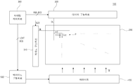
도 2는 본발명의 제 1 실시예에 따른 액정표시장치를 개략적으로 도시한 도면.
도 3은 본발명의 제 1 실시예에 따른 백라이트와 백라이트구동회로를 개략적으로 도시한 도면.
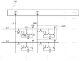
도 4는 본발명의 제 1 실시예에 따른 발광다이오드유닛과 백라이트구동회로의 연결관계을 도시한 회로도.
도 5는 본발명의 제 1 실시예에 따른 발광다이오드의 구동방법을 도시한 회로도.
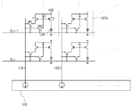
도 6은 본발명의 제 2 실시예에 따른 액정표시장치의 발광다이오드유닛과 백라이트구동회로의 연결관계를 도시한 회로도.
도 7은 본발명의 제 3 실시예에 따른 액정표시장치의 발광다이오드유닛과 백라이트구동회로의 연결관계를 도시한 회로도.
도 8은 본발명의 제 4 실시예에 따른 액정표시장치의 발광다이오드유닛과 백라이트구동회로의 연결관계를 도시한 회로도
도 9는 본발명의 제 5 실시예에 따른 액정표시장치의 발광다이오드유닛과 백라이트구동회로의 연결관계를 도시한 회로도.
도 10은 본발명의 제 6 실시예에 따른 액정표시장치의 발광다이오드유닛과 백라이트구동회로의 연결관계를 도시한 회로도.
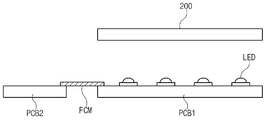
도 11 및 12는 각각, 본발명의 제 7 실시예에 따른 액정표시장치에서 발광다이오드와, 전류미러회로와, 스위칭회로의 배치관계의 일예를 개략적으로 도시한 단면도 및 평면도.
도 13은 본발명의 제 8 실시예에 따른 액정표시장치에서 2개의 제 2 인쇄회로기판이 사용되는 예를 개략적으로 도시한 평면도.
SL : 스캔배선
LDL : 발광데이터배선
LEDU : 발광다이오드유닛
LED : 발광다이오드
T1, T2 : 제 1 및 2 트랜지스터
SW1, SW2 : 제 1 및 2 스위칭소자
C : 스토리지커패시터
Claims (8)
- 영상을 표시하는 액정패널과;
상기 액정패널 하부에 위치하며, 제 1 인쇄회로기판에 실장된 다수의 발광다이오드와;
연성회로부재를 통해 상기 제 1 인쇄회로기판과 연결되는 제 2 인쇄회로기판에 실장되며, 전달배선을 통해 상기 다수의 발광다이오드 각각과 연결되는 전류미러회로와;
상기 전류미러회로에 연결되는 스위칭회로와;
상시 스위칭회로와 연결되며, 스캔신호를 전달하는 스캔배선 및 발광데이터전류를 전달하는 발광데이터배선을 포함하고,
상기 전류미러회로는, 입력된 상기 발광데이터전류에 응답하여 발광전류를 상기 발광다이오드에 출력하는
액정표시장치.
- 제 1 항에 있어서,
상기 전류미러회로는, 상기 발광데이터전류를 입력받는 제 1 트랜지스터와, 상기 발광전류를 상기 전달배선에 출력하는 제 2 트랜지스터를 포함하는
액정표시장치.
- 제 2 항에 있어서,
상기 스위칭회로는 상기 제 2 인쇄회로기판에 실장되며, 상기 스캔신호에 따라 동일하게 스위칭하는 제 1 및 2 스위칭소자를 포함하고,
상기 제 1 스위칭소자는, 상기 발광데이터배선과 상기 제 1 트랜지스터의 드레인단자 사이에 연결되고,
상기 제 2 스위칭소자는, 상기 제 1 트랜지스터의 드레인단자와 게이트단자 사이에 연결되는
액정표시장치.
- 제 2 항에 있어서,
상기 스위칭회로는 상기 제 2 인쇄회로기판에 실장되며, 상기 스캔신호에 따라 동일하게 스위칭하는 제 1 및 2 스위칭소자를 포함하고,
상기 제 1 스위칭소자는, 상기 발광데이터배선과 상기 제 1 트랜지스터의 드레인단자 사이에 연결되고,
상기 제 2 스위칭소자는, 상기 제 1 트랜지스터의 게이트단자와 상기 제 2 트랜지스터의 게이트단자 사이에 연결되는
액정표시장치.
- 제 2 항에 있어서,
상기 스위칭회로는 상기 제 2 인쇄회로기판에 실장되며, 상기 스캔신호에 따라 동일하게 스위칭하는 제 1 및 2 스위칭소자를 포함하고,
상기 제 1 스위칭소자는, 상기 발광데이터배선과 상기 제 1 트랜지스터의 드레인단자 사이에 연결되고,
상기 제 2 스위칭소자는, 상기 발광데이터배선과 상기 제 1 트랜지스터의 게이트단자 사이에 연결되는
액정표시장치.
- 제 2 항에 있어서,
상기 제 2 트랜지스터의 게이트단자와 소스단자 사이에 연결되는 스토리지커패시터를 더욱 포함하는
액정표시장치.
- 제 2 항에 있어서,
상기 제 1 및 2 트랜지스터는, P타입 또는 N타입 트랜지스터인
액정표시장치.
- 제 1 항에 있어서,
상기 제 2 인쇄회로기판에 실장되며 다수의 채널을 갖는 적어도 하나의 구동IC로 구성되는 스캔구동회로와;
상기 제 2 인쇄회로기판에 실장되며 다수의 채널을 갖는 적어도 하나의 구동IC로 구성되는 발광데이터구동회로를 더욱 포함하고,
상기 스캔구동회로의 채널은 상기 스캔배선에 대응되고, 상기 발광데이터구동회로의 채널은 상기 발광데이터배선에 대응되는
액정표시장치.
Priority Applications (3)
| Application Number | Priority Date | Filing Date | Title |
|---|---|---|---|
| KR1020100068895A KR101368738B1 (ko) | 2010-07-16 | 2010-07-16 | 액정표시장치 |
| CN2010105072328A CN102034451A (zh) | 2009-09-30 | 2010-09-29 | 液晶显示装置 |
| US12/895,199 US9123299B2 (en) | 2009-09-30 | 2010-09-30 | Liquid crystal display device including LED unit using current mirror circuit |
Applications Claiming Priority (1)
| Application Number | Priority Date | Filing Date | Title |
|---|---|---|---|
| KR1020100068895A KR101368738B1 (ko) | 2010-07-16 | 2010-07-16 | 액정표시장치 |
Publications (2)
| Publication Number | Publication Date |
|---|---|
| KR20120008185A true KR20120008185A (ko) | 2012-01-30 |
| KR101368738B1 KR101368738B1 (ko) | 2014-03-06 |
Family
ID=45613243
Family Applications (1)
| Application Number | Title | Priority Date | Filing Date |
|---|---|---|---|
| KR1020100068895A Expired - Fee Related KR101368738B1 (ko) | 2009-09-30 | 2010-07-16 | 액정표시장치 |
Country Status (1)
| Country | Link |
|---|---|
| KR (1) | KR101368738B1 (ko) |
Cited By (2)
| Publication number | Priority date | Publication date | Assignee | Title |
|---|---|---|---|---|
| KR20220081249A (ko) * | 2020-12-08 | 2022-06-15 | 삼성전자주식회사 | Led 백라이트 유닛을 포함하는 디스플레이 장치 |
| CN114664257A (zh) * | 2020-12-08 | 2022-06-24 | 三星电子株式会社 | 包括发光二极管背光单元的显示装置 |
Family Cites Families (4)
| Publication number | Priority date | Publication date | Assignee | Title |
|---|---|---|---|---|
| US6859193B1 (en) * | 1999-07-14 | 2005-02-22 | Sony Corporation | Current drive circuit and display device using the same, pixel circuit, and drive method |
| JP4337339B2 (ja) * | 2001-12-18 | 2009-09-30 | サンケン電気株式会社 | 発光ダイオード駆動回路 |
| KR100627311B1 (ko) * | 2004-08-05 | 2006-09-25 | 삼성에스디아이 주식회사 | 액정 표시 장치 |
| KR101157233B1 (ko) * | 2004-10-30 | 2012-06-15 | 엘지디스플레이 주식회사 | 발광 다이오드 백라이트 장치 및 이를 채용한 액정표시장치 |
-
2010
- 2010-07-16 KR KR1020100068895A patent/KR101368738B1/ko not_active Expired - Fee Related
Cited By (3)
| Publication number | Priority date | Publication date | Assignee | Title |
|---|---|---|---|---|
| KR20220081249A (ko) * | 2020-12-08 | 2022-06-15 | 삼성전자주식회사 | Led 백라이트 유닛을 포함하는 디스플레이 장치 |
| CN114664257A (zh) * | 2020-12-08 | 2022-06-24 | 三星电子株式会社 | 包括发光二极管背光单元的显示装置 |
| US12354530B2 (en) | 2020-12-08 | 2025-07-08 | Samsung Electronics Co., Ltd. | Display device including light-emitting diode backlight unit |
Also Published As
| Publication number | Publication date |
|---|---|
| KR101368738B1 (ko) | 2014-03-06 |
Similar Documents
| Publication | Publication Date | Title |
|---|---|---|
| US11514842B2 (en) | LED based display panel including common LED driving circuit and display apparatus including the same | |
| JP4956520B2 (ja) | バックライト装置及びこれを用いた液晶表示装置 | |
| US8830158B2 (en) | Method of local dimming a light source, light source apparatus for performing the method, and display apparatus having the light source apparatus | |
| TWI415097B (zh) | 液晶顯示裝置及其驅動方法 | |
| US8482512B2 (en) | Liquid crystal backlight apparatus | |
| US20120230056A1 (en) | Light source module and electronic device including same | |
| US20100123741A1 (en) | Method of driving a light source, light source apparatus for performing the method and display apparatus having the light source apparatus | |
| US8305332B2 (en) | Backlight unit, liquid crystal display device including the same, and localized dimming method thereof | |
| US9123299B2 (en) | Liquid crystal display device including LED unit using current mirror circuit | |
| KR20110063021A (ko) | 액정표시장치 및 그 구동방법 | |
| KR101423518B1 (ko) | 액정표시장치 | |
| KR101733202B1 (ko) | 발광다이오드 백라이트 유닛 및 그 구동방법 | |
| US20090146942A1 (en) | Backlight apparatus, method of controlling the same and liquid crystal display apparatus having the same | |
| US20080007573A1 (en) | Display device and display system employing same | |
| JP2006323073A (ja) | 液晶表示装置 | |
| US20120013650A1 (en) | Display device | |
| US20090284181A1 (en) | Backlight unit assembly, display device having the same, and method of dimming the display device | |
| KR101760021B1 (ko) | 액정표시장치 및 그 구동방법 | |
| US20120242236A1 (en) | Apparatus and method for led array control | |
| KR101368738B1 (ko) | 액정표시장치 | |
| US8624827B2 (en) | Field sequential display device having longer black insertion period and a plurality of display areas | |
| KR20120061542A (ko) | 발광다이오드 백라이트 및 이를 포함하는 액정표시장치 | |
| KR101869823B1 (ko) | 액정 표시장치와 이의 구동방법 | |
| KR20110070172A (ko) | 액정표시장치 및 그 구동방법 | |
| US20100045710A1 (en) | Backlight apparatus and a liquid crystal display including the same |
Legal Events
| Date | Code | Title | Description |
|---|---|---|---|
| PA0109 | Patent application |
St.27 status event code: A-0-1-A10-A12-nap-PA0109 |
|
| R18-X000 | Changes to party contact information recorded |
St.27 status event code: A-3-3-R10-R18-oth-X000 |
|
| R18-X000 | Changes to party contact information recorded |
St.27 status event code: A-3-3-R10-R18-oth-X000 |
|
| A201 | Request for examination | ||
| PA0201 | Request for examination |
St.27 status event code: A-1-2-D10-D11-exm-PA0201 |
|
| R18-X000 | Changes to party contact information recorded |
St.27 status event code: A-3-3-R10-R18-oth-X000 |
|
| PG1501 | Laying open of application |
St.27 status event code: A-1-1-Q10-Q12-nap-PG1501 |
|
| D13-X000 | Search requested |
St.27 status event code: A-1-2-D10-D13-srh-X000 |
|
| D14-X000 | Search report completed |
St.27 status event code: A-1-2-D10-D14-srh-X000 |
|
| E902 | Notification of reason for refusal | ||
| PE0902 | Notice of grounds for rejection |
St.27 status event code: A-1-2-D10-D21-exm-PE0902 |
|
| P11-X000 | Amendment of application requested |
St.27 status event code: A-2-2-P10-P11-nap-X000 |
|
| P13-X000 | Application amended |
St.27 status event code: A-2-2-P10-P13-nap-X000 |
|
| E902 | Notification of reason for refusal | ||
| PE0902 | Notice of grounds for rejection |
St.27 status event code: A-1-2-D10-D21-exm-PE0902 |
|
| P11-X000 | Amendment of application requested |
St.27 status event code: A-2-2-P10-P11-nap-X000 |
|
| P13-X000 | Application amended |
St.27 status event code: A-2-2-P10-P13-nap-X000 |
|
| E701 | Decision to grant or registration of patent right | ||
| PE0701 | Decision of registration |
St.27 status event code: A-1-2-D10-D22-exm-PE0701 |
|
| GRNT | Written decision to grant | ||
| PR0701 | Registration of establishment |
St.27 status event code: A-2-4-F10-F11-exm-PR0701 |
|
| PR1002 | Payment of registration fee |
St.27 status event code: A-2-2-U10-U11-oth-PR1002 Fee payment year number: 1 |
|
| PG1601 | Publication of registration |
St.27 status event code: A-4-4-Q10-Q13-nap-PG1601 |
|
| FPAY | Annual fee payment |
Payment date: 20170116 Year of fee payment: 4 |
|
| PR1001 | Payment of annual fee |
St.27 status event code: A-4-4-U10-U11-oth-PR1001 Fee payment year number: 4 |
|
| P22-X000 | Classification modified |
St.27 status event code: A-4-4-P10-P22-nap-X000 |
|
| PR1001 | Payment of annual fee |
St.27 status event code: A-4-4-U10-U11-oth-PR1001 Fee payment year number: 5 |
|
| FPAY | Annual fee payment |
Payment date: 20190114 Year of fee payment: 6 |
|
| PR1001 | Payment of annual fee |
St.27 status event code: A-4-4-U10-U11-oth-PR1001 Fee payment year number: 6 |
|
| FPAY | Annual fee payment |
Payment date: 20200116 Year of fee payment: 7 |
|
| PR1001 | Payment of annual fee |
St.27 status event code: A-4-4-U10-U11-oth-PR1001 Fee payment year number: 7 |
|
| PC1903 | Unpaid annual fee |
St.27 status event code: A-4-4-U10-U13-oth-PC1903 Not in force date: 20210225 Payment event data comment text: Termination Category : DEFAULT_OF_REGISTRATION_FEE |
|
| P22-X000 | Classification modified |
St.27 status event code: A-4-4-P10-P22-nap-X000 |
|
| PC1903 | Unpaid annual fee |
St.27 status event code: N-4-6-H10-H13-oth-PC1903 Ip right cessation event data comment text: Termination Category : DEFAULT_OF_REGISTRATION_FEE Not in force date: 20210225 |