KR20120032425A - Image processing apparatus, image processing method, and image processing program - Google Patents
Image processing apparatus, image processing method, and image processing program Download PDFInfo
- Publication number
- KR20120032425A KR20120032425A KR1020110094614A KR20110094614A KR20120032425A KR 20120032425 A KR20120032425 A KR 20120032425A KR 1020110094614 A KR1020110094614 A KR 1020110094614A KR 20110094614 A KR20110094614 A KR 20110094614A KR 20120032425 A KR20120032425 A KR 20120032425A
- Authority
- KR
- South Korea
- Prior art keywords
- mode
- exposure
- charge
- unit
- signal level
- Prior art date
- Legal status (The legal status is an assumption and is not a legal conclusion. Google has not performed a legal analysis and makes no representation as to the accuracy of the status listed.)
- Withdrawn
Links
Images


Classifications
-
- H—ELECTRICITY
- H04—ELECTRIC COMMUNICATION TECHNIQUE
- H04N—PICTORIAL COMMUNICATION, e.g. TELEVISION
- H04N25/00—Circuitry of solid-state image sensors [SSIS]; Control thereof
- H04N25/50—Control of the SSIS exposure
- H04N25/57—Control of the dynamic range
- H04N25/59—Control of the dynamic range by controlling the amount of charge storable in the pixel, e.g. modification of the charge conversion ratio of the floating node capacitance
-
- H—ELECTRICITY
- H04—ELECTRIC COMMUNICATION TECHNIQUE
- H04N—PICTORIAL COMMUNICATION, e.g. TELEVISION
- H04N23/00—Cameras or camera modules comprising electronic image sensors; Control thereof
- H04N23/60—Control of cameras or camera modules
- H04N23/667—Camera operation mode switching, e.g. between still and video, sport and normal or high- and low-resolution modes
-
- H—ELECTRICITY
- H04—ELECTRIC COMMUNICATION TECHNIQUE
- H04N—PICTORIAL COMMUNICATION, e.g. TELEVISION
- H04N23/00—Cameras or camera modules comprising electronic image sensors; Control thereof
- H04N23/70—Circuitry for compensating brightness variation in the scene
- H04N23/72—Combination of two or more compensation controls
-
- H—ELECTRICITY
- H04—ELECTRIC COMMUNICATION TECHNIQUE
- H04N—PICTORIAL COMMUNICATION, e.g. TELEVISION
- H04N23/00—Cameras or camera modules comprising electronic image sensors; Control thereof
- H04N23/70—Circuitry for compensating brightness variation in the scene
- H04N23/73—Circuitry for compensating brightness variation in the scene by influencing the exposure time
-
- H—ELECTRICITY
- H04—ELECTRIC COMMUNICATION TECHNIQUE
- H04N—PICTORIAL COMMUNICATION, e.g. TELEVISION
- H04N23/00—Cameras or camera modules comprising electronic image sensors; Control thereof
- H04N23/70—Circuitry for compensating brightness variation in the scene
- H04N23/76—Circuitry for compensating brightness variation in the scene by influencing the image signals
-
- H—ELECTRICITY
- H04—ELECTRIC COMMUNICATION TECHNIQUE
- H04N—PICTORIAL COMMUNICATION, e.g. TELEVISION
- H04N25/00—Circuitry of solid-state image sensors [SSIS]; Control thereof
- H04N25/50—Control of the SSIS exposure
- H04N25/53—Control of the integration time
-
- H—ELECTRICITY
- H04—ELECTRIC COMMUNICATION TECHNIQUE
- H04N—PICTORIAL COMMUNICATION, e.g. TELEVISION
- H04N25/00—Circuitry of solid-state image sensors [SSIS]; Control thereof
- H04N25/50—Control of the SSIS exposure
- H04N25/57—Control of the dynamic range
- H04N25/58—Control of the dynamic range involving two or more exposures
- H04N25/581—Control of the dynamic range involving two or more exposures acquired simultaneously
- H04N25/583—Control of the dynamic range involving two or more exposures acquired simultaneously with different integration times
-
- H—ELECTRICITY
- H04—ELECTRIC COMMUNICATION TECHNIQUE
- H04N—PICTORIAL COMMUNICATION, e.g. TELEVISION
- H04N25/00—Circuitry of solid-state image sensors [SSIS]; Control thereof
- H04N25/50—Control of the SSIS exposure
- H04N25/57—Control of the dynamic range
- H04N25/58—Control of the dynamic range involving two or more exposures
- H04N25/587—Control of the dynamic range involving two or more exposures acquired sequentially, e.g. using the combination of odd and even image fields
- H04N25/589—Control of the dynamic range involving two or more exposures acquired sequentially, e.g. using the combination of odd and even image fields with different integration times, e.g. short and long exposures
Landscapes
- Engineering & Computer Science (AREA)
- Multimedia (AREA)
- Signal Processing (AREA)
- Transforming Light Signals Into Electric Signals (AREA)
- Solid State Image Pick-Up Elements (AREA)
Abstract
화상 처리 장치는, 광전 변환 소자를 각각 갖는 단위 화소들이 행렬로 2차원적으로 배치된 화소 어레이부, 및 제1 노광 기간에 소정의 축적 전하 이상으로 단위 화소들에 축적된 전하에 기초하는 제1 전하량, 또는 제1 노광 기간을 포함하는 제2 노광 기간에 단위 화소들에 축적된 모든 전하에 기초하는 제2 전하량에 따라 신호 레벨을 결정하는 수문 모드와, 복수회의 노광 기간에 단위 화소들에 축적된 모든 전하에 기초하는 복수의 전하량에 따라 신호 레벨을 결정하는 복수회 노광 모드 중 어느 하나에 의해, 신호 레벨을 결정하는 신호 처리부를 포함한다. The image processing apparatus includes a pixel array unit in which unit pixels each having a photoelectric conversion element are two-dimensionally arranged in a matrix, and a first based on charges accumulated in the unit pixels more than a predetermined accumulated charge in the first exposure period. A hydrologic mode that determines the signal level according to the amount of charge or the second amount of charge based on all the charge accumulated in the unit pixels in the second exposure period including the first exposure period, and accumulates in the unit pixels in the plurality of exposure periods. And a signal processing section for determining the signal level by any one of the plurality of exposure modes for determining the signal level in accordance with the plurality of charge amounts based on all the charges.
Description
본 발명은 화상 처리 장치, 화상 처리 방법, 및 화상 처리 프로그램에 관한 것이다. The present invention relates to an image processing apparatus, an image processing method, and an image processing program.
CMOS 이미지 센서를 갖는 촬상 장치, 예를 들어, 비디오 카메라나 디지털 스틸 카메라는, 옥내, 옥외, 낮 동안, 그리고 야간 동안 등과 같은 다양한 환경에서 촬영하기 위해 사용된다. 수광되는 광의 변화에 따라, CMOS 이미지 센서에 있어서의 전하 축적 기간을 제어하는 전자 셔터는 노광 시간을 조정함으로써 감도를 최적값으로 설정한다. Imaging devices with CMOS image sensors, such as video cameras or digital still cameras, are used to shoot in various environments, such as indoors, outdoors, during the day, during the night, and the like. In accordance with the change in the received light, the electronic shutter which controls the charge accumulation period in the CMOS image sensor sets the sensitivity to an optimum value by adjusting the exposure time.
CMOS 이미지 센서를 사용하여 다이내믹 레인지를 확대하기 위해서는, 전자 셔터를 고속으로 릴리즈(release)함으로써 노광 시간을 조정하는 방법, 고속으로 복수의 프레임을 촬영해서 촬상 결과를 중첩하는 방법, 및 기타 다른 방법들이 있다. In order to expand the dynamic range using a CMOS image sensor, a method of adjusting the exposure time by releasing the electronic shutter at high speed, taking a plurality of frames at high speed and superimposing the imaging results, and other methods have.
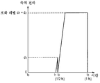
일본 공개 특허 공보 제2008-99158호에서는, 저 조도에서 통상의 포화 레벨을 좁히지 않고, 높은 신호-대-노이즈 비율로 선형적인 신호를 취득할 수 있고, 통상의 포화 레벨 이상인 레벨의 입사광에 대하여도 선형적인 영역에서 만족할 만한 신호-대-노이즈 비율을 실현하면서, 다이내믹 레인지를 확대할 수 있는 기술이 개시되어 있다. 이 방법에서는, 예를 들어, 도 9에 도시된 바와 같이, t4와 t5 사이의 시간을 1 프레임의 노광 시간 t0 내지 t6의 1/16로 설정한다. 그리고, 시간 t4에 축적 전하 dM 이상의 전하를 리셋하고, 다시 t4와 t5 사이에 노광을 행하고, 시간 t5에 축적 전하 dM 이상의 전하를 리셋한다. t4와 t5 사이에 노광된 전하량 d3 - dM과, 1 프레임의 노광 시간(t0 내지 t6)에 노광된 전하량 d4에 기초하여, 1 프레임의 노광에 의해 얻어지는 전하량을 산출한다. 이하, 이 방식을 수문 방식(water gate method)이라고 한다. In Japanese Laid-Open Patent Publication No. 2008-99158, a linear signal can be obtained at a high signal-to-noise ratio without narrowing the normal saturation level at low illuminance, and also for incident light at a level above the normal saturation level. A technique is disclosed that can extend the dynamic range while realizing satisfactory signal-to-noise ratios in the linear domain. In this method, for example, as shown in Fig. 9, the time between t 4 and t 5 is set to 1/16 of the exposure time t 0 to t 6 of one frame. Then, at a time t 4 , the charge of the accumulated charge d M or more is reset, and exposure is performed again between t 4 and t 5 , and at a time t 5 , the charge of the accumulated charge d M or more is reset. t the amount of charge exposure between 4 and t 5 d 3 - and d based on the M and exposed to an exposure time (t 0 to t 6) of one frame amount of charge d 4, and calculates the amount of charge obtained by the exposure of one frame . Hereinafter, this method is called a water gate method.
전술한 수문 방식은, 어두운 촬영 신(scene)에서는 긴 노광 시간, 예를 들어, 도 9의 t0 내지 t6의 노광 시간을 사용하기 때문에, 암부의 신호-대-노이즈 비율이 향상되는 와이드 다이내믹 레인지 방식(wide dynamic range method)이다. 그러나, 이 방식에 의하면, 도 9의 예에 도시된 t4 내지 t5의 노광 시간과, t0 내지 t6의 1 프레임의 노광 시간 간의 비율에 기초하여, 1 프레임의 본래의 축적 전하량을 추정하기 때문에, 노광 시간을 자유롭게 변경할 수 없다. 그 결과, 이 방식은, 밝은 촬영 신에서는 촬상 장치의 아이리스(iris)(조리개)의 개구를 좁힘으로써 대응한다. Since the above-described hydrological method uses a long exposure time in a dark photographic scene, for example, an exposure time of t 0 to t 6 in FIG. 9, wide dynamics in which the signal-to-noise ratio of the dark part is improved. It is a wide dynamic range method. According to this system, however, the original accumulated charge amount of one frame is estimated based on the ratio between the exposure time of t 4 to t 5 and the exposure time of one frame of t 0 to t 6 shown in the example of FIG. 9. Therefore, the exposure time cannot be changed freely. As a result, this system responds by narrowing the opening of the iris (aperture) of the imaging device in a bright shooting scene.
그러나, 아이리스를 이용하는 노광 제어는 밝은 촬영 신에서 아이리스의 개구를 작게 한다. 그 결과, 광의 회절에 기인하여 화상 전체에 흐려짐(blurring)이 발생하여(소위, 회절 현상), 초점을 맞추기 어렵게 한다. However, exposure control using the iris makes the opening of the iris small in bright shooting scene. As a result, blurring occurs throughout the image due to diffraction of light (so-called diffraction phenomenon), making it difficult to focus.
밝은 촬영 신에서 아이리스를 이용하는 노광 제어를 행하지 않고, 어두운 촬영 신에서 신호-대-노이즈 비율을 향상시킨 와이드 다이내믹 레인지를 실현할 수 있는, 신규하고 개량된 화상 처리 장치, 화상 처리 방법, 및 화상 처리 프로그램을 제공하는 것이 바람직하다. A novel and improved image processing apparatus, image processing method, and image processing program capable of realizing a wide dynamic range with improved signal-to-noise ratio in a dark imaging scene without performing exposure control using an iris in a bright imaging scene. It is desirable to provide.
본 발명의 실시예에 따르면, 광을 전하로 변환하는 광전 변환 소자를 각각 갖는 단위 화소들이 행렬로 2차원적으로 배치된 화소 어레이부, 및 제1 노광 기간에 미리 결정된 축적 전하 이상으로 상기 단위 화소들에 축적된 전하에 기초하는 제1 전하량, 또는 상기 제1 노광 기간을 포함하는 제2 노광 기간에 상기 단위 화소들에 축적된 모든 전하에 기초하는 제2 전하량에 따라 신호 레벨을 결정하는 모드인 수문 모드와, 복수회의 노광 기간에 상기 단위 화소들에 축적된 모든 전하에 기초하는 복수의 전하량에 따라 신호 레벨을 결정하는 모드인 복수회 노광 모드 중 어느 하나를 사용하여, 상기 신호 레벨을 결정하는 신호 처리부를 포함하는, 화상 처리 장치가 제공된다. According to an embodiment of the present invention, a pixel array unit in which unit pixels each having photoelectric conversion elements for converting light into charges are two-dimensionally arranged in a matrix, and the unit pixels are larger than or equal to a predetermined accumulated charge in a first exposure period. Is a mode for determining a signal level according to a first charge amount based on charges accumulated in the field or a second charge amount based on all charges accumulated in the unit pixels in a second exposure period including the first exposure period. The signal level is determined using any one of a hydrological mode and a plurality of exposure modes which are modes for determining a signal level according to a plurality of charge amounts based on all charges accumulated in the unit pixels in a plurality of exposure periods. An image processing apparatus including a signal processing unit is provided.
상기 신호 처리부는, 상기 전하에 기초하는 검출값에 따라 상기 신호 레벨을 조정하는 게인을 결정할 수 있고, 상기 게인에 기초하여 모드를 상기 수문 모드와 상기 복수회 노광 모드 중 어느 하나로 전환할 수 있다.The signal processing unit may determine a gain for adjusting the signal level according to a detection value based on the charge, and switch the mode to either the hydrological mode or the multiple exposure mode based on the gain.
상기 모드가 상기 수문 모드일 때, 상기 신호 처리부는, 상기 게인이 0이 될 경우에 상기 모드를 상기 복수회 노광 모드로 전환할 수 있다. 또한, 상기 모드가 상기 복수회 노광 모드일 때, 상기 신호 처리부는, 상기 게인이 미리 설정된 히스테리시스 이상이 될 경우에 상기 모드를 상기 수문 모드로 전환할 수 있다. When the mode is the hydrologic mode, the signal processor may switch the mode to the plurality of exposure modes when the gain becomes zero. In addition, when the mode is the plurality of exposure modes, the signal processor may switch the mode to the hydrological mode when the gain is equal to or greater than a preset hysteresis.
또한, 본 발명의 다른 실시예에 따르면, 광전 변환 소자를 각각 갖는 단위 화소들이 행렬로 2차원적으로 배치된 화소 어레이부를 이용하여 광을 전하로 변환하는 단계, 및 신호 처리부가, 제1 노광 기간에 미리 결정된 축적 전하 이상으로 상기 단위 화소들에 축적된 전하에 기초하는 제1 전하량, 또는 상기 제1 노광 기간을 포함하는 제2 노광 기간에 상기 단위 화소들에 축적된 모든 전하에 기초하는 제2 전하량에 따라 신호 레벨을 결정하는 모드인 수문 모드와, 복수회의 노광 기간에 상기 단위 화소들에 축적된 모든 전하에 기초하는 복수의 전하량에 따라 신호 레벨을 결정하는 모드인 복수회 노광 모드 중 어느 하나를 사용하여, 상기 신호 레벨을 결정하는 단계를 포함하는, 화상 처리 방법이 제공된다. Further, according to another embodiment of the present invention, the step of converting light into electric charge by using a pixel array unit in which the unit pixels each having a photoelectric conversion element is arranged two-dimensionally in a matrix, and the signal processing unit, the first exposure period A first charge amount based on charges accumulated in the unit pixels above a predetermined accumulated charge, or a second based on all charges accumulated in the unit pixels in a second exposure period including the first exposure period. Any one of a hydrological mode that is a mode for determining a signal level in accordance with an amount of charge and a plurality of exposure modes that are a mode for determining a signal level in accordance with a plurality of charge amounts based on all charges accumulated in the unit pixels in a plurality of exposure periods; An image processing method is provided, comprising determining the signal level.
또한, 본 발명의 또 다른 실시예에 따르면, 광전 변환 소자를 각각 갖는 단위 화소들이 행렬로 2차원적으로 배치된 화소 어레이부를 이용하여 광을 전하로 변환하는 단계, 및 신호 처리부가, 제1 노광 기간에 미리 결정된 축적 전하 이상으로 상기 단위 화소들에 축적된 전하에 기초하는 제1 전하량, 또는 상기 제1 노광 기간을 포함하는 제2 노광 기간에 상기 단위 화소들에 축적된 모든 전하에 기초하는 제2 전하량에 따라 신호 레벨을 결정하는 모드인 수문 모드와, 복수회의 노광 기간에 상기 단위 화소들에 축적된 모든 전하에 기초하는 복수의 전하량에 따라 신호 레벨을 결정하는 모드인 복수회 노광 모드 중 어느 하나를 사용하여, 상기 신호 레벨을 결정하는 단계를 포함하는 처리를, 컴퓨터에 실행시키기 위한 프로그램이 제공된다. Further, according to another embodiment of the present invention, the step of converting light into electric charge by using a pixel array unit in which the unit pixels each having a photoelectric conversion element is two-dimensionally arranged in a matrix, and the signal processing unit, the first exposure A first charge amount based on charges accumulated in the unit pixels above a predetermined accumulated charge in a period, or a first charge based on all charges accumulated in the unit pixels in a second exposure period including the first exposure period. The hydrological mode, which is a mode for determining the signal level in accordance with the amount of charges, and the multiple exposure mode, in which the signal level is determined in accordance with the plurality of charges based on all the charges accumulated in the unit pixels in the plurality of exposure periods. Using one, a program is provided for causing a computer to execute a process comprising determining the signal level.
전술한 바와 같이, 본 발명의 실시예에 따르면, 밝은 촬영 신에서 아이리스를 이용한 노광 제어를 행하지 않고, 어두운 촬영 신에서 신호-대-노이즈 비율을 향상시킨 와이드 다이내믹 레인지를 실현할 수 있다. As described above, according to the embodiment of the present invention, it is possible to realize a wide dynamic range in which the signal-to-noise ratio is improved in a dark imaging scene without performing exposure control using an iris in a bright imaging scene.
도 1은 본 발명의 실시예에 따른 CMOS 이미지 센서의 구성 예를 도시하는 시스템 구성도이다.
도 2는 단위 화소의 구성의 예를 도시하는 회로도이다.
도 3은 드라이버 회로의 구성의 예를 도시하는 회로도이다.
도 4는 통상의 판독의 경우의 동작을 설명하기 위한 타이밍도이다.
도 5는 신호-대-노이즈 비율을 향상시키고 다이내믹 레인지를 확대하기 위한 동작을 설명하기 위한 타이밍도이다.
도 6은 전송 트랜지스터의 제어 전극에 복수의 전압을 선택적으로 공급할 경우의 화소에 있어서의 전위의 예를 도시하는 전위도이다.
도 7은 복수회 노광 모드에서의 축적 전하와 시간 간의 관계를 도시하는 그래프이다.
도 8은 복수회 노광 모드에서의 축적 전하와 시간 간의 관계를 도시하는 그래프로서, 도 7의 휘도보다 휘도가 낮은 경우를 도시하는 그래프이다.
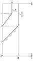
도 9는 수문 모드에서의 축적 전하와 시간 간의 관계를 도시하는 그래프이다.
도 10은 수문 모드에서의 축적 전하와 시간 간의 관계를 도시하는 그래프로서, 도 9의 휘도보다 휘도가 낮은 경우를 도시하는 그래프이다.
도 11은 수문 모드에서의 축적 전하와 시간 간의 관계를 도시하는 그래프로서, 도 10의 휘도보다 휘도가 낮은 경우를 도시하는 그래프이다.
도 12는 수문 모드에서의 축적 전하와 시간 간의 관계를 도시하는 그래프로서, 도 11의 휘도보다 휘도가 낮은 경우를 도시하는 그래프이다.
도 13은 게인과 휘도 간의 관계, 및 아이리스와 휘도 간의 관계를 도시하는 그래프로서, 종래 기술의 노광 제어의 천이를 도시하는 그래프이다.
도 14는 게인과 휘도 간의 관계, 및 아이리스와 휘도 간의 관계를 도시하는 그래프로서, 본 발명의 실시예의 노광 제어의 천이를 도시하는 그래프이다.
도 15는 게인과 휘도 간의 관계, 및 아이리스와 휘도 간의 관계를 도시하는 그래프로서, 본 발명의 실시예의 노광 제어의 천이를 도시하며, 변경예를 도시하는 그래프이다.
도 16은 본 발명의 실시예의 수문 모드와 복수회 노광 모드 간의 전환 동작을 도시하는 흐름도이다.
도 17은 수문 모드의 축적 전하량의 산출 동작을 도시하는 흐름도이다.
도 18은 본 발명의 실시예에 따른 촬상 장치의 구성의 예를 도시하는 블록도이다. 1 is a system configuration diagram showing a configuration example of a CMOS image sensor according to an embodiment of the present invention.
2 is a circuit diagram illustrating an example of a configuration of a unit pixel.
3 is a circuit diagram illustrating an example of a configuration of a driver circuit.
4 is a timing diagram for explaining the operation in the case of normal reading.
5 is a timing diagram for explaining an operation for improving the signal-to-noise ratio and expanding the dynamic range.
6 is a potential diagram showing an example of a potential in a pixel when a plurality of voltages are selectively supplied to a control electrode of a transfer transistor.
7 is a graph showing a relationship between accumulated charge and time in a plurality of exposure modes.
FIG. 8 is a graph showing a relationship between accumulated charge and time in a plurality of exposure modes, and is a graph showing a case where luminance is lower than that of FIG.
9 is a graph showing the relationship between accumulated charge and time in the hydrologic mode.
FIG. 10 is a graph showing the relationship between the accumulated charge and the time in the hydrological mode, and is a graph showing the case where the luminance is lower than the luminance of FIG.
FIG. 11 is a graph showing the relationship between the accumulated charge and the time in the hydrological mode, showing a case where the luminance is lower than that of FIG.
FIG. 12 is a graph showing the relationship between the accumulated charge and the time in the hydrological mode, and is a graph showing the case where the luminance is lower than the luminance of FIG.
Fig. 13 is a graph showing the relationship between the gain and the luminance and the relationship between the iris and the luminance, which is a graph showing the transition of exposure control in the prior art.
Fig. 14 is a graph showing the relationship between the gain and the luminance and the relationship between the iris and the luminance, which is a graph showing the transition of exposure control in the embodiment of the present invention.
Fig. 15 is a graph showing the relationship between the gain and the luminance and the relationship between the iris and the luminance, showing the transition of exposure control in the embodiment of the present invention, and showing a modification.
16 is a flowchart showing a switching operation between the hydrological mode and the multiple times exposure mode in the embodiment of the present invention.
17 is a flowchart showing an operation of calculating the accumulated charge amount in the hydrologic mode.
18 is a block diagram illustrating an example of a configuration of an imaging device according to an embodiment of the present invention.
이하, 첨부 도면을 참조하여, 본 발명의 바람직한 실시예에 대해서 상세하게 설명한다. 또한, 본 명세서 및 도면에 있어서, 실질적으로 동일한 기능을 갖는 구성 요소에 대해서는 동일한 참조 부호를 병기하고, 중복적인 설명을 생략한다는 것을 유의한다. Hereinafter, with reference to the accompanying drawings, a preferred embodiment of the present invention will be described in detail. In addition, in this specification and drawing, it is noted that the same referential mark is attached | subjected about the component which has a substantially same function, and redundant description is abbreviate | omitted.
또한, 설명은 다음의 순서로 행한다. In addition, description is given in the following procedure.
1. 실시예의 구성1. Configuration of Example
2. 실시예의 동작
2. Operation of the embodiment
1. 실시예의 구성1. Configuration of Example
도 1은 본 발명의 실시예에 따른 고체 촬상 장치, 예를 들어, CMOS 이미지 센서의 구성예를 도시하는 시스템 구성도이다. 1 is a system configuration diagram showing a configuration example of a solid-state imaging device according to an embodiment of the present invention, for example, a CMOS image sensor.
도 1에 도시된 바와 같이, 본 실시예에 따른 CMOS 이미지 센서(10)는, 광전 변환 소자를 각각 포함하는 단위 화소들(이하, 간단히 화소들이라고도 칭함)(20)이 행렬로 2차원적으로 배치되어 있는 화소 어레이부(11)를 포함하고, 또한, 화소 어레이부(11)의 주변 회로들로서, 행 선택 회로(12), 선행(advance) 선택 회로(13), 논리 회로(14), 드라이버 회로(15), 컨트롤러 유닛(16), 전압 공급 회로(17), 컬럼 회로(18), 및 수평 주사 회로(19)를 포함한다. As shown in FIG. 1, in the
화소 어레이부(11)에는 단위 화소들(20)의 행렬 배열에 대하여, 각각의 열(컬럼)에 대해 수직 신호선(111)이 배치되고, 각각의 행에 대해 구동 제어선들, 예를 들어, 전송 제어선(112), 리셋 제어선(113), 및 선택 제어선(114)이 배치된다.In the
<화소 회로><Pixel circuit>
도 2에 단위 화소(20)의 구성의 예가 도시된다. 본 회로 예에 따른 단위 화소(20)는 광전 변환 소자, 예를 들어, 포토다이오드(21) 외에도, 예를 들어, 전송 트랜지스터(22), 리셋 트랜지스터(23), 증폭 트랜지스터(24), 및 선택 트랜지스터(25)의 4개의 트랜지스터를 포함하는 화소 구성, 즉, 본 발명의 실시예에 따른 전송 게이트에 상당하는 전송 트랜지스터(22)를 갖는 파괴적 판독의 화소 구성을 갖는다. 여기에서, 트랜지스터들(22 내지 25)로서, 예를 들어, NMOS 트랜지스터가 사용된다. 2 shows an example of the configuration of the
전송 트랜지스터(22)는 포토다이오드(21)의 캐소드 전극과 전하 전압 변환부인 FD(플로팅 디퓨전(floating diffusion))부(26) 사이에 접속되고, 포토다이오드(21)로 광전 변환되어 거기에 축적된 신호 전하(여기서는, 전자들)를, 게이트 전극(제어 전극)에 전송 펄스 TRG가 제공됨으로써, FD부(26)에 전송한다. The
리셋 트랜지스터(23)의 드레인 전극은 화소 전원 VDD에 접속되고, 리셋 트랜지스터(23)의 소스 전극은 FD부(26)에 접속된다. 리셋 트랜지스터(23)는, 포토다이오드(21)로부터 FD부(26)에의 신호 전하의 전송 전에, 게이트 전극에 리셋 펄스 RST가 제공됨으로써, FD부(26)의 전위(electric potential)를 소정 전위로 리셋한다. The drain electrode of the
증폭 트랜지스터(24)의 게이트 전극은 FD부(26)에 접속되고, 증폭 트랜지스터(24)의 드레인 전극은 화소 전원 VDD에 접속된다. 증폭 트랜지스터(24)는 FD부(26)의 전위, 즉, 리셋 트랜지스터(23)에 의해 리셋이 행해진 후 얻어진 전위를 리셋 레벨로서 출력하고, 또한 FD부(26)의 전위, 즉, 전송 트랜지스터(22)에 의해 신호 전하의 전송이 행해진 후 얻어진 전위를 신호 레벨로서 출력한다. The gate electrode of the amplifying
예를 들어, 선택 트랜지스터(25)의 드레인 전극은 증폭 트랜지스터(24)의 소스 전극에 접속되고, 선택 트랜지스터(25)의 소스 전극은 수직 신호선(111)에 접속된다. 선택 트랜지스터(25)는 게이트 전극에 선택 펄스 SEL이 제공됨으로써 온(ON) 상태로 되어, 화소(20)의 상태를 선택 상태로 변경하고, 증폭 트랜지스터(24)로부터 출력되는 신호를 수직 신호선(111)에 출력한다. For example, the drain electrode of the
또한, 선택 트랜지스터(25)가 화소 전원 VDD와 증폭 트랜지스터(24)의 드레인 전극 사이에 접속되는 구성을 채택할 수도 있다. 또한, 화소 회로의 구성은 전술한 4 트랜지스터의 구성에 한정되지 않는다. 화소 회로는, 선택 트랜지스터(25)를 생략하고, 증폭 트랜지스터(24)를 선택 트랜지스터(25)로서 겸용하는 3 트랜지스터 구성이나, 또는 증폭 트랜지스터(24)를 복수의 단위 화소 간에 공유하는 구성을 채택할 수 있다. Further, a configuration in which the
<행 선택 회로><Row selection circuit>
행 선택 회로(12)는 본 발명의 실시예에 따른 제1 구동 유닛에 상당하고, 시프트 레지스터 또는 어드레스 디코더 등으로 형성된다. 행 선택 회로(12)는 컨트롤러 유닛(16)의 제어 하에, 전송 펄스 TRG, 리셋 펄스 RST, 및 선택 펄스 SEL 등의 화소 구동 펄스를 적절히 발생함으로써, 화소 어레이부(11)의 화소들(20)을 각각의 전자 셔터 행과 각각의 판독 행에 대해서 행 단위로 수직 방향(상하 방향)으로 주사하면서 선택하고, 전자 셔터 행에 대하여는 그 행의 화소들(20)의 신호를 스위핑(sweeping)하기 위한 전자 셔터 동작을 행하고, 판독 행에 대하여는 그 행의 화소들(20)의 신호를 판독하기 위한 판독 동작을 행한다. The row
도면에 도시되지는 않았지만, 행 선택 회로(12)는, 화소들(20)을 행 단위로 순서대로 선택 주사하면서, 판독 행의 각 화소(20)의 신호를 판독하는 판독 동작을 행하기 위한 판독 주사계와, 판독 주사계에 의해 행해지는 판독 주사보다 셔터 속도에 대응한 시간만큼 선행해서 동일한 행(전자 셔터 행)에 대하여 전자 셔터 동작을 행하기 위한 전자 셔터 주사계를 갖는다. Although not shown in the drawing, the
전자 셔터 주사계에 의해 행해지는 전자 셔터 동작에 의해 포토다이오드(21)의 불필요한 전하가 리셋되는 시간으로부터, 판독 주사계에 의해 행해지는 판독 동작에 의해 화소(20)의 신호가 판독되는 시간까지의 기간이, 화소(20)에 있어서의 신호 전하의 축적 기간(제1 노광 시간)이 된다. 즉, 전자 셔터 동작이란, 포토다이오드(21)에 축적된 신호 전하의 리셋(스위핑)을 행하고, 리셋 후에 새롭게 신호 전하의 축적을 개시하는 동작이다. From the time when the unnecessary charge of the
<선행 선택 회로> <Lead selection circuit>
선행 선택 회로(13)는 본 발명의 실시예에 따른 제2 구동 유닛에 상당한다. 선행 선택 회로(13)는 복수의 행 선택 회로, 예를 들어, 2개의 행 선택 회로(13A, 13B)로 형성되고, 행 선택 회로(12)에 의해 선택 주사가 행해지는 판독 행에 선행해서 등 간격으로 복수의 행(본 예에서는, 2개의 행)을 선택 주사한다. The preceding
행 선택 회로(13A, 13B)는 시프트 레지스터 또는 어드레스 디코더 등으로 각각 형성된다. 행 선택 회로(13A, 13B)는 컨트롤러 유닛(16)의 제어 하에, 행 선택 회로(12)에 의해 행해지는 선택 주사에 동기하여 전송 펄스 TRG를 적절히 발생함으로써, 행 선택 회로(12)에 의해 선택 주사가 행해지는 판독 행에 선행해서 등간격으로 2개의 행을 선택 주사한다. 선택 주사에서는, 전송 펄스 TRG에 기초하여, 포토다이오드(21)에 축적된 신호 전하를 FD부(26)에 전송하는 동작이 행해진다. 이 동작의 상세한 사항에 대해서는 후술한다. The row
<논리 회로> <Logic Circuit>
논리 회로(14)는 컨트롤러 유닛(16)의 제어 하에, 행 선택 회로(12), 및 선행 선택 회로(13)의 2개의 행 선택 회로(13A, 13B)로부터 행 선택을 위해서 출력되는 전송 펄스 TRG, 리셋 펄스 RST, 및 선택 펄스 SEL을 드라이버 회로(15)를 통해서 화소 어레이부(11)의 전송 제어선(112), 리셋 제어선(113), 및 선택 제어선(114)에 공급하고, 후술하는 바와 같이, 전송 펄스 TRG의 전압값을 선택하기 위한 신호를 드라이버 회로(15)에 제공한다. The
<드라이버 회로> <Driver circuit>
드라이버 회로(15)는 행 선택 회로(12)에 의해 행해지는 선택 주사에 동기하여, 화소(20)의 트랜지스터들(22, 23, 25)을 턴 ON/OFF하기 위한 전압의 전송 펄스 TRG, 리셋 펄스 RST, 및 선택 펄스 SEL을 화소(20)에 공급하고, 행 선택 회로(13A, 13B)에 의해 행해지는 선택 주사에 동기하여, 화소(20)의 트랜지스터들(22, 23, 25)을 턴 ON/OFF하기 위한 전압의 중간 전압(이하, 중간 전압이라고 칭함)의 전송 펄스 TRG를 화소(20)에 공급한다. 즉, 드라이버 회로(15)는 본 발명의 실시예에 따른 제1 내지 제3 공급 전압 제어 유닛으로서의 기능을 한다. The
도 3은 드라이버 회로(15)의 구성의 예를 도시하는 회로도이다. 여기에서, 어떤 행에 대응한 드라이버 회로(15)의 전송 펄스 TRG에 대한 단위 회로의 구성이 도시된다. 전송 펄스 TRG에 대한 단위 회로들이, 리셋 펄스 RST 및 선택 펄스 SEL에 대한 단위 회로들과 함께, 화소 어레이부(11)의 행 개수만큼 배치됨으로써 드라이버 회로(15)가 구성된다. 3 is a circuit diagram illustrating an example of the configuration of the
도 3에 도시된 바와 같이, 본 예에 따른 드라이버 회로(단위 회로)(15)는, 전압 공급 회로(17)로부터 공급되는, 예를 들어, 3개의 전압 Vtrg1, Vtrg2, 및 Vtrg3에 대응한 3개의 회로 블록(131 내지 133)과, 2 입력의 NOR 회로(134)를 포함하는 회로 구성을 갖는다. As shown in FIG. 3, the driver circuit (unit circuit) 15 according to the present example is supplied to, for example, three voltages V trg1 , V trg2 , and V trg3 supplied from the
3개의 전압 Vtrg1, Vtrg2, 및 Vtrg3 중에서, 전압 Vtrg1과 Vtrg3은 화소(20)의 트랜지스터들(22, 23, 25)을 턴 ON/OFF하기 위한 전압으로서 기능하고, 전압 Vtrg2는 전술한 중간 전압으로서 기능한다. Among the three voltages V trg1 , V trg2 , and V trg3 , the voltages V trg1 and V trg3 function as voltages for turning ON / OFF the
드라이버 회로(15)에는 행 선택 회로(12) 및 행 선택 회로(13A, 13B)로부터 어드레스 신호 ADR이 제공된다. 또한, 컨트롤러 유닛(16)의 제어 하에, 행 선택이 행해지는 시간에 논리 회로(14)로부터 타이밍 신호 PTRG1이 드라이버 회로(15)에 제공되고, 중간 전압이 인가되는 시간에 타이밍 신호 PTRG2가 드라이버 회로(15)에 제공된다. The
회로 블록(131)은, 어드레스 신호 ADR과 타이밍 신호 PTRG1을 2 입력으로서 이용하는 NAND 회로(1311)와, P 채널 구동 트랜지스터(1312)로 형성된다. 회로 블록(131)은 전압 Vtrg1을 선택해서 전송 트랜지스터(22)의 게이트 전극에 전압 Vtrg1을 공급한다. The
회로 블록(132)은, 어드레스 신호 ADR과 타이밍 신호 PTRG2를 2 입력으로서 이용하는 AND 회로(1321)와, N 채널 구동 트랜지스터(1322)로 형성된다. 회로 블록(132)은 중간 전압인 전압 Vtrg2를 선택해서 전송 트랜지스터(22)의 게이트 전극에 전압 Vtrg2를 공급한다. The
회로 블록(133)은, 어드레스 신호 ADR을 일(네가티브) 입력으로서 이용하고 NOR 회로(134)의 출력 신호를 타 입력으로서 이용하는 OR 회로(1331)와, N 채널 구동 트랜지스터(1332)로 형성된다. 회로 블록(133)은 전압 Vtrg3을 선택해서 전송 트랜지스터(22)의 게이트 전극에 전압 Vtrg3을 공급한다. The
즉, 회로 블록(133)은, 전송 트랜지스터(22)를 턴 OFF하기 위한 전압으로서, 예를 들어, 접지 전압 또는 접지 전압보다 낮은 전압(예를 들어, -1.0V)을 공급하기 위해서, 회로 블록(133)이 NOR 회로(134)의 작용에 의해 다른 회로 블록(131, 132)과는 배타적으로 동작하는 회로 구성을 갖는다. That is, the
<컬럼 회로><Column circuit>
컬럼 회로(18)는 화소 어레이부(11)의, 예를 들어, 각각의 화소 열에 대해 배치된 단위 회로들의 그룹으로 형성되며, 즉, 단위 회로들과 화소 열들이 1 대 1의 관계를 갖도록 배치된다. 컬럼 회로(18)는 행 선택 회로(12) 및 행 선택 회로(13A, 13B)에 의해 선택된 판독 행의 화소들(20)로부터 수직 신호선(111)을 통해서 출력되는 신호에 대하여 소정의 신호 처리를 행하고, 신호 처리된 화소 신호를 일시적으로 보유한다. The
컬럼 회로(18)로서는, 수직 신호선(111)을 통해서 출력되는 신호를 샘플링하여 보유하는 샘플 앤드 홀드(sample and hold) 회로로 형성되는 회로 구성을 갖는 컬럼 회로이거나, 또는 샘플 앤드 홀드 회로를 포함하고 상관 이중 샘플링(correlated double sampling(CDS)) 처리에 의해 리셋 노이즈나 증폭 트랜지스터(24)의 임계값 변동 등과 같은 화소 고유의 고정 패턴 노이즈를 제거하는 노이즈 제거 회로로 형성되는 회로 구성을 갖는 컬럼 회로가 사용된다. The
그러나, 전술한 컬럼 회로(18)의 구성은 단지 예일 뿐이고, 본 발명은 이것에 한정되지 않는다. 예를 들어, 컬럼 회로(18)가 아날로그/디지털(A/D) 변환 기능을 갖고, 신호 레벨을 디지털 신호로서 출력하는 구성도 채택될 수 있다. However, the configuration of the above-described
<수평 주사 회로><Horizontal Scanning Circuit>
수평 주사 회로(19)는 시프트 레지스터 또는 어드레스 디코더 등으로 형성된다. 수평 주사 회로(19)는 화소 어레이부(11)의 각각의 화소 열에 대해 컬럼 회로(18)의 단위 회로들을 순차적으로 수평 주사하면서, 컬럼 회로(18)의 단위 회로들에 일시적으로 보유되어 있는 신호, 즉 화소들의 신호를 순차 출력한다. The
다음으로, 전술한 구성의 본 실시예에 따른 CMOS 이미지 센서(10)의 동작에 대해 도 4에 도시된 타이밍도를 사용하여 설명한다. Next, the operation of the
도 2에 도시된 화소 회로 구성을 각각 갖는 단위 화소들(20)이 행렬로 배치되어 형성된 CMOS 이미지 센서(10)에서는, 일반적으로, 도 4에 도시된 바와 같이, 기간 T1에 포토다이오드(21) 및 FD부(26)를 소정 전위로 리셋하고, 기간 T2에 수광된 광을 전자들로 광전 변환하고 그 전자들을 포토다이오드(21)에 축적한다. 또한, 기간 T2의 후반 부분의 기간 T4에 FD부(26)를 리셋하고, 이때의 FD부(26)의 전위를 리셋 레벨로서 판독하고, 그런 다음 기간 T3에 포토다이오드(21)에 축적된 전자들을 FD부(26)에 전송하고, 이때의 FD부(26)의 전위를 기간 T5에 신호 레벨로서 판독한다. In the
이 통상의 판독 동작과는 달리, 본 발명의 실시예에서는, 신호-대-노이즈 비율을 향상시키고 다이내믹 레인지를 확대하기 위해 다음의 구동이 행해진다. 광전 변환에 의해 전자들을 축적하는 축적 기간(제1 노광 시간)에 있어서, 전송 트랜지스터(22)의 게이트 전극에 제1 제어 전압을 공급하고, 제1 제어 전압과는 다른 전압값의 제2 제어 전압을 전송 트랜지스터(22)의 게이트 전극에 1회 또는 복수회 공급한다. 제2 제어 전압들 중 1개 또는 복수개의 전압의 공급에 선행하여, 그 1개의 제2 제어 전압 또는 복수개의 제2 제어 전압 각각과 같은 전압값의 제3 제어 전압을 전송 트랜지스터(22)의 게이트 전극에 1회 또는 복수회 공급한다. 제1 제어 전압이 공급될 때 전송 트랜지스터(22)에 의해 FD부(26)에 전송되는 신호 전하를 판독하고, 제2 제어 전압들이 순차 공급될 때 전송 트랜지스터(22)에 의해 FD부(26)에 전송되는 신호 전하를 1회 이상 판독한다. Unlike this normal read operation, in the embodiment of the present invention, the following drive is performed to improve the signal-to-noise ratio and to expand the dynamic range. In an accumulation period (first exposure time) in which electrons are accumulated by photoelectric conversion, a first control voltage is supplied to a gate electrode of the
여기서, 제1 제어 전압은 포토다이오드(21)의 축적 전하를 전송 트랜지스터(22)에 의해 FD부(26)에 완전히 전송할 수 있는 전압이다. 이하, 제1 제어 전압을 완전 전송 전압이라고 칭한다. 또한, 제2 및 제3 제어 전압은 전술한 중간 전압이다. 이하, 제2 및 제3 제어 전압을 중간 전압이라고 칭한다. 본 예에서는, 전송 트랜지스터(22)가 NMOS 트랜지스터이기 때문에, 제1 제어 전압과 다른 전압값이란, 제1 제어 전압보다 낮은 전압값을 의미한다. 전송 트랜지스터(22)가 PMOS 트랜지스터인 경우에는, 당연히, 제1 제어 전압과 다른 전압값이란, 제1 제어 전압보다 높은 전압값을 의미한다. 또한, 제2 및 제3 제어 전압이 "동일한 전압값"을 갖는 경우란, 제2 및 제3 제어 전압의 전압값들이 정확히 동일한 경우뿐만 아니라, 제2 및 제3 제어 전압의 전압값들이 수 퍼센트 정도의 특정 오차량을 포함하는 경우도 포함한다. Here, the first control voltage is a voltage capable of completely transferring the accumulated charge of the
구체적으로, 도 5에 도시된 바와 같이, 기간 T10에 포토다이오드(21) 및 FD부(26)를 리셋하고, 기간 T11에 수광된 광을 전자들로 광전 변환하고 전자들을 포토다이오드(21)에 축적한다. 그런 다음, 기간 T12에 FD부(26)를 리셋한다. 여기서, 기간 T12에 있어서의 FD부(26)의 전위를 리셋 레벨로서 판독할 수 있다. Specifically, as shown in FIG. 5, in the period T10, the
그 다음, 기간 T13에 전송 트랜지스터(22)의 게이트 전극에 중간 전압(제3 제어 전압) Vtrg를 공급하고, 입사광 강도로부터 결정되는 포토다이오드(21)의 축적 전자의 수에 따라 FD부(26)에의 부분적인 전송이 행해진다. 기간 T14에는, 전송된 전자의 수에 기초한 FD부(26)의 전위를 신호 레벨로서 판독하고, 필요에 따라, 기간 T12에 판독한 리셋 레벨을 사용하여, 예를 들어, 컬럼 회로(18)에서 노이즈 캔슬 처리를 행한다. Then, in the period T13, the intermediate voltage (third control voltage) Vtrg is supplied to the gate electrode of the
기간 T15에 계속적으로 축적 동작을 행하고, 기간 T16에 다시 FD부(26)를 리셋한다. 여기서, 기간 T16에 있어서의 FD부(26)의 전위를 리셋 레벨로서 판독할 수 있다. 또한, 기간 T17에 전송 트랜지스터(22)의 게이트 전극에 중간 전압(제3 제어 전압) Vtrg를 공급하고, 기간 T13에 전송되지 않고 포토다이오드(21)에 남은 전자들과 기간 T15에 축적된 전자들의 합 중에서, 중간 전압 인가에 의해 전송 트랜지스터(22)의 전위를 초과한 전자들을 FD부(26)에 전송한다. 기간 T18에 있어서의 전위를 신호 레벨로서 판독할 수 있다. The accumulation operation is continuously performed in the period T15, and the
기간 T19로부터 기간 T22까지에 있어서, 전송 트랜지스터(22)의 게이트 전극에 전번의 중간 전압과 같은 전압값의 중간 전압(제2 제어 전압) Vtrg를 인가하여 마찬가지의 동작을 반복한다. 또한, 기간 T11로부터 기간 T14까지의 동작을, 전송 트랜지스터(22)에의 공급 전압을 바꾸면서 1회 또는 복수회 행한다. 그런 다음, 기간 T23에 노광을 행한 후, 기간 T24에 다시 리셋 동작을 행하고, 리셋 레벨을 판독한다. 그 다음, 기간 T25에 전송 트랜지스터(22)의 상태를 완전한 ON 상태로 변경하여 FD부(26)에 완전 전송을 행하고, 기간 T26에 신호 레벨을 판독한다.From the period T19 to the period T22, the same operation is repeated by applying the intermediate voltage (second control voltage) Vtrg of the same voltage value as the previous intermediate voltage to the gate electrode of the
여기서, 전송 트랜지스터(22)의 게이트 전극에 중간 전압 Vtrg를 공급할 때의 화소에 있어서의 전위의 예를 도 6에 도시한다. 포토다이오드(21)에 축적된 전자 수가 많아서, 중간 전압 Vtrg의 인가에 의해 전위 φtrg를 초과하는 경우에는, 포토다이오드(21)에 축적된 전자들이 부분적으로 FD부(26)에 전송된다.Here, an example of the potential in the pixel at the time of supplying the intermediate voltage V trg to the gate electrode of the
2. 실시예의 동작2. Operation of the embodiment
본 실시예에 있어서, 수문 방식과 복수회 노광 방식(multiple exposure method)에 의해 유발되는 문제를 해결하기 위해, 수문 방식과 복수회 노광 방식 간의 전환을 행한다. 복수회 노광 방식은, 암부의 감도는 수문 방식에 비해 낮지만, 셔터 속도를 자유롭게 변경할 수 있다는 이점이 있다. 그러므로, 밝은 촬영 신에서는 복수회 노광 방식을 이용함으로써, 와이드 다이내믹 레인지의 촬영을 아이리스를 사용하지 않고 셔터를 이용한 노광 제어에 의해 실현할 수 있다. 이것은, 밝은 촬영 신에서 아이리스의 개구를 더 작게 함에 의해 유발되는 회절 현상의 문제를 방지할 수 있게 한다. In this embodiment, in order to solve the problem caused by the hydrological method and the multiple exposure method, the switching between the hydrological method and the multiple exposure method is performed. Although the sensitivity of the dark part is lower than that of the hydrologic method, the multiple exposure method has the advantage that the shutter speed can be freely changed. Therefore, in the bright shooting scene, by using the exposure method a plurality of times, the imaging of the wide dynamic range can be realized by the exposure control using the shutter without using the iris. This makes it possible to prevent the problem of diffraction phenomena caused by making the opening of the iris smaller in the bright shooting scene.
수문 모드와 복수회 노광 모드 간의 전환에 대해서 설명한다. 수문 모드와 복수회 노광 모드 간의 전환은, 촬상 장치의 자동 노출(autoexposure(AE))에 있어서의 노출량의 갱신에 의해 행해진다. 노출량의 갱신은, 예를 들어, 프레임 단위로 프레임에 대해 행해진다. The switching between the hydrological mode and the multiple exposure mode will be described. The switching between the hydrological mode and the multiple exposure mode is performed by updating the exposure amount in the autoexposure (AE) of the imaging device. The update of the exposure amount is performed for the frame in units of frames, for example.
노출량의 갱신에 있어서, 우선, 신호 레벨에 기초하는 화소값(예를 들어, 휘도값)을 취득하고, 화면 전체의 밝기를 나타내는 검출값을 취득한다(단계 S1). 그런 다음, 검출값에 기초하여, 게인, 아이리스, 및 셔터의 제어값들을 산출한다(단계 S2). In updating the exposure amount, first, a pixel value (for example, a luminance value) based on the signal level is obtained, and a detection value representing the brightness of the entire screen is obtained (step S1). Then, based on the detected value, control values of gain, iris and shutter are calculated (step S2).
그런 다음, 촬상 장치에 있어서 와이드 다이내믹 레인지 모드가 ON으로 설정되어 있는지의 여부를 판단한다(단계 S3). 와이드 다이내믹 레인지 모드가 OFF로 설정되어 있는 경우, 통상의 다이내믹 레인지를 이용하여 촬영이 행해진다. Then, it is determined whether or not the wide dynamic range mode is set to ON in the imaging device (step S3). When the wide dynamic range mode is set to OFF, imaging is performed using a normal dynamic range.
한편, 와이드 다이내믹 레인지 모드가 ON으로 설정되어 있는 경우, 수문 모드에 의한 촬영, 또는 복수회 노광 모드에 의한 촬영이 행해진다. On the other hand, when the wide dynamic range mode is set to ON, the photographing by the hydrological mode or the photographing by a plurality of exposure modes is performed.
우선, 현재의 모드가 복수회 노광 모드인지 또는 수문 모드인지를 판단한다(단계 S4). 현재의 모드가 복수회 노광 모드인 경우, 산출된 게인이 미리 설정된 복귀 히스테리시스(XdB)보다 큰지의 여부를 판단한다(단계 S5). 게인이 히스테리시스 이하인 경우, 복수회 노광 모드를 유지한다. 한편, 촬영 신이 더 어두워지고 게인이 히스테리시스를 초과한 경우, 모드를 수문 모드로 변경하고, 게인을 조정한다(단계 S6). 수문 모드는 복수회 노광 모드보다 암부의 신호-대-노이즈 비율이 높기 때문에, 게인을 일정량, 예를 들면, 6dB만큼 감소시킨다. First, it is determined whether the present mode is a plurality of exposure modes or a hydrological mode (step S4). If the current mode is the exposure mode a plurality of times, it is determined whether or not the calculated gain is larger than the preset return hysteresis (XdB) (step S5). When the gain is less than or equal to hysteresis, the exposure mode is maintained a plurality of times. On the other hand, when the shooting scene becomes darker and the gain exceeds the hysteresis, the mode is changed to the hydrological mode and the gain is adjusted (step S6). Since the hydrologic mode has a higher signal-to-noise ratio of the dark portion than the multiple exposure mode, the gain is reduced by a certain amount, for example, 6 dB.
한편, 현재의 모드가 수문 모드인 경우, 산출된 게인이 0(제로)인지의 여부를 판단한다(단계 S7). 게인이 0이 아닌 경우, 수문 모드를 유지한다. 한편, 촬영 신이 더 밝아지고, 게인이 0인 경우에는, 모드를 복수회 노광 모드로 변경하고, 게인을 조정한다(단계 S8). 복수회 노광 모드는 수문 모드보다 감도가 낮기 때문에, 게인을 일정량, 예를 들어, 6dB만큼 증가시킨다. On the other hand, when the current mode is the hydrological mode, it is determined whether or not the calculated gain is 0 (zero) (step S7). If the gain is not zero, the hydrologic mode is maintained. On the other hand, when the shooting scene becomes brighter and the gain is 0, the mode is changed to the exposure mode a plurality of times, and the gain is adjusted (step S8). Since the multiple exposure mode has lower sensitivity than the hydrologic mode, the gain is increased by a certain amount, for example, 6 dB.
전술한 동작에 의해, 프레임 단위의 노출량의 갱신이 종료된다. By the above operation, the update of the exposure amount in units of frames is completed.
그 다음, 도 14를 참조하여, 수문 모드로부터 복수회 노광 모드로의 천이, 및 그 반대로의 천이에 대해서 설명한다. 도 14는 게인과 휘도 간의 관계, 및 셔터 속도와 휘도 간의 관계를 도시하는 그래프이다. Next, with reference to FIG. 14, the transition from the hydrological mode to the multiple-time exposure mode and vice versa will be described. 14 is a graph showing the relationship between the gain and the luminance and the relationship between the shutter speed and the luminance.
본 실시예에서의 와이드 다이내믹 레인지 모드에서는, 아이리스가 조정되지 않고, 그의 개구가 완전히 개방된다. In the wide dynamic range mode in this embodiment, the iris is not adjusted and its opening is completely opened.
우선, 화면 전체가 밝아질 때 일어나는 천이에 대해서 설명한다. First, the transition that occurs when the entire screen becomes bright will be described.
화면 전체가 어두운 촬영 신에서, 예를 들어, 게인은 6dB로 설정되고, 모드는 수문 모드로 설정된다. 수문 모드에서, 촬영 신이 더 밝아질 때, 예를 들어, 도 14의 예에서는 휘도가 L4를 초과할 때, 게인이 감소하기 시작한다. 그리고, 휘도가 L5가 될 때, 게인은 0이 된다. 이때, 모드는 수문 모드로부터 복수회 노광 모드로 변경된다. 그리고, 게인은 다시 6dB로 설정된다. 그 후, 복수회 노광 모드에서 촬영 신이 더 밝아질 때, 게인은 감소하기 시작한다. 그리고, 예를 들어, 휘도가 L6이 될 때, 게인은 0이 된다. 이때, 셔터 속도의 조정을 개시하고, 휘도가 L7이 될 때까지 셔터 속도를 증가시킴으로써 노광량을 조정한다. In a scene where the whole screen is dark, for example, the gain is set to 6 dB and the mode is set to the hydrological mode. In the hydrological mode, the gain starts to decrease when the photographing scene becomes brighter, for example, when the luminance exceeds L 4 in the example of FIG. 14. When the luminance becomes L 5 , the gain becomes zero. At this time, the mode is changed from the hydrological mode to the plural times exposure mode. The gain is again set to 6 dB. Thereafter, the gain starts to decrease when the shooting scene becomes brighter in the multiple exposure mode. For example, when the luminance becomes L 6 , the gain becomes zero. At this time, adjustment of the shutter speed is started, and the exposure amount is adjusted by increasing the shutter speed until the luminance becomes L 7 .
그 다음, 화면 전체가 어두워질 때 일어나는 천이에 대해서 설명한다. Next, the transition that occurs when the entire screen becomes dark is explained.
화면 전체가 밝은 신에서, 모드는 복수회 노광 모드로 설정된다. 그리고, 복수회 노광 모드에서 촬영 신이 어두워질 때, 예를 들어, 휘도가 L6 이하가 될 때, 게인이 증가하기 시작한다. 본 실시예에서는, 히스테리시스를 제공하기 위해서, 휘도가 L5가 되어도 모드를 수문 모드로 변경하지 않고, 복수회 노광 모드에서 게인을 증가시킨다. 그리고, 예를 들어, 휘도가 L4까지 감소하고, 게인이 12dB가 될 때, 게인이 미리 설정된 히스테리시스보다 커지게 된다. 이때, 모드는 복수회 노광 모드로부터 수문 모드로 변경된다. 그리고, 게인은 다시 6dB로 설정된다. 그 후, 화면 전체가 더 어두워질 때, 게인이 일정한 채로 수문 모드가 유지된다. In the scene where the whole screen is bright, the mode is set to a plurality of exposure modes. Then, when the photographing scene becomes dark in a plurality of exposure modes, for example, when the luminance becomes L 6 or less, the gain starts to increase. In this embodiment, in order to provide hysteresis, the gain is increased in a plurality of exposure modes without changing the mode to the hydrological mode even when the luminance becomes L 5 . Then, for example, when the luminance decreases to L 4 and the gain becomes 12 dB, the gain becomes larger than the preset hysteresis. At this time, the mode is changed from the multiple exposure mode to the hydrological mode. The gain is again set to 6 dB. Then, when the whole screen becomes darker, the hydrologic mode is maintained with the gain constant.
전술한 바와 같이, 히스테리시스를 제공함으로써, 모드의 전환 시의 게인의 변화에 기인한 화상의 급격한 변화 등을 억제할 수 있다. As described above, by providing hysteresis, it is possible to suppress sudden changes in an image due to a change in gain when switching modes, and the like.
또한, 전술한 예에서는, 히스테리시스를 12dB로 설정한 경우를 나타냈지만, 도 15에 도시된 바와 같이, 히스테리시스를 다른 값(XdB)으로 설정할 수도 있다. 예를 들어, 휘도가 L8까지 저하하고 게인이 XdB가 될 때, 모드는 복수회 노광 모드로부터 수문 모드로 변경된다. 그리고, 게인은 XdB보다 6dB만큼 작은 값으로 설정된다. 그 후, 수문 모드에서 촬영 신이 어두워질 때, 게인이 증가하기 시작하고, 휘도가 L4가 될 때, 게인은 6dB로 설정된다. 화면 전체가 더 어두워질 때, 게인은 일정한 채로 수문 모드가 유지된다. In addition, although the case where hysteresis was set to 12 dB was shown in the above-mentioned example, as shown in FIG. 15, hysteresis can also be set to another value (XdB). For example, when the luminance drops to L 8 and the gain becomes XdB, the mode is changed from the multiple exposure mode to the hydrologic mode. The gain is set to a value that is 6 dB smaller than X dB. Then, when the shooting scene becomes dark in the hydrological mode, the gain starts to increase, and when the luminance becomes L 4 , the gain is set to 6 dB. When the whole screen gets darker, the gain remains constant and the hydrologic mode remains.
종래에는, 수문 모드에서 와이드 다이내믹 레인지를 얻기 위해, 도 13에 도시된 바와 같이, 휘도가 L1을 초과한 후, 휘도가 높아짐에 따라 게인을 감소시킨다. 그리고, 휘도가 L2를 초과해서 게인이 0에 도달한 후에는, 휘도가 L3이 될 때까지 아이리스를 조정한다. 그러나, 아이리스를 이용한 노광 제어는 밝은 촬영 신에서 조리개를 더 작게 하기 때문에, 광의 회절에 기인하여 화상 전체에 흐려짐이 발생해서(소위, 회절 현상), 초점을 맞추기 어렵게 한다. 한편, 본 실시예에서는, 밝은 촬영 신에 있어서 복수회 노광 모드를 사용하기 때문에, 아이리스를 이용하지 않고 셔터 속도를 이용하여 노광 제어를 행할 수 있다. 이것은, 회절 현상의 문제를 해결할 수 있게 한다. Conventionally, in order to obtain a wide dynamic range in the hydrological mode, as shown in Fig. 13, after the luminance exceeds L 1 , the gain is reduced as the luminance is increased. After the luminance reaches L 2 and the gain reaches zero, the iris is adjusted until the luminance becomes L 3 . However, the exposure control using the iris makes the aperture smaller in a bright shooting scene, so that blur occurs over the entire image due to diffraction of light (so-called diffraction phenomenon), making it difficult to focus. On the other hand, in the present embodiment, since the exposure mode is used a plurality of times in the bright shooting scene, exposure control can be performed using the shutter speed without using the iris. This makes it possible to solve the problem of diffraction phenomenon.
이어서, 수문 모드에 있어서의 축적 전하량의 산출에 대해서 설명한다. Next, the calculation of the accumulated charge amount in the hydrologic mode will be described.
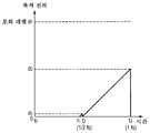
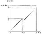
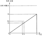
수문 모드에서, 예를 들어, 도 9 내지 도 12에 도시된 바와 같이, t4와 t5 사이의 시간을 1 프레임의 노광 시간 t0 내지 t6의 1/16로 설정한다. 그리고, 시간 t4에 축적 전하 dM 이상의 전하를 리셋하고, 다시 t4와 t5 사이에 노광을 행하고, 시간 t5에 축적 전하 dM 이상의 전하를 리셋한다. 그 후, 축적 전하 dM에 전하를 더 축적하여 추가하도록, t5와 t6 사이에 노광을 행하고, 시간 t6에 축적 전하 0 이상의 전하를 리셋한다. In the hydrological mode, for example, as shown in Figs. 9 to 12, the time between t 4 and t 5 is set to 1/16 of the exposure time t 0 to t 6 of one frame. Then, at a time t 4 , the charge of the accumulated charge d M or more is reset, and exposure is performed again between t 4 and t 5 , and at a time t 5 , the charge of the accumulated charge d M or more is reset. Thereafter, exposure is performed between t 5 and t 6 to further accumulate and add the charge to the accumulated charge d M , and reset the charge of the accumulated
그리고, t4와 t5 사이에 노광된 전하량 ds = d3 - dM(ds>0)과, 1 프레임의 노광 시간(t0 내지 t6)에 노광된 전하량에 기초하여, 1 프레임의 노광에 의해 얻어지는 전하량을 산출한다. Then, one frame is exposed based on the amount of charge ds = d 3 -d M (ds> 0) exposed between t 4 and t 5 and the amount of charge exposed during the exposure time t 0 to t 6 of one frame. The amount of charge obtained is calculated.
구체적으로, 우선, t4와 t5 사이에 노광된 전하량 ds = d3 - dM(ds>0)을 산출한다(단계 S11). 또한, 1 프레임의 노광 시간(t0 내지 t6)에 노광된 전하량 dl = d4를 산출한다(단계 S12). Specifically, first, the amount of charge ds = d 3 -d M (ds> 0) exposed between t 4 and t 5 is calculated (step S11). Further, the amount of charge dl = d 4 exposed at the exposure time t 0 to t 6 of one frame is calculated (step S12).
도 9 및 도 10에 도시된 바와 같이, 시간 t4에 축적 전하 dM 이상의 전하가 축적되는 경우, t4와 t5 사이에 노광된 전하량 ds를 상수 배로 함으로써, 1 프레임의 노광 시간에 얻어지는 본래의 전하량을 산출한다. 한편, 도 11 및 도 12에 도시된 바와 같이, 시간 t4에 축적 전하 dM 미만의 전하가 축적되는 경우, 시간 t4에 전하가 리셋되지 않는다. 따라서, t4와 t5 사이에 노광된 전하량 ds와, 1 프레임의 노광 시간(t0 내지 t6)에 노광된 전하량 dl에 기초하여, 1 프레임의 노광 시간에 얻어지는 본래의 전하량을 산출한다. As shown in Figs. 9 and 10, in the case where charges of accumulated charge d M or more accumulate at time t 4 , the original amount obtained at the exposure time of one frame by multiplying the amount of charge ds exposed between t 4 and t 5 by a constant multiple Calculate the amount of charge. On the other hand, as shown in Figs. 11 and 12, if the time t 4 is the charge of the accumulated charge under d M stored in, but not the charge is reset in time t 4. Therefore, based on the charge amount ds exposed between t 4 and t 5 and the charge amount dl exposed in the exposure time t 0 to t 6 of one frame, the original charge amount obtained in the exposure time of one frame is calculated.
예를 들어, t4와 t5 사이의 시간을 1 프레임의 노광 시간 t0 내지 t6의 1/16로 설정할 경우, ds + dl이 16ds 이상인지의 여부를 판단한다(단계 S13). 그리고, ds + dl이 16ds 이상인 경우는, 예를 들어, 도 11 및 도 12에 도시된 경우이고, ds + dl을 1 프레임의 노광 시간에 얻어지는 본래의 전하량이라고 결정한다(단계 S14). 한편, ds + dl이 16ds 미만인 경우는, 예를 들어, 도 9 및 도 10에 도시된 경우이고, 16ds를 1 프레임의 노광 시간에 얻어지는 본래의 전하량이라고 결정한다(단계 S15). For example, when the time between t 4 and t 5 is set to 1/16 of the exposure time t 0 to t 6 of one frame, it is determined whether ds + dl is 16ds or more (step S13). And when ds + dl is 16ds or more, it is the case shown in FIG. 11 and FIG. 12, for example, and it determines with ds + dl as the original electric charge amount obtained at the exposure time of one frame (step S14). On the other hand, when ds + dl is less than 16ds, for example, it is the case shown in Figs. 9 and 10, and 16ds is determined to be the original amount of electric charge obtained at the exposure time of one frame (step S15).
이어서, 복수회 노광 모드에 있어서의 축적 전하량의 산출에 대해서 설명한다. Next, the calculation of the accumulated charge amount in the plurality of exposure modes will be described.
복수회 노광 모드에서는, 예를 들어, 도 7 및 도 8에 도시된 바와 같이, 제1 절반 기간의 t1 내지 t2의 노광 시간을 제2 절반 기간의 t2 내지 t3의 노광 시간의 1/16로 설정한다. 그리고, 시간 t2와 시간 t3에 축적 전하 0 이상의 전하를 리셋한다. 그 후, t1과 t2 사이에 노광된 전하량 d1과, t2와 t3 사이에 노광된 전하량 d2(축적 전하가 포화 레벨에 도달하지 않은 경우)를 사용하여, 1 프레임의 노광 시간에 얻어지는 본래의 전하량을 산출한다. 도 7 및 도 8에 도시된 예에서는, 제2 절반 기간의 t2 내지 t3의 노광 시간을 1/2fs로 설정할 경우를 나타내지만, 복수회 노광 모드에 있어서, 노광 시간은 이 예로 한정되지 않고, 노광 시간은 자유롭게 설정될 수 있다. 예를 들어, 제1 절반 기간의 t1 내지 t2의 노광 시간과, 제2 절반 기간의 t2 내지 t3의 노광 시간을 더 단축할 수 있다. 또한, 노광 동작의 횟수도 2회로 한정되지 않고, 노광 동작은 3회 이상 행해질 수 있다. 이것은, 수문 모드와는 달리, 아이리스(조리개)를 사용하지 않고, 밝은 촬영 신에서도 본래의 전하량을 산출할 수 있게 한다. In the multiple exposure mode, for example, as shown in FIGS. 7 and 8, the exposure time of t 1 to t 2 of the first half period is set to 1 of the exposure time of t 2 to t 3 of the second half period. Set to / 16. Then, at the time t 2 and the time t 3 , the charge of 0 or more of the accumulated charge is reset. Then, the exposure time of one frame using the amount of charge d 1 exposed between t 1 and t 2 and the amount of charge d 2 exposed between t 2 and t 3 (when the accumulated charge has not reached the saturation level) The original charge amount obtained at is calculated. In the example shown in FIG. 7 and FIG. 8, the case where the exposure time of t 2 to t 3 in the second half period is set to 1/2 fs is shown. However, in the multiple times exposure mode, the exposure time is not limited to this example. The exposure time can be freely set. For example, the exposure time of t 1 to t 2 of the first half period and the exposure time of t 2 to t 3 of the second half period can be further shortened. In addition, the number of exposure operations is not limited to two times, and the exposure operation can be performed three or more times. Unlike the hydrological mode, this makes it possible to calculate the original charge amount even in a bright shooting scene without using an iris (aperture).
어두운 촬영 신에 있어서, 복수회 노광 모드에서는 노광 시간을 최장 기간 1/2fs로만 설정할 수 있지만, 수문 모드에서는 노광 시간을 최장 기간 1fs로 설정할 수 있다. 그 결과, 본 실시예에서는, 화면 전체가 어두울 때 수문 모드를 사용하기 때문에, 복수회 노광 모드를 사용하는 경우에 비해, 암부의 감도를 향상시킬 수 있다. In dark imaging scenes, the exposure time can be set only to the
[촬상 장치][Imaging device]
본 실시예에 따른 CMOS 이미지 센서(10)는, 디지털 스틸 카메라나 비디오 카메라 등의 촬상 장치(image pickup device)에 있어서, 그의 촬상 디바이스(imaging device)(화상 입력 디바이스)로서 사용하기에 적합하다. The
여기서, 촬상 장치란, 촬상 디바이스로서의 고체 촬상 장치, 고체 촬상 장치의 촬상 영역(수광면) 상에 피사체의 상의 광을 결상시키는 광학계, 및 고체 촬상 장치의 신호 처리부를 포함하는 카메라 모듈(예를 들어, 셀룰러 텔레폰 등의 전자 기기에 탑재되어 사용됨), 및 카메라 모듈이 탑재된 디지털 스틸 카메라와 비디오 카메라 등의 카메라 시스템을 칭한다. Here, the imaging device is a camera module including a solid-state imaging device as an imaging device, an optical system that forms an image of an image of a subject on an imaging area (light receiving surface) of a solid-state imaging device, and a signal processing unit of a solid-state imaging device (for example, , A camera system such as a digital still camera and a video camera equipped with an electronic device such as a cellular telephone) and a camera module.
도 18은 본 발명의 실시예에 따른 촬상 장치의 구성의 예를 도시하는 블록도이다. 도 18 도시된 바와 같이, 본 발명의 실시예에 따른 촬상 장치는, 렌즈(81)를 포함하는 광학계, 촬상 디바이스(촬상부)(82), 카메라 신호 처리부(83) 등으로 형성된다. 18 is a block diagram illustrating an example of a configuration of an imaging device according to an embodiment of the present invention. As shown in FIG. 18, the imaging device according to the embodiment of the present invention is formed of an optical system including a
렌즈(81)는 피사체로부터의 상의 광을 촬상 디바이스(82)의 촬상 영역에 결상한다. 촬상 디바이스(82)는 렌즈(81)에 의해 촬상 영역에 결상된 상의 광을 화소 단위로 전기 신호로 변환해서 얻어지는 화상 신호를 출력한다. 촬상 디바이스(82)로서, 본 실시예에 따른 CMOS 이미지 센서(10)가 사용된다. 카메라 신호 처리부(83)는, 촬상 디바이스(82)로부터 출력되는 화상 신호에 대하여 다양한 신호 처리를 행한다. The
카메라 신호 처리부(83)는 신호 처리부의 예이며, 모드를 수문 모드와 복수회 노광 모드 간에 전환하여, 수문 모드 또는 복수회 노광 모드에 있어서의 신호 레벨을 결정한다. 또한, 카메라 신호 처리부(83)는, 전하에 기초하는 검출값에 따라 신호 레벨을 조정하는 게인을 결정하고, 게인에 기초하여, 수문 모드와 복수회 노광 모드 간에 전환을 행한다. The camera
이상, 첨부 도면을 참조하여 본 발명의 바람직한 실시예에 대해서 상세하게 설명했지만, 본 발명은 결코 이러한 예들로 한정되지 않는다. 본 발명이 속하는 기술 분야에 있어서의 통상의 지식을 가진 자이면, 본 발명의 실시예에 따른 기술 사상의 범위 내에서 다양한 변형 또는 수정을 도출할 수 있는 것은 명확하고, 이러한 변형 또는 수정은 당연히 본 발명의 기술적 범위에 포함되는 것으로 해석되어야 한다는 것을 이해할 것이다.As mentioned above, although preferred embodiment of this invention was described in detail with reference to an accompanying drawing, this invention is not limited to these examples at all. Those skilled in the art to which the present invention pertains are apparent that various modifications or changes can be made within the scope of the technical idea according to the embodiments of the present invention, and such modifications or modifications are naturally described. It will be understood that it should be interpreted as being included in the technical scope of the invention.
본 발명은 2010년 9월 28일자로 일본 특허청에 출원된 일본 우선권 특허 출원 제2010-216285호에 개시된 내용에 관한 요지를 포함하고, 그 전체 내용이 본 명세서에 참조되어 포괄된다.The present invention includes the gist of the contents disclosed in Japanese Priority Patent Application No. 2010-216285 filed with the Japan Patent Office on September 28, 2010, the entire contents of which are incorporated herein by reference.
10: CMOS 이미지 센서
11: 화소 어레이부
12, 13A, 13B: 행 선택 회로
13: 선행 선택 회로
14: 논리 회로
15: 드라이버 회로
16: 컨트롤러 유닛
17: 전압 공급 회로
18: 컬럼 회로
19: 수평 주사 회로
20: 단위 화소
21: 포토다이오드
22: 전송 트랜지스터
23: 리셋 트랜지스터
24: 증폭 트랜지스터
25: 선택 트랜지스터
26: FD(플로팅 디퓨전)부 10: CMOS image sensor
11: pixel array unit
12, 13A, 13B: Row Select Circuit
13: precedent selection circuit
14: logic circuit
15: driver circuit
16: controller unit
17: voltage supply circuit
18: column circuit
19: horizontal scanning circuit
20: module pixel
21: photodiode
22: transfer transistor
23: reset transistor
24: amplifying transistor
25: select transistor
26: floating diffusion part
Claims (6)
광을 전하로 변환하는 광전 변환 소자를 각각 갖는 단위 화소들이 행렬로 2차원적으로 배치된 화소 어레이부, 및
제1 노광 기간에 미리 결정된 축적 전하 이상으로 상기 단위 화소들에 축적된 전하에 기초하는 제1 전하량, 또는 상기 제1 노광 기간을 포함하는 제2 노광 기간에 상기 단위 화소들에 축적된 모든 전하에 기초하는 제2 전하량에 따라 신호 레벨을 결정하는 모드인 수문 모드와, 복수회의 노광 기간에 상기 단위 화소들에 축적된 모든 전하에 기초하는 복수의 전하량에 따라 신호 레벨을 결정하는 모드인 복수회 노광 모드 중 어느 하나를 사용하여, 상기 신호 레벨을 결정하는 신호 처리부를 포함하는, 화상 처리 장치. As an image processing apparatus,
A pixel array unit in which unit pixels each having photoelectric conversion elements for converting light into charges are two-dimensionally arranged in a matrix; and
The first charge amount based on the charge accumulated in the unit pixels above the predetermined accumulated charge in the first exposure period, or all the charges accumulated in the unit pixels in the second exposure period including the first exposure period. A plurality of exposures, a hydrological mode that is a mode for determining a signal level in accordance with a second charge amount based on and a mode for determining a signal level in accordance with a plurality of charges based on all charges accumulated in the unit pixels in a plurality of exposure periods. And a signal processing unit for determining the signal level using any one of modes.
상기 신호 처리부는, 상기 전하에 기초하는 검출값에 따라 상기 신호 레벨을 조정하는 게인을 결정하고, 상기 게인에 기초하여 모드를 상기 수문 모드와 상기 복수회 노광 모드 중 어느 하나로 전환하는, 화상 처리 장치. The method of claim 1,
The signal processing unit determines a gain for adjusting the signal level according to a detection value based on the charge, and switches the mode to either the hydrological mode or the multiple exposure mode based on the gain. .
상기 모드가 상기 수문 모드일 때, 상기 신호 처리부는, 상기 게인이 0이 될 경우에 상기 모드를 상기 복수회 노광 모드로 전환하는, 화상 처리 장치. The method of claim 2,
And the signal processing unit switches the mode to the plurality of exposure modes when the gain becomes zero when the mode is the hydrological mode.
상기 모드가 상기 복수회 노광 모드일 때, 상기 신호 처리부는, 상기 게인이 미리 설정된 히스테리시스 이상이 될 경우에 상기 모드를 상기 수문 모드로 전환하는, 화상 처리 장치. The method of claim 2,
And the signal processing unit switches the mode to the hydrological mode when the gain is equal to or greater than a preset hysteresis when the mode is the plurality of exposure modes.
광전 변환 소자를 각각 갖는 단위 화소들이 행렬로 2차원적으로 배치된 화소 어레이부를 이용하여 광을 전하로 변환하는 단계, 및
신호 처리부가, 제1 노광 기간에 미리 결정된 축적 전하 이상으로 상기 단위 화소들에 축적된 전하에 기초하는 제1 전하량, 또는 상기 제1 노광 기간을 포함하는 제2 노광 기간에 상기 단위 화소들에 축적된 모든 전하에 기초하는 제2 전하량에 따라 신호 레벨을 결정하는 모드인 수문 모드와, 복수회의 노광 기간에 상기 단위 화소들에 축적된 모든 전하에 기초하는 복수의 전하량에 따라 신호 레벨을 결정하는 모드인 복수회 노광 모드 중 어느 하나를 사용하여, 상기 신호 레벨을 결정하는 단계를 포함하는, 화상 처리 방법. As the image processing method,
Converting light into electric charge using a pixel array unit in which unit pixels each having a photoelectric conversion element are two-dimensionally arranged in a matrix, and
The signal processing unit accumulates in the unit pixels in the first exposure amount based on the charge accumulated in the unit pixels above the predetermined accumulation charge in the first exposure period, or in the second exposure period including the first exposure period. The hydrological mode is a mode for determining the signal level in accordance with the second charge amount based on all the charged charges, and the mode for determining the signal level according to the plurality of charge amounts based on all the charges accumulated in the unit pixels in a plurality of exposure periods. Determining the signal level using any one of a plurality of exposure modes.
신호 처리부가, 제1 노광 기간에 미리 결정된 축적 전하 이상으로 상기 단위 화소들에 축적된 전하에 기초하는 제1 전하량, 또는 상기 제1 노광 기간을 포함하는 제2 노광 기간에 상기 단위 화소들에 축적된 모든 전하에 기초하는 제2 전하량에 따라 신호 레벨을 결정하는 모드인 수문 모드와, 복수회의 노광 기간에 상기 단위 화소들에 축적된 모든 전하에 기초하는 복수의 전하량에 따라 신호 레벨을 결정하는 모드인 복수회 노광 모드 중 어느 하나를 사용하여, 상기 신호 레벨을 결정하는 단계를 포함하는 처리를, 컴퓨터에 실행시키기 위한 프로그램. Converting light into electric charge using a pixel array unit in which unit pixels each having a photoelectric conversion element are two-dimensionally arranged in a matrix, and
The signal processing unit accumulates in the unit pixels in the first exposure amount based on the charge accumulated in the unit pixels above the predetermined accumulation charge in the first exposure period, or in the second exposure period including the first exposure period. The hydrological mode is a mode for determining the signal level in accordance with the second charge amount based on all the charged charges, and the mode for determining the signal level according to the plurality of charge amounts based on all the charges accumulated in the unit pixels in a plurality of exposure periods. A program for causing a computer to execute a process comprising determining the signal level using any one of a plurality of exposure modes.
Applications Claiming Priority (2)
| Application Number | Priority Date | Filing Date | Title |
|---|---|---|---|
| JPJP-P-2010-216285 | 2010-09-28 | ||
| JP2010216285A JP5569298B2 (en) | 2010-09-28 | 2010-09-28 | Image processing apparatus, image processing method, and program |
Publications (1)
| Publication Number | Publication Date |
|---|---|
| KR20120032425A true KR20120032425A (en) | 2012-04-05 |
Family
ID=45870290
Family Applications (1)
| Application Number | Title | Priority Date | Filing Date |
|---|---|---|---|
| KR1020110094614A Withdrawn KR20120032425A (en) | 2010-09-28 | 2011-09-20 | Image processing apparatus, image processing method, and image processing program |
Country Status (5)
| Country | Link |
|---|---|
| US (1) | US8547452B2 (en) |
| JP (1) | JP5569298B2 (en) |
| KR (1) | KR20120032425A (en) |
| CN (1) | CN102547164B (en) |
| TW (1) | TW201223273A (en) |
Families Citing this family (7)
| Publication number | Priority date | Publication date | Assignee | Title |
|---|---|---|---|---|
| KR101475285B1 (en) * | 2010-08-12 | 2014-12-23 | 연세대학교 산학협력단 | Cmos image sensor and operation method thereof |
| FR2992813A1 (en) * | 2012-07-02 | 2014-01-03 | St Microelectronics Grenoble 2 | METHOD FOR CONTROLLING A CMOS PIXEL |
| CN106454156B (en) * | 2015-08-10 | 2019-07-19 | 原相科技股份有限公司 | Image sensor and method of operation |
| CN108700664A (en) * | 2017-02-06 | 2018-10-23 | 松下知识产权经营株式会社 | Three-dimensional motion acquisition device and three-dimensional motion adquisitiones |
| JP2020020675A (en) * | 2018-08-01 | 2020-02-06 | ソニーセミコンダクタソリューションズ株式会社 | Measuring device |
| CN111565265A (en) * | 2019-02-14 | 2020-08-21 | 上海银镐环境科技有限公司 | Frequency difference value camera device |
| CN114302024B (en) * | 2021-12-28 | 2023-04-18 | 北京理工大学 | Electron bombardment CMOS imaging method and device |
Family Cites Families (8)
| Publication number | Priority date | Publication date | Assignee | Title |
|---|---|---|---|---|
| US6977685B1 (en) * | 1999-02-26 | 2005-12-20 | Massachusetts Institute Of Technology | Single-chip imager system with programmable dynamic range |
| US6963370B2 (en) * | 2001-09-24 | 2005-11-08 | The Board Of Trustees Of The Leland Stanford Junior University | Method for improving SNR in low illumination conditions in a CMOS video sensor system using a self-resetting digital pixel |
| JP2003158669A (en) * | 2001-11-21 | 2003-05-30 | Olympus Optical Co Ltd | Image pickup device |
| US7596280B2 (en) * | 2005-09-29 | 2009-09-29 | Apple Inc. | Video acquisition with integrated GPU processing |
| US7812301B2 (en) * | 2005-10-28 | 2010-10-12 | Sony Corporation | Solid-state imaging device, method of driving solid-state imaging device and imaging apparatus |
| JP4973115B2 (en) * | 2006-10-16 | 2012-07-11 | ソニー株式会社 | Solid-state imaging device, driving method of solid-state imaging device, and imaging device |
| JP4905187B2 (en) * | 2007-03-09 | 2012-03-28 | ソニー株式会社 | Image processing apparatus, imaging apparatus, image processing method, and computer program |
| JP5106052B2 (en) * | 2007-11-08 | 2012-12-26 | キヤノン株式会社 | Solid-state imaging device, imaging system, and solid-state imaging device driving method |
-
2010
- 2010-09-28 JP JP2010216285A patent/JP5569298B2/en not_active Expired - Fee Related
-
2011
- 2011-09-20 TW TW100133774A patent/TW201223273A/en unknown
- 2011-09-20 KR KR1020110094614A patent/KR20120032425A/en not_active Withdrawn
- 2011-09-20 US US13/236,754 patent/US8547452B2/en not_active Expired - Fee Related
- 2011-09-21 CN CN201110294348.2A patent/CN102547164B/en not_active Expired - Fee Related
Also Published As
| Publication number | Publication date |
|---|---|
| JP5569298B2 (en) | 2014-08-13 |
| TW201223273A (en) | 2012-06-01 |
| CN102547164A (en) | 2012-07-04 |
| JP2012074783A (en) | 2012-04-12 |
| US8547452B2 (en) | 2013-10-01 |
| CN102547164B (en) | 2016-09-28 |
| US20120075499A1 (en) | 2012-03-29 |
Similar Documents
| Publication | Publication Date | Title |
|---|---|---|
| JP4862473B2 (en) | Solid-state imaging device, driving method of solid-state imaging device, and imaging device | |
| JP4973115B2 (en) | Solid-state imaging device, driving method of solid-state imaging device, and imaging device | |
| JP5223953B2 (en) | Solid-state imaging device, driving method of solid-state imaging device, and imaging device | |
| US7812301B2 (en) | Solid-state imaging device, method of driving solid-state imaging device and imaging apparatus | |
| JP4931233B2 (en) | Imaging apparatus and processing method thereof | |
| US8174590B2 (en) | Image pickup apparatus and image pickup method | |
| KR101939402B1 (en) | Solid-state imaging device and driving method thereof, and electronic apparatus using the same | |
| US8547452B2 (en) | Image processing apparatus, image processing method, and image processing program | |
| JP2007020156A (en) | Imaging apparatus and imaging system | |
| US7550704B2 (en) | Solid state imaging device, method of driving solid state imaging device, and image pickup apparatus | |
| JP4834345B2 (en) | IMAGING DEVICE, ITS CONTROL METHOD, PROGRAM, AND STORAGE MEDIUM | |
| KR20070091104A (en) | Solid-state imaging device | |
| JP2007097127A (en) | Solid-state imaging device | |
| JP2006217548A (en) | Solid-state imaging device | |
| JP2007208885A (en) | Imaging unit and image sensor | |
| JP3827146B2 (en) | Solid-state imaging device and driving method of solid-state imaging device | |
| JP5051994B2 (en) | Solid-state imaging device, driving method of solid-state imaging device, and imaging device | |
| JP2016178408A (en) | Solid-state image pickup device, driving method for the same and imaging system | |
| JP2006217421A (en) | Solid-state imaging device | |
| JP2013243783A (en) | Imaging apparatus and imaging system | |
| JP2004112474A (en) | Solid-state imaging device | |
| JP2006197229A (en) | Imaging device and camera | |
| JP5362055B2 (en) | Image pickup apparatus, image pickup system, and image pickup apparatus control method | |
| JP2005303592A (en) | Solid-state imaging device and signal processing method thereof |
Legal Events
| Date | Code | Title | Description |
|---|---|---|---|
| PA0109 | Patent application |
Patent event code: PA01091R01D Comment text: Patent Application Patent event date: 20110920 |
|
| PG1501 | Laying open of application | ||
| PC1203 | Withdrawal of no request for examination | ||
| WITN | Application deemed withdrawn, e.g. because no request for examination was filed or no examination fee was paid |