KR20120034560A - 파워 모듈 및 그 제조방법 - Google Patents
파워 모듈 및 그 제조방법 Download PDFInfo
- Publication number
- KR20120034560A KR20120034560A KR1020110095014A KR20110095014A KR20120034560A KR 20120034560 A KR20120034560 A KR 20120034560A KR 1020110095014 A KR1020110095014 A KR 1020110095014A KR 20110095014 A KR20110095014 A KR 20110095014A KR 20120034560 A KR20120034560 A KR 20120034560A
- Authority
- KR
- South Korea
- Prior art keywords
- wiring member
- wiring
- power element
- insulating substrate
- sealing material
- Prior art date
- Legal status (The legal status is an assumption and is not a legal conclusion. Google has not performed a legal analysis and makes no representation as to the accuracy of the status listed.)
- Abandoned
Links
Images




Classifications
-
- H—ELECTRICITY
- H10—SEMICONDUCTOR DEVICES; ELECTRIC SOLID-STATE DEVICES NOT OTHERWISE PROVIDED FOR
- H10W—GENERIC PACKAGES, INTERCONNECTIONS, CONNECTORS OR OTHER CONSTRUCTIONAL DETAILS OF DEVICES COVERED BY CLASS H10
- H10W74/00—Encapsulations, e.g. protective coatings
- H10W74/10—Encapsulations, e.g. protective coatings characterised by their shape or disposition
- H10W74/111—Encapsulations, e.g. protective coatings characterised by their shape or disposition the semiconductor body being completely enclosed
- H10W74/114—Encapsulations, e.g. protective coatings characterised by their shape or disposition the semiconductor body being completely enclosed by a substrate and the encapsulations
-
- H—ELECTRICITY
- H10—SEMICONDUCTOR DEVICES; ELECTRIC SOLID-STATE DEVICES NOT OTHERWISE PROVIDED FOR
- H10W—GENERIC PACKAGES, INTERCONNECTIONS, CONNECTORS OR OTHER CONSTRUCTIONAL DETAILS OF DEVICES COVERED BY CLASS H10
- H10W72/00—Interconnections or connectors in packages
-
- H—ELECTRICITY
- H10—SEMICONDUCTOR DEVICES; ELECTRIC SOLID-STATE DEVICES NOT OTHERWISE PROVIDED FOR
- H10W—GENERIC PACKAGES, INTERCONNECTIONS, CONNECTORS OR OTHER CONSTRUCTIONAL DETAILS OF DEVICES COVERED BY CLASS H10
- H10W74/00—Encapsulations, e.g. protective coatings
- H10W74/10—Encapsulations, e.g. protective coatings characterised by their shape or disposition
- H10W74/111—Encapsulations, e.g. protective coatings characterised by their shape or disposition the semiconductor body being completely enclosed
- H10W74/121—Encapsulations, e.g. protective coatings characterised by their shape or disposition the semiconductor body being completely enclosed by multiple encapsulations, e.g. by a thin protective coating and a thick encapsulation
-
- H—ELECTRICITY
- H10—SEMICONDUCTOR DEVICES; ELECTRIC SOLID-STATE DEVICES NOT OTHERWISE PROVIDED FOR
- H10W—GENERIC PACKAGES, INTERCONNECTIONS, CONNECTORS OR OTHER CONSTRUCTIONAL DETAILS OF DEVICES COVERED BY CLASS H10
- H10W76/00—Containers; Fillings or auxiliary members therefor; Seals
- H10W76/40—Fillings or auxiliary members in containers, e.g. centering rings
- H10W76/42—Fillings
- H10W76/47—Solid or gel fillings
-
- H—ELECTRICITY
- H10—SEMICONDUCTOR DEVICES; ELECTRIC SOLID-STATE DEVICES NOT OTHERWISE PROVIDED FOR
- H10W—GENERIC PACKAGES, INTERCONNECTIONS, CONNECTORS OR OTHER CONSTRUCTIONAL DETAILS OF DEVICES COVERED BY CLASS H10
- H10W90/00—Package configurations
-
- H—ELECTRICITY
- H10—SEMICONDUCTOR DEVICES; ELECTRIC SOLID-STATE DEVICES NOT OTHERWISE PROVIDED FOR
- H10W—GENERIC PACKAGES, INTERCONNECTIONS, CONNECTORS OR OTHER CONSTRUCTIONAL DETAILS OF DEVICES COVERED BY CLASS H10
- H10W72/00—Interconnections or connectors in packages
- H10W72/071—Connecting or disconnecting
- H10W72/073—Connecting or disconnecting of die-attach connectors
- H10W72/07351—Connecting or disconnecting of die-attach connectors characterised by changes in properties of the die-attach connectors during connecting
- H10W72/07354—Connecting or disconnecting of die-attach connectors characterised by changes in properties of the die-attach connectors during connecting changes in dispositions
-
- H—ELECTRICITY
- H10—SEMICONDUCTOR DEVICES; ELECTRIC SOLID-STATE DEVICES NOT OTHERWISE PROVIDED FOR
- H10W—GENERIC PACKAGES, INTERCONNECTIONS, CONNECTORS OR OTHER CONSTRUCTIONAL DETAILS OF DEVICES COVERED BY CLASS H10
- H10W72/00—Interconnections or connectors in packages
- H10W72/071—Connecting or disconnecting
- H10W72/075—Connecting or disconnecting of bond wires
- H10W72/07531—Techniques
- H10W72/07532—Compression bonding, e.g. thermocompression bonding
- H10W72/07533—Ultrasonic bonding, e.g. thermosonic bonding
-
- H—ELECTRICITY
- H10—SEMICONDUCTOR DEVICES; ELECTRIC SOLID-STATE DEVICES NOT OTHERWISE PROVIDED FOR
- H10W—GENERIC PACKAGES, INTERCONNECTIONS, CONNECTORS OR OTHER CONSTRUCTIONAL DETAILS OF DEVICES COVERED BY CLASS H10
- H10W72/00—Interconnections or connectors in packages
- H10W72/30—Die-attach connectors
- H10W72/341—Dispositions of die-attach connectors, e.g. layouts
- H10W72/347—Dispositions of multiple die-attach connectors
-
- H—ELECTRICITY
- H10—SEMICONDUCTOR DEVICES; ELECTRIC SOLID-STATE DEVICES NOT OTHERWISE PROVIDED FOR
- H10W—GENERIC PACKAGES, INTERCONNECTIONS, CONNECTORS OR OTHER CONSTRUCTIONAL DETAILS OF DEVICES COVERED BY CLASS H10
- H10W72/00—Interconnections or connectors in packages
- H10W72/50—Bond wires
-
- H—ELECTRICITY
- H10—SEMICONDUCTOR DEVICES; ELECTRIC SOLID-STATE DEVICES NOT OTHERWISE PROVIDED FOR
- H10W—GENERIC PACKAGES, INTERCONNECTIONS, CONNECTORS OR OTHER CONSTRUCTIONAL DETAILS OF DEVICES COVERED BY CLASS H10
- H10W72/00—Interconnections or connectors in packages
- H10W72/50—Bond wires
- H10W72/531—Shapes of wire connectors
- H10W72/533—Cross-sectional shape
- H10W72/534—Cross-sectional shape being rectangular
-
- H—ELECTRICITY
- H10—SEMICONDUCTOR DEVICES; ELECTRIC SOLID-STATE DEVICES NOT OTHERWISE PROVIDED FOR
- H10W—GENERIC PACKAGES, INTERCONNECTIONS, CONNECTORS OR OTHER CONSTRUCTIONAL DETAILS OF DEVICES COVERED BY CLASS H10
- H10W72/00—Interconnections or connectors in packages
- H10W72/50—Bond wires
- H10W72/531—Shapes of wire connectors
- H10W72/5363—Shapes of wire connectors the connected ends being wedge-shaped
-
- H—ELECTRICITY
- H10—SEMICONDUCTOR DEVICES; ELECTRIC SOLID-STATE DEVICES NOT OTHERWISE PROVIDED FOR
- H10W—GENERIC PACKAGES, INTERCONNECTIONS, CONNECTORS OR OTHER CONSTRUCTIONAL DETAILS OF DEVICES COVERED BY CLASS H10
- H10W72/00—Interconnections or connectors in packages
- H10W72/50—Bond wires
- H10W72/541—Dispositions of bond wires
- H10W72/5434—Dispositions of bond wires the connected ends being on auxiliary connecting means on bond pads, e.g. on other bond wires
-
- H—ELECTRICITY
- H10—SEMICONDUCTOR DEVICES; ELECTRIC SOLID-STATE DEVICES NOT OTHERWISE PROVIDED FOR
- H10W—GENERIC PACKAGES, INTERCONNECTIONS, CONNECTORS OR OTHER CONSTRUCTIONAL DETAILS OF DEVICES COVERED BY CLASS H10
- H10W72/00—Interconnections or connectors in packages
- H10W72/50—Bond wires
- H10W72/551—Materials of bond wires
- H10W72/552—Materials of bond wires comprising metals or metalloids, e.g. silver
- H10W72/5524—Materials of bond wires comprising metals or metalloids, e.g. silver comprising aluminium [Al]
-
- H—ELECTRICITY
- H10—SEMICONDUCTOR DEVICES; ELECTRIC SOLID-STATE DEVICES NOT OTHERWISE PROVIDED FOR
- H10W—GENERIC PACKAGES, INTERCONNECTIONS, CONNECTORS OR OTHER CONSTRUCTIONAL DETAILS OF DEVICES COVERED BY CLASS H10
- H10W72/00—Interconnections or connectors in packages
- H10W72/50—Bond wires
- H10W72/551—Materials of bond wires
- H10W72/552—Materials of bond wires comprising metals or metalloids, e.g. silver
- H10W72/5525—Materials of bond wires comprising metals or metalloids, e.g. silver comprising copper [Cu]
-
- H—ELECTRICITY
- H10—SEMICONDUCTOR DEVICES; ELECTRIC SOLID-STATE DEVICES NOT OTHERWISE PROVIDED FOR
- H10W—GENERIC PACKAGES, INTERCONNECTIONS, CONNECTORS OR OTHER CONSTRUCTIONAL DETAILS OF DEVICES COVERED BY CLASS H10
- H10W72/00—Interconnections or connectors in packages
- H10W72/50—Bond wires
- H10W72/59—Bond pads specially adapted therefor
-
- H—ELECTRICITY
- H10—SEMICONDUCTOR DEVICES; ELECTRIC SOLID-STATE DEVICES NOT OTHERWISE PROVIDED FOR
- H10W—GENERIC PACKAGES, INTERCONNECTIONS, CONNECTORS OR OTHER CONSTRUCTIONAL DETAILS OF DEVICES COVERED BY CLASS H10
- H10W72/00—Interconnections or connectors in packages
- H10W72/851—Dispositions of multiple connectors or interconnections
- H10W72/874—On different surfaces
- H10W72/884—Die-attach connectors and bond wires
-
- H—ELECTRICITY
- H10—SEMICONDUCTOR DEVICES; ELECTRIC SOLID-STATE DEVICES NOT OTHERWISE PROVIDED FOR
- H10W—GENERIC PACKAGES, INTERCONNECTIONS, CONNECTORS OR OTHER CONSTRUCTIONAL DETAILS OF DEVICES COVERED BY CLASS H10
- H10W72/00—Interconnections or connectors in packages
- H10W72/90—Bond pads, in general
- H10W72/951—Materials of bond pads
- H10W72/952—Materials of bond pads comprising metals or metalloids, e.g. PbSn, Ag or Cu
-
- H—ELECTRICITY
- H10—SEMICONDUCTOR DEVICES; ELECTRIC SOLID-STATE DEVICES NOT OTHERWISE PROVIDED FOR
- H10W—GENERIC PACKAGES, INTERCONNECTIONS, CONNECTORS OR OTHER CONSTRUCTIONAL DETAILS OF DEVICES COVERED BY CLASS H10
- H10W74/00—Encapsulations, e.g. protective coatings
-
- H—ELECTRICITY
- H10—SEMICONDUCTOR DEVICES; ELECTRIC SOLID-STATE DEVICES NOT OTHERWISE PROVIDED FOR
- H10W—GENERIC PACKAGES, INTERCONNECTIONS, CONNECTORS OR OTHER CONSTRUCTIONAL DETAILS OF DEVICES COVERED BY CLASS H10
- H10W90/00—Package configurations
- H10W90/701—Package configurations characterised by the relative positions of pads or connectors relative to package parts
- H10W90/731—Package configurations characterised by the relative positions of pads or connectors relative to package parts of die-attach connectors
- H10W90/734—Package configurations characterised by the relative positions of pads or connectors relative to package parts of die-attach connectors between a chip and a stacked insulating package substrate, interposer or RDL
-
- H—ELECTRICITY
- H10—SEMICONDUCTOR DEVICES; ELECTRIC SOLID-STATE DEVICES NOT OTHERWISE PROVIDED FOR
- H10W—GENERIC PACKAGES, INTERCONNECTIONS, CONNECTORS OR OTHER CONSTRUCTIONAL DETAILS OF DEVICES COVERED BY CLASS H10
- H10W90/00—Package configurations
- H10W90/701—Package configurations characterised by the relative positions of pads or connectors relative to package parts
- H10W90/751—Package configurations characterised by the relative positions of pads or connectors relative to package parts of bond wires
- H10W90/753—Package configurations characterised by the relative positions of pads or connectors relative to package parts of bond wires between laterally-adjacent chips
-
- H—ELECTRICITY
- H10—SEMICONDUCTOR DEVICES; ELECTRIC SOLID-STATE DEVICES NOT OTHERWISE PROVIDED FOR
- H10W—GENERIC PACKAGES, INTERCONNECTIONS, CONNECTORS OR OTHER CONSTRUCTIONAL DETAILS OF DEVICES COVERED BY CLASS H10
- H10W90/00—Package configurations
- H10W90/701—Package configurations characterised by the relative positions of pads or connectors relative to package parts
- H10W90/751—Package configurations characterised by the relative positions of pads or connectors relative to package parts of bond wires
- H10W90/754—Package configurations characterised by the relative positions of pads or connectors relative to package parts of bond wires between a chip and a stacked insulating package substrate, interposer or RDL
-
- H—ELECTRICITY
- H10—SEMICONDUCTOR DEVICES; ELECTRIC SOLID-STATE DEVICES NOT OTHERWISE PROVIDED FOR
- H10W—GENERIC PACKAGES, INTERCONNECTIONS, CONNECTORS OR OTHER CONSTRUCTIONAL DETAILS OF DEVICES COVERED BY CLASS H10
- H10W90/00—Package configurations
- H10W90/701—Package configurations characterised by the relative positions of pads or connectors relative to package parts
- H10W90/761—Package configurations characterised by the relative positions of pads or connectors relative to package parts of strap connectors
- H10W90/763—Package configurations characterised by the relative positions of pads or connectors relative to package parts of strap connectors between laterally-adjacent chips
Landscapes
- Cooling Or The Like Of Semiconductors Or Solid State Devices (AREA)
- Wire Bonding (AREA)
Abstract
Description
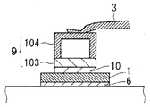
도 2는 실시형태 1에 관한 배선부재의 단면도다.
도 3은 실시형태 1에 관한 배선부재의 단면도다.
도 4는 실시형태 2에 관한 파워 모듈의 단면도다.
도 5는 실시형태 3에 관한 파워 모듈의 단면도다.
도 6은 전제기술에 관한 파워 모듈의 단면도다.
Claims (9)
- 케이스 내부에 배치된 절연 기판과,
상기 절연 기판 위에 접합된 파워 소자와,
상기 파워 소자의 표면 전극에 제1측면이 접합된, 사각형 통 형상의 금속인 제1배선부재와,
상기 제1배선부재의 상기 제1측면과 대향하는 제2측면에 접속된 배선과,
상기 절연 기판, 상기 파워 소자, 상기 제1배선부재 및 상기 배선을 덮어 상기 케이스 내부에 충전되는 밀봉재를 구비한, 파워 모듈.
- 제 1항에 있어서,
상기 제1배선부재의 열팽창율은, 상기 파워 소자의 열팽창율보다 큰, 파워 모듈.
- 제 1항 또는 제 2항에 있어서,
상기 제1배선부재는, 상기 제1측면에 대응하는 부재가, 다른 측면에 대응하는 부재보다도 열팽창율이 낮은 부재인, 파워 모듈.
- 제 1항 또는 제 2항에 있어서,
상기 밀봉재는,
상기 제1배선부재의 적어도 상기 제2측면이 노출하도록, 상기 절연 기판, 상기 파워 소자 및 상기 제1배선부재를 덮어 상기 케이스 내부에 충전되는 제1밀봉재와,
상기 제1배선부재의 적어도 상기 제2측면 및 상기 배선을 덮어, 상기 제1밀봉재 위에 더 충전되는 제2밀봉재를 구비한, 파워 모듈.
- 제 4항에 있어서,
상기 절연 기판의 표면 패턴에 제1측면이 접합된, 사각형 통 형상의 금속인 제2배선부재를 더 구비하고,
상기 제1밀봉재는, 적어도 상기 제2배선부재의 상기 제1측면과 대향하는 제2측면이 노출하도록, 상기 제2배선부재를 덮어 충전되고,
상기 제2밀봉재는, 적어도 상기 제2배선부재의 상기 제2측면을 덮어 충전되는, 파워 모듈.
- 제 1항 또는 제 2항에 있어서,
상기 밀봉재는, 에폭시 수지인, 파워 모듈.
- 제 1항 또는 제 2항에 있어서,
상기 절연 기판 위에 상기 파워 소자는 복수 배치되고,
상기 제1배선부재는 복수의 상기 파워 소자에 대응해서 구비되고, 복수의 상기 파워 소자의 각 표면 전극에 대응해서 각 상기 제1측면이 접합되고,
상기 각 제1배선부재의 각 상기 제2측면은, 서로 접합되는, 파워 모듈.
- 제 1항 또는 제 2항에 있어서,
상기 파워 소자는, 와이드 밴드갭 반도체 소자인, 파워 모듈.
- 케이스 내부에 배치된 절연 기판과,
상기 절연 기판 위에 접합된 파워 소자와,
상기 파워 소자의 표면 전극에 제1측면이 접합된, 사각형 통 형상의 금속인 제1배선부재와,
상기 제1배선부재의 상기 제1측면과 대향하는 제2측면에 접속된 배선과,
상기 절연 기판, 상기 파워 소자, 상기 제1배선부재 및 상기 배선을 덮어 상기 케이스 내부에 충전되는 밀봉재를 구비하고,
상기 밀봉재는,
상기 제1배선부재의 적어도 상기 제2측면이 노출하도록, 상기 절연 기판, 상기 파워 소자 및 상기 제1배선부재를 덮어 상기 케이스 내부에 충전되는 제1밀봉재와,
상기 제1배선부재의 적어도 상기 제2측면 및 상기 배선을 덮어, 상기 제1밀봉재 위에 더 충전되는 제2밀봉재를 구비한 파워 모듈을 제조하는 방법으로서,
(a) 상기 제1배선부재의 적어도 상기 제2측면이 노출하도록, 상기 절연 기판, 상기 파워 소자 및 상기 제1배선부재를 덮어 상기 케이스 내부에 상기 제1밀봉재를 충전하는 공정과,
(b) 상기 제1밀봉재를 충전하여 노출한 상기 제1배선부재의 상기 제2측면에, 상기 배선을 접속하는 공정과,
(c) 상기 제1배선부재의 적어도 상기 제2측면 및 상기 배선을 덮어, 상기 제1밀봉재 위에 상기 제2밀봉재를 더 충전하는 공정을 구비한, 파워 모듈의 제조방법.
Applications Claiming Priority (2)
| Application Number | Priority Date | Filing Date | Title |
|---|---|---|---|
| JPJP-P-2010-223505 | 2010-10-01 | ||
| JP2010223505A JP2012079914A (ja) | 2010-10-01 | 2010-10-01 | パワーモジュールおよびその製造方法 |
Publications (1)
| Publication Number | Publication Date |
|---|---|
| KR20120034560A true KR20120034560A (ko) | 2012-04-12 |
Family
ID=45889097
Family Applications (1)
| Application Number | Title | Priority Date | Filing Date |
|---|---|---|---|
| KR1020110095014A Abandoned KR20120034560A (ko) | 2010-10-01 | 2011-09-21 | 파워 모듈 및 그 제조방법 |
Country Status (5)
| Country | Link |
|---|---|
| US (1) | US20120080800A1 (ko) |
| JP (1) | JP2012079914A (ko) |
| KR (1) | KR20120034560A (ko) |
| CN (1) | CN102446864A (ko) |
| DE (1) | DE102011083927A1 (ko) |
Families Citing this family (15)
| Publication number | Priority date | Publication date | Assignee | Title |
|---|---|---|---|---|
| JP5656907B2 (ja) * | 2012-04-11 | 2015-01-21 | 三菱電機株式会社 | パワーモジュール |
| US9087833B2 (en) | 2012-11-30 | 2015-07-21 | Samsung Electronics Co., Ltd. | Power semiconductor devices |
| CN204991692U (zh) | 2014-11-26 | 2016-01-20 | 意法半导体股份有限公司 | 具有引线键合和烧结区域的电子器件 |
| JP6320331B2 (ja) * | 2015-03-16 | 2018-05-09 | 三菱電機株式会社 | 電力用半導体装置 |
| JP6362560B2 (ja) * | 2015-03-24 | 2018-07-25 | 三菱電機株式会社 | 半導体モジュール、電力変換装置および半導体モジュールの製造方法 |
| CN104867897A (zh) * | 2015-05-06 | 2015-08-26 | 嘉兴斯达微电子有限公司 | 一种二极管功率模块 |
| JP6540324B2 (ja) * | 2015-07-23 | 2019-07-10 | 富士電機株式会社 | 半導体モジュール及び半導体モジュールの製造方法 |
| CN105655306A (zh) * | 2016-03-10 | 2016-06-08 | 嘉兴斯达半导体股份有限公司 | 一种集成在散热基板上的双面焊接单面散热功率模块 |
| US10833474B2 (en) * | 2017-08-02 | 2020-11-10 | Nlight, Inc. | CTE-matched silicon-carbide submount with high thermal conductivity contacts |
| JP7005373B2 (ja) * | 2018-02-09 | 2022-01-21 | 三菱電機株式会社 | パワーモジュールおよび電力変換装置 |
| JP7280789B2 (ja) * | 2019-09-24 | 2023-05-24 | 株式会社東芝 | パワーモジュール |
| JP7209615B2 (ja) * | 2019-11-13 | 2023-01-20 | 三菱電機株式会社 | 半導体装置 |
| JP7390995B2 (ja) | 2020-08-28 | 2023-12-04 | 信越化学工業株式会社 | パワーモジュールの製造方法 |
| JP7666945B2 (ja) * | 2021-02-17 | 2025-04-22 | 株式会社東芝 | パワーモジュール |
| CN116053254B (zh) * | 2023-01-31 | 2024-04-19 | 海信家电集团股份有限公司 | 功率模块和具有其的电子设备 |
Family Cites Families (6)
| Publication number | Priority date | Publication date | Assignee | Title |
|---|---|---|---|---|
| JPH065742A (ja) | 1992-06-22 | 1994-01-14 | Mitsubishi Electric Corp | 半導体装置、その封止に用いられる樹脂および半導体装置の製造方法 |
| JP3653460B2 (ja) * | 2000-10-26 | 2005-05-25 | 三洋電機株式会社 | 半導体モジュールおよびその製造方法 |
| CA2754097C (en) * | 2002-01-28 | 2013-12-10 | Nichia Corporation | Nitride semiconductor device having support substrate and its manufacturing method |
| JP4103796B2 (ja) * | 2003-12-25 | 2008-06-18 | 沖電気工業株式会社 | 半導体チップパッケージ及びマルチチップパッケージ |
| CN100576553C (zh) * | 2005-03-25 | 2009-12-30 | 住友化学株式会社 | 固体摄像装置及其制造方法 |
| JP4969388B2 (ja) * | 2007-09-27 | 2012-07-04 | オンセミコンダクター・トレーディング・リミテッド | 回路モジュール |
-
2010
- 2010-10-01 JP JP2010223505A patent/JP2012079914A/ja active Pending
-
2011
- 2011-06-20 US US13/164,031 patent/US20120080800A1/en not_active Abandoned
- 2011-07-22 CN CN201110206287XA patent/CN102446864A/zh active Pending
- 2011-09-21 KR KR1020110095014A patent/KR20120034560A/ko not_active Abandoned
- 2011-09-30 DE DE102011083927A patent/DE102011083927A1/de not_active Withdrawn
Also Published As
| Publication number | Publication date |
|---|---|
| CN102446864A (zh) | 2012-05-09 |
| JP2012079914A (ja) | 2012-04-19 |
| US20120080800A1 (en) | 2012-04-05 |
| DE102011083927A1 (de) | 2012-07-05 |
Similar Documents
| Publication | Publication Date | Title |
|---|---|---|
| JP6234630B2 (ja) | パワーモジュール | |
| US20120080800A1 (en) | Power module and method for manufacturing the same | |
| CN102456652B (zh) | 功率半导体装置 | |
| JP4967447B2 (ja) | パワー半導体モジュール | |
| CN100565871C (zh) | 具有材料结合设置的接线元件的功率半导体模块 | |
| JP6366857B2 (ja) | 電力用半導体装置 | |
| KR102196397B1 (ko) | 메탈포스트, 이를 포함하는 반도체 패키지 및 반도체 패키지 제조방법 | |
| KR101173927B1 (ko) | 반도체장치 모듈 | |
| JP6945418B2 (ja) | 半導体装置および半導体装置の製造方法 | |
| JP5659938B2 (ja) | 半導体ユニットおよびそれを用いた半導体装置 | |
| JP2002203942A (ja) | パワー半導体モジュール | |
| JP2009206191A (ja) | パワーモジュール | |
| JP4403665B2 (ja) | 半導体装置 | |
| EP3913665B1 (en) | A power semiconductor module and a method for producing a power semiconductor module | |
| CN112447700A (zh) | 半导体模块 | |
| EP3958305A1 (en) | Power semiconductor module arrangement and method for producing the same | |
| EP3584834A1 (en) | Semiconductor device | |
| JP2009164647A (ja) | 半導体装置 | |
| KR102617224B1 (ko) | 파워모듈 | |
| KR102588854B1 (ko) | 파워모듈 및 그 제조방법 | |
| JP2017135183A (ja) | 半導体装置 | |
| JP6521754B2 (ja) | 半導体装置 | |
| JP2009231685A (ja) | パワー半導体装置 | |
| JP2020178076A (ja) | 半導体モジュール | |
| CN100514634C (zh) | 半导体装置 |
Legal Events
| Date | Code | Title | Description |
|---|---|---|---|
| A201 | Request for examination | ||
| PA0109 | Patent application |
St.27 status event code: A-0-1-A10-A12-nap-PA0109 |
|
| PA0201 | Request for examination |
St.27 status event code: A-1-2-D10-D11-exm-PA0201 |
|
| PG1501 | Laying open of application |
St.27 status event code: A-1-1-Q10-Q12-nap-PG1501 |
|
| D13-X000 | Search requested |
St.27 status event code: A-1-2-D10-D13-srh-X000 |
|
| D14-X000 | Search report completed |
St.27 status event code: A-1-2-D10-D14-srh-X000 |
|
| E902 | Notification of reason for refusal | ||
| PE0902 | Notice of grounds for rejection |
St.27 status event code: A-1-2-D10-D21-exm-PE0902 |
|
| E13-X000 | Pre-grant limitation requested |
St.27 status event code: A-2-3-E10-E13-lim-X000 |
|
| P11-X000 | Amendment of application requested |
St.27 status event code: A-2-2-P10-P11-nap-X000 |
|
| P13-X000 | Application amended |
St.27 status event code: A-2-2-P10-P13-nap-X000 |
|
| E701 | Decision to grant or registration of patent right | ||
| PE0701 | Decision of registration |
St.27 status event code: A-1-2-D10-D22-exm-PE0701 |
|
| NORF | Unpaid initial registration fee | ||
| PC1904 | Unpaid initial registration fee |
St.27 status event code: A-2-2-U10-U13-oth-PC1904 St.27 status event code: N-2-6-B10-B12-nap-PC1904 |
|
| P22-X000 | Classification modified |
St.27 status event code: A-2-2-P10-P22-nap-X000 |