KR20120042282A - 태양전지 및 그 제조 방법 - Google Patents
태양전지 및 그 제조 방법 Download PDFInfo
- Publication number
- KR20120042282A KR20120042282A KR1020100103904A KR20100103904A KR20120042282A KR 20120042282 A KR20120042282 A KR 20120042282A KR 1020100103904 A KR1020100103904 A KR 1020100103904A KR 20100103904 A KR20100103904 A KR 20100103904A KR 20120042282 A KR20120042282 A KR 20120042282A
- Authority
- KR
- South Korea
- Prior art keywords
- layer
- solar cell
- carbon structure
- structure layer
- charge separation
- Prior art date
- Legal status (The legal status is an assumption and is not a legal conclusion. Google has not performed a legal analysis and makes no representation as to the accuracy of the status listed.)
- Granted
Links
Images










Classifications
-
- H—ELECTRICITY
- H10—SEMICONDUCTOR DEVICES; ELECTRIC SOLID-STATE DEVICES NOT OTHERWISE PROVIDED FOR
- H10F—INORGANIC SEMICONDUCTOR DEVICES SENSITIVE TO INFRARED RADIATION, LIGHT, ELECTROMAGNETIC RADIATION OF SHORTER WAVELENGTH OR CORPUSCULAR RADIATION
- H10F77/00—Constructional details of devices covered by this subclass
- H10F77/70—Surface textures, e.g. pyramid structures
- H10F77/707—Surface textures, e.g. pyramid structures of the substrates or of layers on substrates, e.g. textured ITO layer on a glass substrate
-
- B—PERFORMING OPERATIONS; TRANSPORTING
- B82—NANOTECHNOLOGY
- B82Y—SPECIFIC USES OR APPLICATIONS OF NANOSTRUCTURES; MEASUREMENT OR ANALYSIS OF NANOSTRUCTURES; MANUFACTURE OR TREATMENT OF NANOSTRUCTURES
- B82Y10/00—Nanotechnology for information processing, storage or transmission, e.g. quantum computing or single electron logic
-
- H—ELECTRICITY
- H10—SEMICONDUCTOR DEVICES; ELECTRIC SOLID-STATE DEVICES NOT OTHERWISE PROVIDED FOR
- H10F—INORGANIC SEMICONDUCTOR DEVICES SENSITIVE TO INFRARED RADIATION, LIGHT, ELECTROMAGNETIC RADIATION OF SHORTER WAVELENGTH OR CORPUSCULAR RADIATION
- H10F71/00—Manufacture or treatment of devices covered by this subclass
- H10F71/139—Manufacture or treatment of devices covered by this subclass using temporary substrates
- H10F71/1395—Manufacture or treatment of devices covered by this subclass using temporary substrates for thin-film devices
-
- H—ELECTRICITY
- H10—SEMICONDUCTOR DEVICES; ELECTRIC SOLID-STATE DEVICES NOT OTHERWISE PROVIDED FOR
- H10F—INORGANIC SEMICONDUCTOR DEVICES SENSITIVE TO INFRARED RADIATION, LIGHT, ELECTROMAGNETIC RADIATION OF SHORTER WAVELENGTH OR CORPUSCULAR RADIATION
- H10F77/00—Constructional details of devices covered by this subclass
- H10F77/10—Semiconductor bodies
- H10F77/14—Shape of semiconductor bodies; Shapes, relative sizes or dispositions of semiconductor regions within semiconductor bodies
- H10F77/147—Shapes of bodies
-
- H—ELECTRICITY
- H10—SEMICONDUCTOR DEVICES; ELECTRIC SOLID-STATE DEVICES NOT OTHERWISE PROVIDED FOR
- H10F—INORGANIC SEMICONDUCTOR DEVICES SENSITIVE TO INFRARED RADIATION, LIGHT, ELECTROMAGNETIC RADIATION OF SHORTER WAVELENGTH OR CORPUSCULAR RADIATION
- H10F77/00—Constructional details of devices covered by this subclass
- H10F77/10—Semiconductor bodies
- H10F77/14—Shape of semiconductor bodies; Shapes, relative sizes or dispositions of semiconductor regions within semiconductor bodies
- H10F77/148—Shapes of potential barriers
-
- H—ELECTRICITY
- H10—SEMICONDUCTOR DEVICES; ELECTRIC SOLID-STATE DEVICES NOT OTHERWISE PROVIDED FOR
- H10F—INORGANIC SEMICONDUCTOR DEVICES SENSITIVE TO INFRARED RADIATION, LIGHT, ELECTROMAGNETIC RADIATION OF SHORTER WAVELENGTH OR CORPUSCULAR RADIATION
- H10F77/00—Constructional details of devices covered by this subclass
- H10F77/10—Semiconductor bodies
- H10F77/16—Material structures, e.g. crystalline structures, film structures or crystal plane orientations
- H10F77/169—Thin semiconductor films on metallic or insulating substrates
-
- H—ELECTRICITY
- H10—SEMICONDUCTOR DEVICES; ELECTRIC SOLID-STATE DEVICES NOT OTHERWISE PROVIDED FOR
- H10F—INORGANIC SEMICONDUCTOR DEVICES SENSITIVE TO INFRARED RADIATION, LIGHT, ELECTROMAGNETIC RADIATION OF SHORTER WAVELENGTH OR CORPUSCULAR RADIATION
- H10F77/00—Constructional details of devices covered by this subclass
- H10F77/10—Semiconductor bodies
- H10F77/16—Material structures, e.g. crystalline structures, film structures or crystal plane orientations
- H10F77/169—Thin semiconductor films on metallic or insulating substrates
- H10F77/1698—Thin semiconductor films on metallic or insulating substrates the metallic or insulating substrates being flexible
-
- H—ELECTRICITY
- H10—SEMICONDUCTOR DEVICES; ELECTRIC SOLID-STATE DEVICES NOT OTHERWISE PROVIDED FOR
- H10K—ORGANIC ELECTRIC SOLID-STATE DEVICES
- H10K30/00—Organic devices sensitive to infrared radiation, light, electromagnetic radiation of shorter wavelength or corpuscular radiation
-
- H—ELECTRICITY
- H10—SEMICONDUCTOR DEVICES; ELECTRIC SOLID-STATE DEVICES NOT OTHERWISE PROVIDED FOR
- H10K—ORGANIC ELECTRIC SOLID-STATE DEVICES
- H10K85/00—Organic materials used in the body or electrodes of devices covered by this subclass
- H10K85/20—Carbon compounds, e.g. carbon nanotubes or fullerenes
-
- Y—GENERAL TAGGING OF NEW TECHNOLOGICAL DEVELOPMENTS; GENERAL TAGGING OF CROSS-SECTIONAL TECHNOLOGIES SPANNING OVER SEVERAL SECTIONS OF THE IPC; TECHNICAL SUBJECTS COVERED BY FORMER USPC CROSS-REFERENCE ART COLLECTIONS [XRACs] AND DIGESTS
- Y02—TECHNOLOGIES OR APPLICATIONS FOR MITIGATION OR ADAPTATION AGAINST CLIMATE CHANGE
- Y02E—REDUCTION OF GREENHOUSE GAS [GHG] EMISSIONS, RELATED TO ENERGY GENERATION, TRANSMISSION OR DISTRIBUTION
- Y02E10/00—Energy generation through renewable energy sources
- Y02E10/50—Photovoltaic [PV] energy
- Y02E10/549—Organic PV cells
-
- Y—GENERAL TAGGING OF NEW TECHNOLOGICAL DEVELOPMENTS; GENERAL TAGGING OF CROSS-SECTIONAL TECHNOLOGIES SPANNING OVER SEVERAL SECTIONS OF THE IPC; TECHNICAL SUBJECTS COVERED BY FORMER USPC CROSS-REFERENCE ART COLLECTIONS [XRACs] AND DIGESTS
- Y02—TECHNOLOGIES OR APPLICATIONS FOR MITIGATION OR ADAPTATION AGAINST CLIMATE CHANGE
- Y02P—CLIMATE CHANGE MITIGATION TECHNOLOGIES IN THE PRODUCTION OR PROCESSING OF GOODS
- Y02P70/00—Climate change mitigation technologies in the production process for final industrial or consumer products
- Y02P70/50—Manufacturing or production processes characterised by the final manufactured product
Landscapes
- Engineering & Computer Science (AREA)
- Chemical & Material Sciences (AREA)
- Nanotechnology (AREA)
- Physics & Mathematics (AREA)
- Mathematical Physics (AREA)
- Theoretical Computer Science (AREA)
- Crystallography & Structural Chemistry (AREA)
- Electromagnetism (AREA)
- Photovoltaic Devices (AREA)
Abstract
Description
도 2는 본원의 일 구현예에 따른 다양한 미세 구조물의 단면을 나타낸 그림이다.
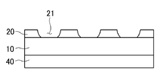
도 3은 본원의 일 구현예에 따른 개구부를 포함하는 마스크층을 이용하여 미세 구조물의 위치 제어를 설명하는 단면도이다.
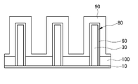
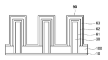
도 4는 본원의 일 구현예에 따른 태양전지의 전하분리 접합부를 나타내는 단면도이다.
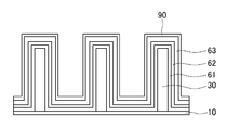
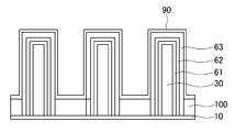
도 5는 본원의 일 구현예에 따른 태양전지의 절연층의 다양한 형태를 보여주는 단면도이다.
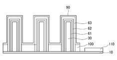
도 6은 본원의 일 구현예에 따른 다양한 위치에 전극이 형성되어 있는 태양전지의 단면도이다.
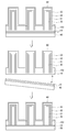
도 7은 본원의 일 구현예에 따른 태양전지의 전사과정을 설명하는 그림이다.
20: 마스크층
21: 개구부
30: 미세 구조물
40: 기판
50: 목적 기판
60: 전하분리층
61: 제 1 전하분리층
62: 제 2 전하분리층
63: 제 3 전하분리층
80: 전하분리접합부
90: 제 1 전극층
100: 절연층
110: 제 2 전극층
Claims (24)
- 탄소구조체층;
상기 탄소구조체층 상에 형성되어 있는 미세 구조물; 및
상기 미세 구조물 표면에 형성되어 있는, 전하분리접합부를 포함하는 전하분리층:
을 포함하는, 태양전지.
- 제 1 항에 있어서,
상기 탄소구조체층 하부에 기판을 추가 포함하는, 태양전지.
- 제 2 항에 있어서,
상기 탄소구조체층과 상기 기판은 분리가능한 것인, 태양전지.
- 제 1 항에 있어서,
상기 탄소구조체층은 그래핀(graphene) 또는 그래파이트(graphite)를 포함하는 것인, 태양전지.
- 제 1 항에 있어서,
상기 전하분리층 상에 형성된 제 1 전극층을 추가 포함하는, 태양전지.
- 제 5 항에 있어서,
상기 탄소구조체층과 상기 제 1 전극층 사이에 위치한 절연층을 추가 포함하는, 태양전지.
- 제 1 항에 있어서,
상기 탄소구조체층의 표면 상에 형성된 제 2 전극층을 추가 포함하는, 태양전지.
- 제 1 항에 있어서,
상기 전하분리층은 한 개 또는 복수개의 층인 것인, 태양전지.
- 제 8 항에 있어서,
상기 전하분리접합부는 상기 미세 구조물과 상기 박막의 계면 및/또는 상기 복수개의 전하분리층의 각각의 계면에 형성되어 있는 것인, 태양전지.
- 제 1 항에 있어서,
상기 미세 구조물은 금속 또는 반도체 중 적어도 어느 하나로 이루어진 것인, 태양전지.
- 제 1 항에 있어서,
상기 미세 구조물은 미세 막대, 미세 바늘, 미세 튜브, 미세 벽 및 이들의 조합으로 이루어진 군에서 선택되는 것을 포함하는 것인, 태양전지.
- 제 1 항에 있어서,
상기 전하분리층은 금속 또는 반도체 중 적어도 어느 하나로 이루어진 것인, 태양전지.
- 제 1 항에 있어서,
상기 미세구조물은 상기 탄소구조체층 상의 데미지(damage) 상측에 형성되어 있는, 태양전지.
- 제 1 항에 있어서,
상기 탄소구조체층은 상기 태양전지의 전극인 것인, 태양전지.
- 탄소구조체층을 준비하는 단계;
상기 탄소구조체층 상에 미세 구조물을 성장시키는 단계; 및
상기 미세 구조물 표면에 전하분리층을 형성하는 단계:
를 포함하는, 태양전지의 제조 방법.
- 제 15 항에 있어서,
상기 전하분리층 상에 제 1 전극층을 형성하는 단계를 추가 포함하는, 태양전지의 제조 방법.
- 제 16 항에 있어서,
상기 전하분리층의 형성 이전 또는 후에 상기 탄소구조체층과 상기 제 1 전극층 사이에 절연층을 형성하는 단계를 추가 포함하는, 태양전지의 제조 방법.
- 제 15 항에 있어서,
상기 탄소구조체층의 표면 상에 제 2 전극층을 형성하는 단계를 추가 포함하는, 태양전지의 제조 방법.
- 제 15 항에 있어서,
상기 탄소구조체층을 준비하는 단계는 기판 상에 상기 탄소구조체층을 형성하는 것인, 태양전지의 제조 방법.
- 제 19 항에 있어서,
상기 기판 상에 형성된 탄소구조체층을 목적 기판 상으로 전사하는 것을 추가 포함하는, 태양전지의 제조 방법.
- 제 15 항에 있어서,
상기 탄소구조체층 상에 미세 구조물을 성장시키는 단계는,
상기 탄소구조체층 상에 데미지를 형성하고, 상기 데미지 상측에 상기 미세 구조물을 형성하는 것인, 태양전지의 제조 방법.
- 제 21 항에 있어서,
상기 데미지는, 가스 플라즈마, 이온빔, 전자빔, 양성자빔, 중성자빔 및 이들의 조합으로 이루어진 군에서 선택되는 방법 중 하나에 의해 형성되는 것인, 태양전지의 제조 방법.
- 제 21 항에 있어서,
상기 데미지를 형성하는 것은,
상기 탄소구조체층 상에 마스크층을 형성하는 단계;
상기 마스크층을 패터닝하여 복수개의 개구부를 형성하는 단계; 및
상기 개구부를 통해 상기 탄소구조체층에 데미지를 생성하는 단계:
를 포함하는 것인, 태양전지의 제조 방법.
- 제 23 항에 있어서,
상기 마스크층을 패터닝하여 복수개의 개구부를 형성하는 단계는 전자빔 리소그래피, 포토리소그래피, 레이저 간섭 리소그래피, 나노임프린트, 및 탬플릿 중 하나 이상의 방법을 이용하는 것인, 태양전지의 제조 방법.
Priority Applications (3)
| Application Number | Priority Date | Filing Date | Title |
|---|---|---|---|
| KR1020100103904A KR101142545B1 (ko) | 2010-10-25 | 2010-10-25 | 태양전지 및 그 제조 방법 |
| US13/881,479 US9419158B2 (en) | 2010-10-25 | 2011-10-25 | Solar cell and method for manufacturing same |
| PCT/KR2011/007993 WO2012057504A2 (ko) | 2010-10-25 | 2011-10-25 | 태양전지 및 그 제조 방법 |
Applications Claiming Priority (1)
| Application Number | Priority Date | Filing Date | Title |
|---|---|---|---|
| KR1020100103904A KR101142545B1 (ko) | 2010-10-25 | 2010-10-25 | 태양전지 및 그 제조 방법 |
Publications (2)
| Publication Number | Publication Date |
|---|---|
| KR20120042282A true KR20120042282A (ko) | 2012-05-03 |
| KR101142545B1 KR101142545B1 (ko) | 2012-05-08 |
Family
ID=45994543
Family Applications (1)
| Application Number | Title | Priority Date | Filing Date |
|---|---|---|---|
| KR1020100103904A Active KR101142545B1 (ko) | 2010-10-25 | 2010-10-25 | 태양전지 및 그 제조 방법 |
Country Status (3)
| Country | Link |
|---|---|
| US (1) | US9419158B2 (ko) |
| KR (1) | KR101142545B1 (ko) |
| WO (1) | WO2012057504A2 (ko) |
Cited By (4)
| Publication number | Priority date | Publication date | Assignee | Title |
|---|---|---|---|---|
| KR101405557B1 (ko) * | 2012-12-21 | 2014-06-11 | 경희대학교 산학협력단 | 그래핀 태양전지 |
| KR20150048705A (ko) * | 2012-06-21 | 2015-05-07 | 노르웨이전 유니버시티 오브 사이언스 앤드 테크놀러지(엔티엔유) | 태양전지 |
| KR101519703B1 (ko) * | 2012-11-20 | 2015-05-21 | 현대자동차주식회사 | 태양전지 및 이의 제조방법 |
| KR20160061997A (ko) * | 2013-08-14 | 2016-06-01 | 노르웨이전 유니버시티 오브 사이언스 앤드 테크놀러지(엔티엔유) | 레이디얼 p-n 접합 나노와이어 태양전지 |
Families Citing this family (10)
| Publication number | Priority date | Publication date | Assignee | Title |
|---|---|---|---|---|
| GB201021112D0 (en) | 2010-12-13 | 2011-01-26 | Ntnu Technology Transfer As | Nanowires |
| GB201200355D0 (en) | 2012-01-10 | 2012-02-22 | Norwegian Univ Sci & Tech Ntnu | Nanowires |
| GB201311101D0 (en) | 2013-06-21 | 2013-08-07 | Norwegian Univ Sci & Tech Ntnu | Semiconducting Films |
| KR101515301B1 (ko) | 2013-09-17 | 2015-04-27 | 전남대학교산학협력단 | 레이저 리소그래피를 이용하여 형성되는 3차원 구조의 광흡수층을 가지는 태양전지 제조방법 |
| US10347791B2 (en) | 2015-07-13 | 2019-07-09 | Crayonano As | Nanowires or nanopyramids grown on graphitic substrate |
| CN108292694A (zh) * | 2015-07-13 | 2018-07-17 | 科莱约纳诺公司 | 纳米线/纳米锥形状的发光二极管及光检测器 |
| EA201890238A1 (ru) | 2015-07-31 | 2018-08-31 | Крайонано Ас | Способ выращивания нанопроволок или нанопирамидок на графитовых подложках |
| GB201705755D0 (en) | 2017-04-10 | 2017-05-24 | Norwegian Univ Of Science And Tech (Ntnu) | Nanostructure |
| GB201913701D0 (en) | 2019-09-23 | 2019-11-06 | Crayonano As | Composition of matter |
| CN111952458A (zh) * | 2020-08-24 | 2020-11-17 | 中国科学院半导体研究所 | 曲面异质结太阳电池及其制作方法 |
Family Cites Families (9)
| Publication number | Priority date | Publication date | Assignee | Title |
|---|---|---|---|---|
| JP2007027625A (ja) * | 2005-07-21 | 2007-02-01 | Matsushita Electric Works Ltd | 有機太陽電池及びその製造方法 |
| JP4720426B2 (ja) * | 2005-10-19 | 2011-07-13 | 住友金属鉱山株式会社 | カーボンナノチューブを用いた太陽電池 |
| US20080110486A1 (en) * | 2006-11-15 | 2008-05-15 | General Electric Company | Amorphous-crystalline tandem nanostructured solar cells |
| KR20080081605A (ko) * | 2007-03-06 | 2008-09-10 | 삼성전자주식회사 | 절연 모기판에 얼라인 마크를 형성하는 단계를 포함하는액정 표시 장치의 제조 방법 |
| KR100809248B1 (ko) | 2007-03-14 | 2008-02-29 | 삼성전기주식회사 | 반도체 이종구조 나노선을 이용한 광기전력 소자 및 그제조방법 |
| US20100012190A1 (en) * | 2008-07-16 | 2010-01-21 | Hajime Goto | Nanowire photovoltaic cells and manufacture method thereof |
| JP2010028092A (ja) | 2008-07-16 | 2010-02-04 | Honda Motor Co Ltd | ナノワイヤ太陽電池及びその製造方法 |
| KR101040956B1 (ko) * | 2009-02-26 | 2011-06-16 | 전자부품연구원 | 산화아연 나노와이어를 이용한 박막 실리콘 태양전지 및 그의 제조방법 |
| US10164135B2 (en) * | 2009-08-07 | 2018-12-25 | Guardian Glass, LLC | Electronic device including graphene-based layer(s), and/or method or making the same |
-
2010
- 2010-10-25 KR KR1020100103904A patent/KR101142545B1/ko active Active
-
2011
- 2011-10-25 WO PCT/KR2011/007993 patent/WO2012057504A2/ko not_active Ceased
- 2011-10-25 US US13/881,479 patent/US9419158B2/en active Active
Cited By (6)
| Publication number | Priority date | Publication date | Assignee | Title |
|---|---|---|---|---|
| KR20150048705A (ko) * | 2012-06-21 | 2015-05-07 | 노르웨이전 유니버시티 오브 사이언스 앤드 테크놀러지(엔티엔유) | 태양전지 |
| JP2015528202A (ja) * | 2012-06-21 | 2015-09-24 | ノルウェージャン ユニバーシティ オブ サイエンス アンド テクノロジー(エヌティーエヌユー) | 太陽電池 |
| EP2865009B1 (en) * | 2012-06-21 | 2023-08-02 | Norwegian University of Science and Technology (NTNU) | Solar cells |
| KR101519703B1 (ko) * | 2012-11-20 | 2015-05-21 | 현대자동차주식회사 | 태양전지 및 이의 제조방법 |
| KR101405557B1 (ko) * | 2012-12-21 | 2014-06-11 | 경희대학교 산학협력단 | 그래핀 태양전지 |
| KR20160061997A (ko) * | 2013-08-14 | 2016-06-01 | 노르웨이전 유니버시티 오브 사이언스 앤드 테크놀러지(엔티엔유) | 레이디얼 p-n 접합 나노와이어 태양전지 |
Also Published As
| Publication number | Publication date |
|---|---|
| US20130213470A1 (en) | 2013-08-22 |
| WO2012057504A2 (ko) | 2012-05-03 |
| US9419158B2 (en) | 2016-08-16 |
| KR101142545B1 (ko) | 2012-05-08 |
| WO2012057504A3 (ko) | 2012-07-26 |
Similar Documents
| Publication | Publication Date | Title |
|---|---|---|
| KR101142545B1 (ko) | 태양전지 및 그 제조 방법 | |
| JP6343608B2 (ja) | 太陽電池 | |
| JP6959915B2 (ja) | グラファイト基板上に成長させたナノワイヤ又はナノピラミッド | |
| CN102782864B (zh) | 多结化合物半导体太阳能电池 | |
| US8747942B2 (en) | Carbon nanotube-based solar cells | |
| US20120006390A1 (en) | Nano-wire solar cell or detector | |
| US20080006319A1 (en) | Photovoltaic and photosensing devices based on arrays of aligned nanostructures | |
| CN111725338B (zh) | 一种微米线阵列异质结紫外光探测器及其制备方法 | |
| US20090217972A1 (en) | Techniques for Enhancing Efficiency of Photovoltaic Devices Using High-Aspect-Ratio Nanostructures | |
| EP2253021B1 (en) | Photovoltaic devices with high-aspect-ratio nanostructures | |
| KR101100414B1 (ko) | 태양전지 및 그 제조 방법 | |
| CN105304737B (zh) | 一种可控阵列纳米线太阳能电池及其制备方法 | |
| US20150000730A1 (en) | Method for the low-temperature production of radial-junction semiconductor nanostructures, radial junction device, and solar cell including radial-junction nanostructures | |
| JP5758257B2 (ja) | 化合物半導体太陽電池製造用積層体、化合物半導体太陽電池およびその製造方法 | |
| Kohen et al. | Enhanced photovoltaic performance of vapor–liquid–solid grown silicon nanowire array with radial heterojunction | |
| KR101772694B1 (ko) | 나노구조체의 제조방법 및 이를 이용한 전자소자의 제조방법 | |
| CN102723404A (zh) | 倒置生长宽谱吸收iii-v多结电池的制备方法 | |
| Atwater | Tandem Microwire Solar Cells for Flexible High Efficiency Low Cost Photovoltaics | |
| Wang et al. | Three-Dimensional Photovoltaic Devices Based on Vertically Aligned Nanowire Array |
Legal Events
| Date | Code | Title | Description |
|---|---|---|---|
| A201 | Request for examination | ||
| PA0109 | Patent application |
St.27 status event code: A-0-1-A10-A12-nap-PA0109 |
|
| PA0201 | Request for examination |
St.27 status event code: A-1-2-D10-D11-exm-PA0201 |
|
| D13-X000 | Search requested |
St.27 status event code: A-1-2-D10-D13-srh-X000 |
|
| PN2301 | Change of applicant |
St.27 status event code: A-3-3-R10-R13-asn-PN2301 St.27 status event code: A-3-3-R10-R11-asn-PN2301 |
|
| R17-X000 | Change to representative recorded |
St.27 status event code: A-3-3-R10-R17-oth-X000 |
|
| R17-X000 | Change to representative recorded |
St.27 status event code: A-3-3-R10-R17-oth-X000 |
|
| D14-X000 | Search report completed |
St.27 status event code: A-1-2-D10-D14-srh-X000 |
|
| E902 | Notification of reason for refusal | ||
| PE0902 | Notice of grounds for rejection |
St.27 status event code: A-1-2-D10-D21-exm-PE0902 |
|
| P11-X000 | Amendment of application requested |
St.27 status event code: A-2-2-P10-P11-nap-X000 |
|
| P13-X000 | Application amended |
St.27 status event code: A-2-2-P10-P13-nap-X000 |
|
| E701 | Decision to grant or registration of patent right | ||
| PE0701 | Decision of registration |
St.27 status event code: A-1-2-D10-D22-exm-PE0701 |
|
| GRNT | Written decision to grant | ||
| PR0701 | Registration of establishment |
St.27 status event code: A-2-4-F10-F11-exm-PR0701 |
|
| PR1002 | Payment of registration fee |
St.27 status event code: A-2-2-U10-U11-oth-PR1002 Fee payment year number: 1 |
|
| PG1501 | Laying open of application |
St.27 status event code: A-1-1-Q10-Q12-nap-PG1501 |
|
| PG1601 | Publication of registration |
St.27 status event code: A-4-4-Q10-Q13-nap-PG1601 |
|
| R18-X000 | Changes to party contact information recorded |
St.27 status event code: A-5-5-R10-R18-oth-X000 |
|
| P22-X000 | Classification modified |
St.27 status event code: A-4-4-P10-P22-nap-X000 |
|
| FPAY | Annual fee payment |
Payment date: 20150226 Year of fee payment: 4 |
|
| PR1001 | Payment of annual fee |
St.27 status event code: A-4-4-U10-U11-oth-PR1001 Fee payment year number: 4 |
|
| PN2301 | Change of applicant |
St.27 status event code: A-5-5-R10-R13-asn-PN2301 St.27 status event code: A-5-5-R10-R11-asn-PN2301 |
|
| PN2301 | Change of applicant |
St.27 status event code: A-5-5-R10-R13-asn-PN2301 St.27 status event code: A-5-5-R10-R11-asn-PN2301 |
|
| FPAY | Annual fee payment |
Payment date: 20160128 Year of fee payment: 5 |
|
| PR1001 | Payment of annual fee |
St.27 status event code: A-4-4-U10-U11-oth-PR1001 Fee payment year number: 5 |
|
| FPAY | Annual fee payment |
Payment date: 20170403 Year of fee payment: 6 |
|
| PR1001 | Payment of annual fee |
St.27 status event code: A-4-4-U10-U11-oth-PR1001 Fee payment year number: 6 |
|
| PR1001 | Payment of annual fee |
St.27 status event code: A-4-4-U10-U11-oth-PR1001 Fee payment year number: 7 |
|
| FPAY | Annual fee payment |
Payment date: 20190508 Year of fee payment: 8 |
|
| PR1001 | Payment of annual fee |
St.27 status event code: A-4-4-U10-U11-oth-PR1001 Fee payment year number: 8 |
|
| R18-X000 | Changes to party contact information recorded |
St.27 status event code: A-5-5-R10-R18-oth-X000 |
|
| R18-X000 | Changes to party contact information recorded |
St.27 status event code: A-5-5-R10-R18-oth-X000 |
|
| PN2301 | Change of applicant |
St.27 status event code: A-5-5-R10-R13-asn-PN2301 St.27 status event code: A-5-5-R10-R11-asn-PN2301 |
|
| PR1001 | Payment of annual fee |
St.27 status event code: A-4-4-U10-U11-oth-PR1001 Fee payment year number: 9 |
|
| PN2301 | Change of applicant |
St.27 status event code: A-5-5-R10-R13-asn-PN2301 St.27 status event code: A-5-5-R10-R11-asn-PN2301 |
|
| PR1001 | Payment of annual fee |
St.27 status event code: A-4-4-U10-U11-oth-PR1001 Fee payment year number: 10 |
|
| R18-X000 | Changes to party contact information recorded |
St.27 status event code: A-5-5-R10-R18-oth-X000 |
|
| R18-X000 | Changes to party contact information recorded |
St.27 status event code: A-5-5-R10-R18-oth-X000 |
|
| R18-X000 | Changes to party contact information recorded |
St.27 status event code: A-5-5-R10-R18-oth-X000 |
|
| R18-X000 | Changes to party contact information recorded |
St.27 status event code: A-5-5-R10-R18-oth-X000 |
|
| R18-X000 | Changes to party contact information recorded |
St.27 status event code: A-5-5-R10-R18-oth-X000 |
|
| P22-X000 | Classification modified |
St.27 status event code: A-4-4-P10-P22-nap-X000 |
|
| PR1001 | Payment of annual fee |
St.27 status event code: A-4-4-U10-U11-oth-PR1001 Fee payment year number: 14 |
|
| R18-X000 | Changes to party contact information recorded |
St.27 status event code: A-5-5-R10-R18-oth-X000 |
|
| R18 | Changes to party contact information recorded |
Free format text: ST27 STATUS EVENT CODE: A-5-5-R10-R18-OTH-X000 (AS PROVIDED BY THE NATIONAL OFFICE) |
|
| R18-X000 | Changes to party contact information recorded |
St.27 status event code: A-5-5-R10-R18-oth-X000 |
|
| PR1001 | Payment of annual fee |
St.27 status event code: A-4-4-U10-U11-oth-PR1001 Fee payment year number: 15 |
|
| U11 | Full renewal or maintenance fee paid |
Free format text: ST27 STATUS EVENT CODE: A-4-4-U10-U11-OTH-PR1001 (AS PROVIDED BY THE NATIONAL OFFICE) Year of fee payment: 15 |