KR20120048020A - 형광체, 발광 장치, 및 그를 사용한 액정 표시 장치 - Google Patents
형광체, 발광 장치, 및 그를 사용한 액정 표시 장치 Download PDFInfo
- Publication number
- KR20120048020A KR20120048020A KR1020127006888A KR20127006888A KR20120048020A KR 20120048020 A KR20120048020 A KR 20120048020A KR 1020127006888 A KR1020127006888 A KR 1020127006888A KR 20127006888 A KR20127006888 A KR 20127006888A KR 20120048020 A KR20120048020 A KR 20120048020A
- Authority
- KR
- South Korea
- Prior art keywords
- light emitting
- light
- phosphor
- emitting device
- general formula
- Prior art date
- Legal status (The legal status is an assumption and is not a legal conclusion. Google has not performed a legal analysis and makes no representation as to the accuracy of the status listed.)
- Granted
Links
Images

Classifications
-
- C—CHEMISTRY; METALLURGY
- C09—DYES; PAINTS; POLISHES; NATURAL RESINS; ADHESIVES; COMPOSITIONS NOT OTHERWISE PROVIDED FOR; APPLICATIONS OF MATERIALS NOT OTHERWISE PROVIDED FOR
- C09K—MATERIALS FOR MISCELLANEOUS APPLICATIONS, NOT PROVIDED FOR ELSEWHERE
- C09K11/00—Luminescent materials, e.g. electroluminescent or chemiluminescent
- C09K11/08—Luminescent materials, e.g. electroluminescent or chemiluminescent containing inorganic luminescent materials
- C09K11/64—Luminescent materials, e.g. electroluminescent or chemiluminescent containing inorganic luminescent materials containing aluminium
-
- H—ELECTRICITY
- H10—SEMICONDUCTOR DEVICES; ELECTRIC SOLID-STATE DEVICES NOT OTHERWISE PROVIDED FOR
- H10H—INORGANIC LIGHT-EMITTING SEMICONDUCTOR DEVICES HAVING POTENTIAL BARRIERS
- H10H20/00—Individual inorganic light-emitting semiconductor devices having potential barriers, e.g. light-emitting diodes [LED]
- H10H20/80—Constructional details
- H10H20/85—Packages
- H10H20/851—Wavelength conversion means
- H10H20/8511—Wavelength conversion means characterised by their material, e.g. binder
- H10H20/8512—Wavelength conversion materials
- H10H20/8513—Wavelength conversion materials having two or more wavelength conversion materials
-
- C—CHEMISTRY; METALLURGY
- C09—DYES; PAINTS; POLISHES; NATURAL RESINS; ADHESIVES; COMPOSITIONS NOT OTHERWISE PROVIDED FOR; APPLICATIONS OF MATERIALS NOT OTHERWISE PROVIDED FOR
- C09K—MATERIALS FOR MISCELLANEOUS APPLICATIONS, NOT PROVIDED FOR ELSEWHERE
- C09K11/00—Luminescent materials, e.g. electroluminescent or chemiluminescent
- C09K11/08—Luminescent materials, e.g. electroluminescent or chemiluminescent containing inorganic luminescent materials
- C09K11/0883—Arsenides; Nitrides; Phosphides
-
- C—CHEMISTRY; METALLURGY
- C09—DYES; PAINTS; POLISHES; NATURAL RESINS; ADHESIVES; COMPOSITIONS NOT OTHERWISE PROVIDED FOR; APPLICATIONS OF MATERIALS NOT OTHERWISE PROVIDED FOR
- C09K—MATERIALS FOR MISCELLANEOUS APPLICATIONS, NOT PROVIDED FOR ELSEWHERE
- C09K11/00—Luminescent materials, e.g. electroluminescent or chemiluminescent
- C09K11/08—Luminescent materials, e.g. electroluminescent or chemiluminescent containing inorganic luminescent materials
- C09K11/59—Luminescent materials, e.g. electroluminescent or chemiluminescent containing inorganic luminescent materials containing silicon
-
- C—CHEMISTRY; METALLURGY
- C09—DYES; PAINTS; POLISHES; NATURAL RESINS; ADHESIVES; COMPOSITIONS NOT OTHERWISE PROVIDED FOR; APPLICATIONS OF MATERIALS NOT OTHERWISE PROVIDED FOR
- C09K—MATERIALS FOR MISCELLANEOUS APPLICATIONS, NOT PROVIDED FOR ELSEWHERE
- C09K11/00—Luminescent materials, e.g. electroluminescent or chemiluminescent
- C09K11/08—Luminescent materials, e.g. electroluminescent or chemiluminescent containing inorganic luminescent materials
- C09K11/77—Luminescent materials, e.g. electroluminescent or chemiluminescent containing inorganic luminescent materials containing rare earth metals
-
- C—CHEMISTRY; METALLURGY
- C09—DYES; PAINTS; POLISHES; NATURAL RESINS; ADHESIVES; COMPOSITIONS NOT OTHERWISE PROVIDED FOR; APPLICATIONS OF MATERIALS NOT OTHERWISE PROVIDED FOR
- C09K—MATERIALS FOR MISCELLANEOUS APPLICATIONS, NOT PROVIDED FOR ELSEWHERE
- C09K11/00—Luminescent materials, e.g. electroluminescent or chemiluminescent
- C09K11/08—Luminescent materials, e.g. electroluminescent or chemiluminescent containing inorganic luminescent materials
- C09K11/77—Luminescent materials, e.g. electroluminescent or chemiluminescent containing inorganic luminescent materials containing rare earth metals
- C09K11/7728—Luminescent materials, e.g. electroluminescent or chemiluminescent containing inorganic luminescent materials containing rare earth metals containing europium
- C09K11/77348—Silicon Aluminium Nitrides or Silicon Aluminium Oxynitrides
-
- G—PHYSICS
- G02—OPTICS
- G02F—OPTICAL DEVICES OR ARRANGEMENTS FOR THE CONTROL OF LIGHT BY MODIFICATION OF THE OPTICAL PROPERTIES OF THE MEDIA OF THE ELEMENTS INVOLVED THEREIN; NON-LINEAR OPTICS; FREQUENCY-CHANGING OF LIGHT; OPTICAL LOGIC ELEMENTS; OPTICAL ANALOGUE/DIGITAL CONVERTERS
- G02F1/00—Devices or arrangements for the control of the intensity, colour, phase, polarisation or direction of light arriving from an independent light source, e.g. switching, gating or modulating; Non-linear optics
- G02F1/01—Devices or arrangements for the control of the intensity, colour, phase, polarisation or direction of light arriving from an independent light source, e.g. switching, gating or modulating; Non-linear optics for the control of the intensity, phase, polarisation or colour
- G02F1/13—Devices or arrangements for the control of the intensity, colour, phase, polarisation or direction of light arriving from an independent light source, e.g. switching, gating or modulating; Non-linear optics for the control of the intensity, phase, polarisation or colour based on liquid crystals, e.g. single liquid crystal display cells
- G02F1/133—Constructional arrangements; Operation of liquid crystal cells; Circuit arrangements
- G02F1/1333—Constructional arrangements; Manufacturing methods
- G02F1/1335—Structural association of cells with optical devices, e.g. polarisers or reflectors
-
- G—PHYSICS
- G02—OPTICS
- G02F—OPTICAL DEVICES OR ARRANGEMENTS FOR THE CONTROL OF LIGHT BY MODIFICATION OF THE OPTICAL PROPERTIES OF THE MEDIA OF THE ELEMENTS INVOLVED THEREIN; NON-LINEAR OPTICS; FREQUENCY-CHANGING OF LIGHT; OPTICAL LOGIC ELEMENTS; OPTICAL ANALOGUE/DIGITAL CONVERTERS
- G02F1/00—Devices or arrangements for the control of the intensity, colour, phase, polarisation or direction of light arriving from an independent light source, e.g. switching, gating or modulating; Non-linear optics
- G02F1/01—Devices or arrangements for the control of the intensity, colour, phase, polarisation or direction of light arriving from an independent light source, e.g. switching, gating or modulating; Non-linear optics for the control of the intensity, phase, polarisation or colour
- G02F1/13—Devices or arrangements for the control of the intensity, colour, phase, polarisation or direction of light arriving from an independent light source, e.g. switching, gating or modulating; Non-linear optics for the control of the intensity, phase, polarisation or colour based on liquid crystals, e.g. single liquid crystal display cells
- G02F1/133—Constructional arrangements; Operation of liquid crystal cells; Circuit arrangements
- G02F1/1333—Constructional arrangements; Manufacturing methods
- G02F1/1335—Structural association of cells with optical devices, e.g. polarisers or reflectors
- G02F1/1336—Illuminating devices
-
- G—PHYSICS
- G02—OPTICS
- G02F—OPTICAL DEVICES OR ARRANGEMENTS FOR THE CONTROL OF LIGHT BY MODIFICATION OF THE OPTICAL PROPERTIES OF THE MEDIA OF THE ELEMENTS INVOLVED THEREIN; NON-LINEAR OPTICS; FREQUENCY-CHANGING OF LIGHT; OPTICAL LOGIC ELEMENTS; OPTICAL ANALOGUE/DIGITAL CONVERTERS
- G02F1/00—Devices or arrangements for the control of the intensity, colour, phase, polarisation or direction of light arriving from an independent light source, e.g. switching, gating or modulating; Non-linear optics
- G02F1/01—Devices or arrangements for the control of the intensity, colour, phase, polarisation or direction of light arriving from an independent light source, e.g. switching, gating or modulating; Non-linear optics for the control of the intensity, phase, polarisation or colour
- G02F1/13—Devices or arrangements for the control of the intensity, colour, phase, polarisation or direction of light arriving from an independent light source, e.g. switching, gating or modulating; Non-linear optics for the control of the intensity, phase, polarisation or colour based on liquid crystals, e.g. single liquid crystal display cells
- G02F1/133—Constructional arrangements; Operation of liquid crystal cells; Circuit arrangements
- G02F1/1333—Constructional arrangements; Manufacturing methods
- G02F1/1335—Structural association of cells with optical devices, e.g. polarisers or reflectors
- G02F1/1336—Illuminating devices
- G02F1/133602—Direct backlight
- G02F1/133603—Direct backlight with LEDs
-
- H—ELECTRICITY
- H10—SEMICONDUCTOR DEVICES; ELECTRIC SOLID-STATE DEVICES NOT OTHERWISE PROVIDED FOR
- H10H—INORGANIC LIGHT-EMITTING SEMICONDUCTOR DEVICES HAVING POTENTIAL BARRIERS
- H10H20/00—Individual inorganic light-emitting semiconductor devices having potential barriers, e.g. light-emitting diodes [LED]
- H10H20/80—Constructional details
- H10H20/85—Packages
- H10H20/851—Wavelength conversion means
- H10H20/8511—Wavelength conversion means characterised by their material, e.g. binder
- H10H20/8512—Wavelength conversion materials
-
- H—ELECTRICITY
- H10—SEMICONDUCTOR DEVICES; ELECTRIC SOLID-STATE DEVICES NOT OTHERWISE PROVIDED FOR
- H10W—GENERIC PACKAGES, INTERCONNECTIONS, CONNECTORS OR OTHER CONSTRUCTIONAL DETAILS OF DEVICES COVERED BY CLASS H10
- H10W90/00—Package configurations
- H10W90/701—Package configurations characterised by the relative positions of pads or connectors relative to package parts
- H10W90/751—Package configurations characterised by the relative positions of pads or connectors relative to package parts of bond wires
- H10W90/756—Package configurations characterised by the relative positions of pads or connectors relative to package parts of bond wires between a chip and a stacked lead frame, conducting package substrate or heat sink
-
- Y—GENERAL TAGGING OF NEW TECHNOLOGICAL DEVELOPMENTS; GENERAL TAGGING OF CROSS-SECTIONAL TECHNOLOGIES SPANNING OVER SEVERAL SECTIONS OF THE IPC; TECHNICAL SUBJECTS COVERED BY FORMER USPC CROSS-REFERENCE ART COLLECTIONS [XRACs] AND DIGESTS
- Y10—TECHNICAL SUBJECTS COVERED BY FORMER USPC
- Y10T—TECHNICAL SUBJECTS COVERED BY FORMER US CLASSIFICATION
- Y10T428/00—Stock material or miscellaneous articles
- Y10T428/29—Coated or structually defined flake, particle, cell, strand, strand portion, rod, filament, macroscopic fiber or mass thereof
- Y10T428/2982—Particulate matter [e.g., sphere, flake, etc.]
Landscapes
- Chemical & Material Sciences (AREA)
- Physics & Mathematics (AREA)
- Inorganic Chemistry (AREA)
- Engineering & Computer Science (AREA)
- Materials Engineering (AREA)
- Organic Chemistry (AREA)
- Nonlinear Science (AREA)
- Mathematical Physics (AREA)
- Crystallography & Structural Chemistry (AREA)
- General Physics & Mathematics (AREA)
- Optics & Photonics (AREA)
- Luminescent Compositions (AREA)
- Led Device Packages (AREA)
- Liquid Crystal (AREA)
- Devices For Indicating Variable Information By Combining Individual Elements (AREA)
Abstract
Description
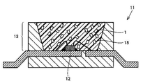
도 2는 본 발명의 다른 바람직한 일례의 발광 장치(21)를 대략적으로 나타낸 단면도이다.
|
|
초기 | 5000시간 후 |
| 밝기(상대값) | 밝기(유지율) | |
| 실시예 1 | 109.8% | 90.3% |
| 비교예 1 | 100.0% | 70.6% |
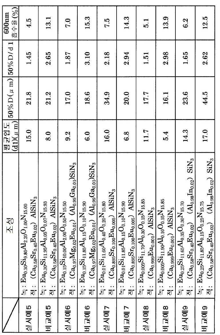
| 조성 | 평균입도 (d1)(μm) |
50% D (μm) |
50% D/d1 | 600nm 흡수율(%) |
|
| 실시예 2 | Eu0.05Si11.50Al0.50O0.30N15.70 | 13.1 | 21.0 | 1.60 | 6.30 |
| 비교예 2 | Eu0.05Si11.95Al0.05O0.06N15.94 | 7.3 | 17.5 | 2.40 | 13.6 |
| 실시예 3 | Eu0.10Si11.00Al1.00O0.40N15.60 | 9.5 | 15.0 | 1.58 | 5.70 |
| 비교예 3 | Eu0.10Si11.90Al0.10O0.10N15.90 | 5.9 | 16.8 | 2.85 | 14.7 |
|
|
초기 | 5000시간 후 |
| 밝기(상대값) | 밝기(유지율) | |
| 실시예 2 | 110.8% | 91.6% |
| 비교예 2 | 100.0% | 72.1% |
| 실시예 3 | 109.0% | 90.9% |
| 비교예 3 | 100.0% | 71.3% |
|
|
초기 | 5000시간 후 | ||||
| 밝기 (상대값) |
x | y | 밝기 (유지율) |
x | y | |
| 실시예 4 | 108.5% | 0.295 | 0.280 | 92.5% | 0.294 | 0.278 |
| 비교예 4 | 100.0% | 0.296 | 0.280 | 74.8% | 0.290 | 0.268 |

11,21 : 발광 장치
12 : 발광 소자
13 : 파장 변환부
14 : 본 발명의 형광체 이외의 형광체
15 : 매질
Claims (12)
- 일반식 (A) : EuaSibAlcOdNe
(일반식 (A) 중 0.005≤a≤0.4, b+c=12, d+e=16을 만족하는 수이다.)로 실질적으로 표시되고, 평균 입도(d1)(공기 투과법)가 9~16μm이고, 입도 분포에서의 메디안 직경 (50% D)이 12.5~35μm이고, 50% D/d1=1.4~2.2이고, 또한 600nm에 있어서의 흡수율이 8.0% 이하인 β형 SiAlON인, 2가의 유로퓸 활성화 산질화물 녹색계 발광 형광체. - 제1항에 있어서, 10μm≤d1≤13μm, 50% D/d1=1.6~2.0이고 600nm에 있어서의 흡수율이 7.0% 이하인, 형광체.
- 제1항에 있어서, 일반식 (A) 중, c≥0.3인, 형광체.
- 제1항에 있어서, 일반식 (A) 중, 0.01≤a≤0.2인, 형광체.
- 피크 파장이 430~480nm의 1차광을 발하는 질화갈륨계 반도체인 발광 소자와, 상기 1차광의 일부를 흡수하여 1차광의 파장보다도 긴 파장을 갖는 2차광을 발하는 파장 변환부를 구비한 발광 장치로서, 상기 파장 변환부는,
일반식 (A) : EuaSibAlcOdNe
(일반식 (A) 중 0.005≤a≤0.4, b+c=12, d+e=16을 만족하는 수이다.)로 실질적으로 표시되고, 평균 입도(d1) (공기 투과법)가 9~16μm이고, 입도 분포에서의 메디안 직경(50% D)이 12.5~35μm이고, 50% D/d1=1.4~2.2이고, 또한 600nm에 있어서의 흡수율이 8.0% 이하인 β형 SiAlON인, 2가의 유로퓸 활성화 산질화물 녹색계 발광 형광체를 포함하는, 발광 장치. - 제5항에 있어서, 형광체가, 10μm≤d1≤13μm, 50% D/d1=1.6~2.0이고 600nm에 있어서의 흡수율이 7.0% 이하인, 발광 장치.
- 제5항에 있어서, 일반식 (A) 중, c≥0.3인, 발광 장치.
- 제5항에 있어서, 일반식 (A) 중, 0.01≤a≤0.2인, 발광 장치.
- 제5항에 있어서,
일반식 (B) : (MI1-xEux) MIISiN3
(일반식 (B) 중 MI는 Mg, Ca, Sr 및 Ba로부터 선택되는 적어도 1종의 알칼리 토류 금속 원소를 나타내며, MII는 Al, Ga, In, Sc, Y, La, Gd 및 Lu로부터 선택되는 적어도 1종의 3가의 금속 원소를 나타내고, 0.001≤x≤0.10을 만족하는 수이다.)로 실질적으로 표시되는 2가의 유로퓸 활성화 질화물 적색계 발광 형광체를 파장 변환부에 포함하는, 발광 장치. - 제5항에 있어서, 일반식 (B) 중, MII는 Al, Ga 및 In으로부터 선택되는 적어도 1종의 원소인, 발광 장치.
- 제5항에 기재된 발광 장치를 점광원으로서 복수 포함하는 백라이트 광원 장치.
- 액정 패널과,
액정 패널의 배면에 배치된 제11항에 기재된 백라이트 광원 장치를 구비하는, 액정 표시 장치.
Applications Claiming Priority (3)
| Application Number | Priority Date | Filing Date | Title |
|---|---|---|---|
| JPJP-P-2010-003058 | 2010-01-08 | ||
| JP2010003058 | 2010-01-08 | ||
| PCT/JP2010/072684 WO2011083671A1 (ja) | 2010-01-08 | 2010-12-16 | 蛍光体、発光装置およびそれを用いた液晶表示装置 |
Publications (2)
| Publication Number | Publication Date |
|---|---|
| KR20120048020A true KR20120048020A (ko) | 2012-05-14 |
| KR101378813B1 KR101378813B1 (ko) | 2014-03-27 |
Family
ID=44305408
Family Applications (1)
| Application Number | Title | Priority Date | Filing Date |
|---|---|---|---|
| KR1020127006888A Active KR101378813B1 (ko) | 2010-01-08 | 2010-12-16 | 형광체, 발광 장치, 및 그를 사용한 액정 표시 장치 |
Country Status (8)
| Country | Link |
|---|---|
| US (2) | US8709283B2 (ko) |
| EP (1) | EP2468836A4 (ko) |
| JP (2) | JP5589002B2 (ko) |
| KR (1) | KR101378813B1 (ko) |
| CN (1) | CN102656248B (ko) |
| BR (1) | BR112012016731A2 (ko) |
| TW (1) | TWI468495B (ko) |
| WO (1) | WO2011083671A1 (ko) |
Cited By (3)
| Publication number | Priority date | Publication date | Assignee | Title |
|---|---|---|---|---|
| JP2013163720A (ja) * | 2012-02-09 | 2013-08-22 | Denki Kagaku Kogyo Kk | 蛍光体及び発光装置 |
| JP2013163721A (ja) * | 2012-02-09 | 2013-08-22 | Denki Kagaku Kogyo Kk | 蛍光体及び発光装置 |
| JP2013163738A (ja) * | 2012-02-09 | 2013-08-22 | Denki Kagaku Kogyo Kk | 蛍光体及び発光装置 |
Families Citing this family (8)
| Publication number | Priority date | Publication date | Assignee | Title |
|---|---|---|---|---|
| JP5367218B2 (ja) | 2006-11-24 | 2013-12-11 | シャープ株式会社 | 蛍光体の製造方法および発光装置の製造方法 |
| CN102790164B (zh) | 2008-03-03 | 2016-08-10 | Ge磷光体技术有限责任公司 | 发光装置 |
| CN102656248B (zh) * | 2010-01-08 | 2014-07-16 | 夏普株式会社 | 荧光体、发光装置及使用它的液晶显示装置 |
| US9399731B2 (en) * | 2012-12-14 | 2016-07-26 | Denka Company Limited | Phosphor, method for producing the same, and luminescent device using the same |
| KR102353443B1 (ko) | 2014-12-22 | 2022-01-21 | 삼성전자주식회사 | 산질화물계 형광체 및 이를 포함하는 백색 발광 장치 |
| WO2017122800A1 (ja) * | 2016-01-15 | 2017-07-20 | デンカ株式会社 | 蛍光体および発光装置 |
| CA3072755C (en) * | 2017-08-18 | 2024-04-30 | Thorlabs, Inc. | Broadband light source based on crystalline phosphor |
| US11781064B2 (en) | 2019-04-23 | 2023-10-10 | Denka Company Limited | Phosphor powder and light-emitting device |
Family Cites Families (24)
| Publication number | Priority date | Publication date | Assignee | Title |
|---|---|---|---|---|
| TW383508B (en) | 1996-07-29 | 2000-03-01 | Nichia Kagaku Kogyo Kk | Light emitting device and display |
| US6608332B2 (en) | 1996-07-29 | 2003-08-19 | Nichia Kagaku Kogyo Kabushiki Kaisha | Light emitting device and display |
| JP3609709B2 (ja) | 2000-09-29 | 2005-01-12 | 株式会社シチズン電子 | 発光ダイオード |
| CA2489237A1 (en) | 2002-06-13 | 2003-12-24 | Cree, Inc. | Semiconductor emitter comprising a saturated phosphor |
| KR100609830B1 (ko) | 2003-04-25 | 2006-08-09 | 럭스피아 주식회사 | 녹색 및 적색형광체를 이용하는 백색 반도체 발광장치 |
| JP3921545B2 (ja) * | 2004-03-12 | 2007-05-30 | 独立行政法人物質・材料研究機構 | 蛍光体とその製造方法 |
| JP4517783B2 (ja) | 2004-08-31 | 2010-08-04 | 日亜化学工業株式会社 | 希土類硼アルミン酸塩蛍光体及びそれを用いた発光装置 |
| KR100880757B1 (ko) | 2004-09-22 | 2009-02-02 | 가부시끼가이샤 도시바 | 발광 장치와 그것을 이용한 백 라이트 및 액정 표시 장치 |
| JP4934792B2 (ja) * | 2005-08-04 | 2012-05-16 | Dowaエレクトロニクス株式会社 | 蛍光体及びその製造方法、並びに当該蛍光体を用いた発光装置 |
| EP2463354B1 (en) | 2005-12-08 | 2017-03-29 | National Institute for Materials Science | Phosphor, Process for producing the same, and luminescent device |
| TW200801158A (en) | 2006-02-02 | 2008-01-01 | Mitsubishi Chem Corp | Complex oxynitride phosphor, light-emitting device using the same, image display, illuminating device, phosphor-containing composition and complex oxynitride |
| WO2007129713A1 (ja) | 2006-05-10 | 2007-11-15 | Denki Kagaku Kogyo Kabushiki Kaisha | サイアロン蛍光体及びその製造方法並びにそれを用いた照明器具及び発光素子 |
| JP2007308593A (ja) * | 2006-05-18 | 2007-11-29 | Denki Kagaku Kogyo Kk | サイアロン蛍光体の製造方法、サイアロン蛍光体、照明器具 |
| WO2008004640A1 (en) | 2006-07-05 | 2008-01-10 | Ube Industries, Ltd. | Sialon-base oxynitride phosphors and process for production thereof |
| JP2008120938A (ja) * | 2006-11-14 | 2008-05-29 | Sharp Corp | 蛍光体およびその製造方法、ならびに半導体発光装置および画像表示装置 |
| WO2008062781A1 (en) | 2006-11-20 | 2008-05-29 | Denki Kagaku Kogyo Kabushiki Kaisha | Fluorescent substance and production method thereof, and light emitting device |
| JP5367218B2 (ja) | 2006-11-24 | 2013-12-11 | シャープ株式会社 | 蛍光体の製造方法および発光装置の製造方法 |
| WO2009008250A1 (ja) * | 2007-07-09 | 2009-01-15 | Sharp Kabushiki Kaisha | 蛍光体粒子群およびそれを用いた発光装置 |
| JP2009019163A (ja) * | 2007-07-13 | 2009-01-29 | Sharp Corp | 発光装置用蛍光体粒子集合体、発光装置、および液晶表示用バックライト装置 |
| JP2009092253A (ja) | 2007-10-04 | 2009-04-30 | Masaji Furukawa | 二重煙突燃焼器具 |
| KR101213298B1 (ko) * | 2007-10-10 | 2012-12-18 | 우베 고산 가부시키가이샤 | β-사이알론 형광체 분말 및 그 제조 방법 |
| JP2009167338A (ja) * | 2008-01-18 | 2009-07-30 | Sharp Corp | 波長変換部材およびこれを備える発光装置、ならびに蛍光体 |
| CN102656248B (zh) * | 2010-01-08 | 2014-07-16 | 夏普株式会社 | 荧光体、发光装置及使用它的液晶显示装置 |
| JP4740379B1 (ja) | 2010-02-25 | 2011-08-03 | 電気化学工業株式会社 | β型サイアロン蛍光体、その用途及びβ型サイアロン蛍光体の製造方法 |
-
2010
- 2010-12-16 CN CN201080054430.1A patent/CN102656248B/zh active Active
- 2010-12-16 WO PCT/JP2010/072684 patent/WO2011083671A1/ja not_active Ceased
- 2010-12-16 JP JP2011548943A patent/JP5589002B2/ja active Active
- 2010-12-16 EP EP10842184.3A patent/EP2468836A4/en not_active Ceased
- 2010-12-16 KR KR1020127006888A patent/KR101378813B1/ko active Active
- 2010-12-16 US US13/500,803 patent/US8709283B2/en active Active
- 2010-12-16 BR BR112012016731A patent/BR112012016731A2/pt not_active Application Discontinuation
- 2010-12-27 TW TW99146167A patent/TWI468495B/zh active
-
2014
- 2014-04-09 US US14/248,664 patent/US9496463B2/en active Active
- 2014-07-22 JP JP2014149016A patent/JP2014209660A/ja active Pending
Cited By (3)
| Publication number | Priority date | Publication date | Assignee | Title |
|---|---|---|---|---|
| JP2013163720A (ja) * | 2012-02-09 | 2013-08-22 | Denki Kagaku Kogyo Kk | 蛍光体及び発光装置 |
| JP2013163721A (ja) * | 2012-02-09 | 2013-08-22 | Denki Kagaku Kogyo Kk | 蛍光体及び発光装置 |
| JP2013163738A (ja) * | 2012-02-09 | 2013-08-22 | Denki Kagaku Kogyo Kk | 蛍光体及び発光装置 |
Also Published As
| Publication number | Publication date |
|---|---|
| JP5589002B2 (ja) | 2014-09-10 |
| EP2468836A1 (en) | 2012-06-27 |
| BR112012016731A2 (pt) | 2018-05-15 |
| JP2014209660A (ja) | 2014-11-06 |
| WO2011083671A1 (ja) | 2011-07-14 |
| US20140218658A1 (en) | 2014-08-07 |
| EP2468836A4 (en) | 2014-07-30 |
| CN102656248B (zh) | 2014-07-16 |
| TWI468495B (zh) | 2015-01-11 |
| US8709283B2 (en) | 2014-04-29 |
| CN102656248A (zh) | 2012-09-05 |
| US20120194762A1 (en) | 2012-08-02 |
| TW201134922A (en) | 2011-10-16 |
| KR101378813B1 (ko) | 2014-03-27 |
| JPWO2011083671A1 (ja) | 2013-05-13 |
| US9496463B2 (en) | 2016-11-15 |
Similar Documents
| Publication | Publication Date | Title |
|---|---|---|
| KR101378813B1 (ko) | 형광체, 발광 장치, 및 그를 사용한 액정 표시 장치 | |
| US10259997B2 (en) | Phosphor, method of producing the same, and light emitting apparatus | |
| EP2175006B1 (en) | Group of phosphor particles, and light-emitting device using the same | |
| US20110279016A1 (en) | Carbonitride based phosphors and light emitting devices using the same | |
| JP5791034B2 (ja) | 発光装置 | |
| US8801969B2 (en) | Carbonitride and carbidonitride phosphors and lighting devices using the same | |
| KR101250838B1 (ko) | 형광체 입자 군 및 이를 사용한 발광 장치, 액정 텔레비젼 수상기 | |
| JP2009076656A (ja) | 発光装置、画像表示装置および液晶ディスプレイ | |
| JP2010196049A (ja) | 蛍光体及びその製造方法、蛍光体含有組成物、並びに、該蛍光体を用いた発光装置、画像表示装置及び照明装置 | |
| JP2015000953A (ja) | 酸窒化物系蛍光体およびこれを用いた発光装置 | |
| JP2013227527A (ja) | 蛍光体及びこれを用いた発光装置 | |
| JP2024094336A (ja) | 発光装置、照明装置、画像表示装置及び車両用表示灯 | |
| JP2021059686A (ja) | 蛍光体およびそれを使用した半導体発光装置 | |
| JP2015196717A (ja) | 蛍光体、蛍光体含有組成物、発光装置、画像表示装置及び照明装置 | |
| JP2013122048A (ja) | 酸窒化物系蛍光体およびこれを用いた発光装置 |
Legal Events
| Date | Code | Title | Description |
|---|---|---|---|
| A201 | Request for examination | ||
| P11-X000 | Amendment of application requested |
St.27 status event code: A-2-2-P10-P11-nap-X000 |
|
| P13-X000 | Application amended |
St.27 status event code: A-2-2-P10-P13-nap-X000 |
|
| PA0105 | International application |
St.27 status event code: A-0-1-A10-A15-nap-PA0105 |
|
| PA0201 | Request for examination |
St.27 status event code: A-1-2-D10-D11-exm-PA0201 |
|
| P11-X000 | Amendment of application requested |
St.27 status event code: A-2-2-P10-P11-nap-X000 |
|
| P13-X000 | Application amended |
St.27 status event code: A-2-2-P10-P13-nap-X000 |
|
| PG1501 | Laying open of application |
St.27 status event code: A-1-1-Q10-Q12-nap-PG1501 |
|
| E902 | Notification of reason for refusal | ||
| PE0902 | Notice of grounds for rejection |
St.27 status event code: A-1-2-D10-D21-exm-PE0902 |
|
| P11-X000 | Amendment of application requested |
St.27 status event code: A-2-2-P10-P11-nap-X000 |
|
| P13-X000 | Application amended |
St.27 status event code: A-2-2-P10-P13-nap-X000 |
|
| E701 | Decision to grant or registration of patent right | ||
| PE0701 | Decision of registration |
St.27 status event code: A-1-2-D10-D22-exm-PE0701 |
|
| GRNT | Written decision to grant | ||
| PR0701 | Registration of establishment |
St.27 status event code: A-2-4-F10-F11-exm-PR0701 |
|
| PR1002 | Payment of registration fee |
St.27 status event code: A-2-2-U10-U12-oth-PR1002 Fee payment year number: 1 |
|
| PG1601 | Publication of registration |
St.27 status event code: A-4-4-Q10-Q13-nap-PG1601 |
|
| PN2301 | Change of applicant |
St.27 status event code: A-5-5-R10-R11-asn-PN2301 |
|
| PN2301 | Change of applicant |
St.27 status event code: A-5-5-R10-R14-asn-PN2301 |
|
| R18-X000 | Changes to party contact information recorded |
St.27 status event code: A-5-5-R10-R18-oth-X000 |
|
| FPAY | Annual fee payment |
Payment date: 20170315 Year of fee payment: 4 |
|
| PR1001 | Payment of annual fee |
St.27 status event code: A-4-4-U10-U11-oth-PR1001 Fee payment year number: 4 |
|
| FPAY | Annual fee payment |
Payment date: 20180308 Year of fee payment: 5 |
|
| PR1001 | Payment of annual fee |
St.27 status event code: A-4-4-U10-U11-oth-PR1001 Fee payment year number: 5 |
|
| PR1001 | Payment of annual fee |
St.27 status event code: A-4-4-U10-U11-oth-PR1001 Fee payment year number: 6 |
|
| PR1001 | Payment of annual fee |
St.27 status event code: A-4-4-U10-U11-oth-PR1001 Fee payment year number: 7 |
|
| PN2301 | Change of applicant |
St.27 status event code: A-5-5-R10-R11-asn-PN2301 |
|
| PN2301 | Change of applicant |
St.27 status event code: A-5-5-R10-R14-asn-PN2301 |
|
| PR1001 | Payment of annual fee |
St.27 status event code: A-4-4-U10-U11-oth-PR1001 Fee payment year number: 8 |
|
| PR1001 | Payment of annual fee |
St.27 status event code: A-4-4-U10-U11-oth-PR1001 Fee payment year number: 9 |
|
| PR1001 | Payment of annual fee |
St.27 status event code: A-4-4-U10-U11-oth-PR1001 Fee payment year number: 10 |
|
| PR1001 | Payment of annual fee |
St.27 status event code: A-4-4-U10-U11-oth-PR1001 Fee payment year number: 11 |
|
| P22-X000 | Classification modified |
St.27 status event code: A-4-4-P10-P22-nap-X000 |
|
| PR1001 | Payment of annual fee |
St.27 status event code: A-4-4-U10-U11-oth-PR1001 Fee payment year number: 12 |
|
| U11 | Full renewal or maintenance fee paid |
Free format text: ST27 STATUS EVENT CODE: A-4-4-U10-U11-OTH-PR1001 (AS PROVIDED BY THE NATIONAL OFFICE) Year of fee payment: 12 |
|
| PR1001 | Payment of annual fee |
St.27 status event code: A-4-4-U10-U11-oth-PR1001 Fee payment year number: 13 |
|
| U11 | Full renewal or maintenance fee paid |
Free format text: ST27 STATUS EVENT CODE: A-4-4-U10-U11-OTH-PR1001 (AS PROVIDED BY THE NATIONAL OFFICE) Year of fee payment: 13 |