KR20120051945A - 백라이트유닛 - Google Patents
백라이트유닛Info
- Publication number
- KR20120051945A KR20120051945A KR1020100113329A KR20100113329A KR20120051945A KR 20120051945 A KR20120051945 A KR 20120051945A KR 1020100113329 A KR1020100113329 A KR 1020100113329A KR 20100113329 A KR20100113329 A KR 20100113329A KR 20120051945 A KR20120051945 A KR 20120051945A
- Authority
- KR
- South Korea
- Prior art keywords
- curvature
- receiving groove
- led
- guide plate
- light guide
- Prior art date
- Legal status (The legal status is an assumption and is not a legal conclusion. Google has not performed a legal analysis and makes no representation as to the accuracy of the status listed.)
- Ceased
Links
Images


Classifications
-
- G—PHYSICS
- G02—OPTICS
- G02B—OPTICAL ELEMENTS, SYSTEMS OR APPARATUS
- G02B6/00—Light guides; Structural details of arrangements comprising light guides and other optical elements, e.g. couplings
- G02B6/0001—Light guides; Structural details of arrangements comprising light guides and other optical elements, e.g. couplings specially adapted for lighting devices or systems
- G02B6/0011—Light guides; Structural details of arrangements comprising light guides and other optical elements, e.g. couplings specially adapted for lighting devices or systems the light guides being planar or of plate-like form
- G02B6/0033—Means for improving the coupling-out of light from the light guide
-
- G—PHYSICS
- G02—OPTICS
- G02B—OPTICAL ELEMENTS, SYSTEMS OR APPARATUS
- G02B6/00—Light guides; Structural details of arrangements comprising light guides and other optical elements, e.g. couplings
- G02B6/0001—Light guides; Structural details of arrangements comprising light guides and other optical elements, e.g. couplings specially adapted for lighting devices or systems
- G02B6/0011—Light guides; Structural details of arrangements comprising light guides and other optical elements, e.g. couplings specially adapted for lighting devices or systems the light guides being planar or of plate-like form
- G02B6/0013—Means for improving the coupling-in of light from the light source into the light guide
- G02B6/0015—Means for improving the coupling-in of light from the light source into the light guide provided on the surface of the light guide or in the bulk of it
- G02B6/002—Means for improving the coupling-in of light from the light source into the light guide provided on the surface of the light guide or in the bulk of it by shaping at least a portion of the light guide, e.g. with collimating, focussing or diverging surfaces
- G02B6/0021—Means for improving the coupling-in of light from the light source into the light guide provided on the surface of the light guide or in the bulk of it by shaping at least a portion of the light guide, e.g. with collimating, focussing or diverging surfaces for housing at least a part of the light source, e.g. by forming holes or recesses
-
- G—PHYSICS
- G02—OPTICS
- G02B—OPTICAL ELEMENTS, SYSTEMS OR APPARATUS
- G02B6/00—Light guides; Structural details of arrangements comprising light guides and other optical elements, e.g. couplings
- G02B6/0001—Light guides; Structural details of arrangements comprising light guides and other optical elements, e.g. couplings specially adapted for lighting devices or systems
- G02B6/0011—Light guides; Structural details of arrangements comprising light guides and other optical elements, e.g. couplings specially adapted for lighting devices or systems the light guides being planar or of plate-like form
- G02B6/0066—Light guides; Structural details of arrangements comprising light guides and other optical elements, e.g. couplings specially adapted for lighting devices or systems the light guides being planar or of plate-like form characterised by the light source being coupled to the light guide
- G02B6/0068—Arrangements of plural sources, e.g. multi-colour light sources
-
- G—PHYSICS
- G02—OPTICS
- G02B—OPTICAL ELEMENTS, SYSTEMS OR APPARATUS
- G02B6/00—Light guides; Structural details of arrangements comprising light guides and other optical elements, e.g. couplings
- G02B6/0001—Light guides; Structural details of arrangements comprising light guides and other optical elements, e.g. couplings specially adapted for lighting devices or systems
- G02B6/0011—Light guides; Structural details of arrangements comprising light guides and other optical elements, e.g. couplings specially adapted for lighting devices or systems the light guides being planar or of plate-like form
- G02B6/0066—Light guides; Structural details of arrangements comprising light guides and other optical elements, e.g. couplings specially adapted for lighting devices or systems the light guides being planar or of plate-like form characterised by the light source being coupled to the light guide
- G02B6/0073—Light emitting diode [LED]
-
- G—PHYSICS
- G02—OPTICS
- G02B—OPTICAL ELEMENTS, SYSTEMS OR APPARATUS
- G02B6/00—Light guides; Structural details of arrangements comprising light guides and other optical elements, e.g. couplings
- G02B6/0001—Light guides; Structural details of arrangements comprising light guides and other optical elements, e.g. couplings specially adapted for lighting devices or systems
- G02B6/0011—Light guides; Structural details of arrangements comprising light guides and other optical elements, e.g. couplings specially adapted for lighting devices or systems the light guides being planar or of plate-like form
- G02B6/0081—Mechanical or electrical aspects of the light guide and light source in the lighting device peculiar to the adaptation to planar light guides, e.g. concerning packaging
- G02B6/0083—Details of electrical connections of light sources to drivers, circuit boards, or the like
-
- G—PHYSICS
- G02—OPTICS
- G02F—OPTICAL DEVICES OR ARRANGEMENTS FOR THE CONTROL OF LIGHT BY MODIFICATION OF THE OPTICAL PROPERTIES OF THE MEDIA OF THE ELEMENTS INVOLVED THEREIN; NON-LINEAR OPTICS; FREQUENCY-CHANGING OF LIGHT; OPTICAL LOGIC ELEMENTS; OPTICAL ANALOGUE/DIGITAL CONVERTERS
- G02F1/00—Devices or arrangements for the control of the intensity, colour, phase, polarisation or direction of light arriving from an independent light source, e.g. switching, gating or modulating; Non-linear optics
- G02F1/01—Devices or arrangements for the control of the intensity, colour, phase, polarisation or direction of light arriving from an independent light source, e.g. switching, gating or modulating; Non-linear optics for the control of the intensity, phase, polarisation or colour
- G02F1/13—Devices or arrangements for the control of the intensity, colour, phase, polarisation or direction of light arriving from an independent light source, e.g. switching, gating or modulating; Non-linear optics for the control of the intensity, phase, polarisation or colour based on liquid crystals, e.g. single liquid crystal display cells
- G02F1/133—Constructional arrangements; Operation of liquid crystal cells; Circuit arrangements
- G02F1/1333—Constructional arrangements; Manufacturing methods
- G02F1/1335—Structural association of cells with optical devices, e.g. polarisers or reflectors
- G02F1/1336—Illuminating devices
- G02F1/133602—Direct backlight
- G02F1/133603—Direct backlight with LEDs
-
- G—PHYSICS
- G02—OPTICS
- G02F—OPTICAL DEVICES OR ARRANGEMENTS FOR THE CONTROL OF LIGHT BY MODIFICATION OF THE OPTICAL PROPERTIES OF THE MEDIA OF THE ELEMENTS INVOLVED THEREIN; NON-LINEAR OPTICS; FREQUENCY-CHANGING OF LIGHT; OPTICAL LOGIC ELEMENTS; OPTICAL ANALOGUE/DIGITAL CONVERTERS
- G02F1/00—Devices or arrangements for the control of the intensity, colour, phase, polarisation or direction of light arriving from an independent light source, e.g. switching, gating or modulating; Non-linear optics
- G02F1/01—Devices or arrangements for the control of the intensity, colour, phase, polarisation or direction of light arriving from an independent light source, e.g. switching, gating or modulating; Non-linear optics for the control of the intensity, phase, polarisation or colour
- G02F1/13—Devices or arrangements for the control of the intensity, colour, phase, polarisation or direction of light arriving from an independent light source, e.g. switching, gating or modulating; Non-linear optics for the control of the intensity, phase, polarisation or colour based on liquid crystals, e.g. single liquid crystal display cells
- G02F1/133—Constructional arrangements; Operation of liquid crystal cells; Circuit arrangements
- G02F1/1333—Constructional arrangements; Manufacturing methods
- G02F1/1335—Structural association of cells with optical devices, e.g. polarisers or reflectors
- G02F1/1336—Illuminating devices
- G02F1/133602—Direct backlight
- G02F1/133605—Direct backlight including specially adapted reflectors
Landscapes
- Physics & Mathematics (AREA)
- General Physics & Mathematics (AREA)
- Optics & Photonics (AREA)
- Nonlinear Science (AREA)
- Mathematical Physics (AREA)
- Crystallography & Structural Chemistry (AREA)
- Chemical & Material Sciences (AREA)
- Engineering & Computer Science (AREA)
- Microelectronics & Electronic Packaging (AREA)
- Planar Illumination Modules (AREA)
- Led Device Packages (AREA)
- Light Guides In General And Applications Therefor (AREA)
- Fastening Of Light Sources Or Lamp Holders (AREA)
Abstract
본 발명에 따르면, 도광판 하부의 LED 소자가 수용되는 수용홈 내부의 에지부에 곡률부를 형성하여 광분포를 개선함으로써 광효율을 증진시킬 수 있는 효과가 있다.
Description
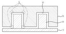
도 2a 내지 도 2c는 본 발명에 따른 백라이트 유닛의 구조를 설명하기 위한 개념도이다.
도 3은 본 발명에 따른 다른 실시예로서, 도 2a에 도시된 구조의 수용홈의 내측면에 일정한 경사를 가지도록 구현한 구조를 구비한 것이다.
도 4a 및 도 4b는 본 발명에 따른 또 다른 변형례를 도시한 것이다.
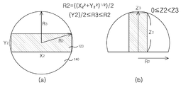
도 5a 및 도 5b는 본 발명에 따른 실시예의 다른 예를 도시한 것이다.
120: LED
121: 출사면
130: 도광판
140: 수용홈
A: 수용홈의 상부면
B: 수용홈의 내측면
E, E1, E2, E3: 에지부
Claims (7)
- 다수의 LED가 실장된 인쇄회로기판;
상기 LED를 수용하는 수용홈이 구비된 도광판;을 포함하여 구성되되,
상기 수용홈의 상부면 및 내측면이 만나 형성되는 에지부에 곡률을 구비한 곡률부가 적어도 1 이상 형성된 백라이트유닛.
- 청구항 1에 있어서,
상기 수용홈은,
도광판의 내부에 홀의 상부면과 개구된 구조의 하부면 및 내측면으로 구성되며,
상기 상부면과 하부면의 폭은 동일하거나, 또는 상기 하부면의 폭이 더 넓은 구조로 형성되는 백라이트 유닛.
- 청구항 2에 있어서,
상기 수용홈은 하부면이 개구된 직육면체 형상이며,
상기 곡률부는, 상기 수용홈의 상부면 단변의 길이의 1/2이하의 곡률반경(R)을 구비하는 백라이트 유닛.
- 청구항 1 내지 3 중 어느 한 항에 있어서,
상기 내측면과 상기 하부면이 만나 형성되는 에지부에 곡률을 형성한 제2곡률부를 적어도 1 이상 더 포함하는 백라이트 유닛.
- 청구항 4에 있어서,
상기 내측면 또는 상기 하부면의 연장선과 도광판의 하부평면의 연장선은 0≤θ≤90도의 범위에서 경사각을 이루는 백라이트 유닛.
- 청구항 1 내지 3 중 어느 한 항에 있어서,
상기 수용홈과 상기 LED의 이격거리(d)는 100mm이하의 범위에서 구현되는 백라이트 유닛.
- 청구항 1에 있어서,
상기 곡률부는,
상기 수용홈의 상부면 단변의 길이의 1/2 이상 상기 LED의 단면형상의 대각선의 길이의 1/2 이하의 곡률반경을 구비하는 백라이트 유닛.
Priority Applications (7)
| Application Number | Priority Date | Filing Date | Title |
|---|---|---|---|
| KR1020100113329A KR20120051945A (ko) | 2010-11-15 | 2010-11-15 | 백라이트유닛 |
| TW100140297A TWI615660B (zh) | 2010-11-15 | 2011-11-04 | 背光單元 |
| CN201180055048.7A CN103210343B (zh) | 2010-11-15 | 2011-11-10 | 背光单元 |
| EP11842386.2A EP2641128B1 (en) | 2010-11-15 | 2011-11-10 | Backlight unit |
| JP2013538644A JP5599517B2 (ja) | 2010-11-15 | 2011-11-10 | バックライトユニット |
| US13/885,631 US9207382B2 (en) | 2010-11-15 | 2011-11-10 | Light unit having light guide member with receiving holes with round part |
| PCT/KR2011/008534 WO2012067376A2 (en) | 2010-11-15 | 2011-11-10 | Backlight unit |
Applications Claiming Priority (1)
| Application Number | Priority Date | Filing Date | Title |
|---|---|---|---|
| KR1020100113329A KR20120051945A (ko) | 2010-11-15 | 2010-11-15 | 백라이트유닛 |
Publications (1)
| Publication Number | Publication Date |
|---|---|
| KR20120051945A true KR20120051945A (ko) | 2012-05-23 |
Family
ID=46084477
Family Applications (1)
| Application Number | Title | Priority Date | Filing Date |
|---|---|---|---|
| KR1020100113329A Ceased KR20120051945A (ko) | 2010-11-15 | 2010-11-15 | 백라이트유닛 |
Country Status (7)
| Country | Link |
|---|---|
| US (1) | US9207382B2 (ko) |
| EP (1) | EP2641128B1 (ko) |
| JP (1) | JP5599517B2 (ko) |
| KR (1) | KR20120051945A (ko) |
| CN (1) | CN103210343B (ko) |
| TW (1) | TWI615660B (ko) |
| WO (1) | WO2012067376A2 (ko) |
Cited By (2)
| Publication number | Priority date | Publication date | Assignee | Title |
|---|---|---|---|---|
| KR20190042717A (ko) * | 2016-12-09 | 2019-04-24 | 오므론 가부시키가이샤 | 도광판, 면 광원 장치, 표시 장치 및 전자 기기 |
| CN113820888A (zh) * | 2021-09-29 | 2021-12-21 | 联想(北京)有限公司 | 背光组件及其制作方法及显示装置 |
Families Citing this family (10)
| Publication number | Priority date | Publication date | Assignee | Title |
|---|---|---|---|---|
| US8858052B2 (en) * | 2010-03-31 | 2014-10-14 | Global Lighting Technology Inc. | Backlight module |
| EP2884160A1 (en) * | 2013-12-12 | 2015-06-17 | Defond Components Limited | Light panel |
| CN104776398A (zh) * | 2014-01-10 | 2015-07-15 | 广州奥翼电子科技有限公司 | 导光板、前光照明装置及电子纸显示屏 |
| CN104864369A (zh) * | 2014-02-21 | 2015-08-26 | 扬升照明股份有限公司 | 发光装置及光源模块 |
| CN104714270B (zh) * | 2015-03-20 | 2018-05-08 | 青岛海信移动通信技术股份有限公司 | 一种移动设备的导光膜及移动设备 |
| CN205027928U (zh) * | 2015-09-11 | 2016-02-10 | 京东方科技集团股份有限公司 | 导光板、背光源和智能手表 |
| US10203442B2 (en) * | 2015-10-30 | 2019-02-12 | Sharp Kabushiki Kaisha | Lighting device including a side emitting type light source for improved light efficiency and display device |
| US10147569B1 (en) * | 2017-09-11 | 2018-12-04 | Dell Products, L.P. | Keyboard backlight module |
| CN108388047A (zh) * | 2018-02-24 | 2018-08-10 | 惠科股份有限公司 | 一种背光模组及显示装置 |
| CN108897171B (zh) * | 2018-08-09 | 2021-03-12 | 京东方科技集团股份有限公司 | 背光模组和显示装置 |
Family Cites Families (15)
| Publication number | Priority date | Publication date | Assignee | Title |
|---|---|---|---|---|
| JP3427636B2 (ja) * | 1996-09-06 | 2003-07-22 | オムロン株式会社 | 面光源装置及び液晶表示装置 |
| JP3521301B2 (ja) * | 1997-03-14 | 2004-04-19 | オムロン株式会社 | 面光源装置 |
| JP2000267096A (ja) * | 1999-03-15 | 2000-09-29 | Matsushita Electric Ind Co Ltd | 液晶表示用バックライト装置 |
| US7557781B2 (en) * | 2003-01-06 | 2009-07-07 | Tpo Displays Corp. | Planar display structure with LED light source |
| JP2004212830A (ja) | 2003-01-08 | 2004-07-29 | Optrex Corp | 液晶表示素子用バックライト装置 |
| CN1297849C (zh) * | 2003-02-19 | 2007-01-31 | 明基电通股份有限公司 | 发光二极管背光模块 |
| JP4441854B2 (ja) * | 2003-11-25 | 2010-03-31 | オムロン株式会社 | 面光源装置及び当該装置を用いた機器 |
| JP4595595B2 (ja) * | 2005-03-08 | 2010-12-08 | ソニー株式会社 | バックライト装置及び液晶表示装置 |
| CN2896325Y (zh) * | 2006-03-21 | 2007-05-02 | 比乐达国际有限公司 | 显示器的发光二极管背光模组 |
| KR20070115129A (ko) * | 2006-05-30 | 2007-12-05 | 주식회사 엘티아이 | Led를 이용한 백라이트 유닛 |
| KR100989219B1 (ko) | 2006-06-30 | 2010-10-20 | 엘지디스플레이 주식회사 | 백라이트 어셈블리 및 이를 구비한 액정표시장치. |
| JP2008257900A (ja) | 2007-03-31 | 2008-10-23 | Nidec Copal Corp | 面発光装置 |
| JP2008305713A (ja) * | 2007-06-08 | 2008-12-18 | Fujifilm Corp | 面状照明装置 |
| JP5145957B2 (ja) | 2008-01-15 | 2013-02-20 | 凸版印刷株式会社 | 導光連結体、バックライトユニット、及び表示装置 |
| CN101749572B (zh) * | 2008-12-15 | 2012-10-10 | 鸿富锦精密工业(深圳)有限公司 | 发光模块 |
-
2010
- 2010-11-15 KR KR1020100113329A patent/KR20120051945A/ko not_active Ceased
-
2011
- 2011-11-04 TW TW100140297A patent/TWI615660B/zh active
- 2011-11-10 CN CN201180055048.7A patent/CN103210343B/zh active Active
- 2011-11-10 WO PCT/KR2011/008534 patent/WO2012067376A2/en not_active Ceased
- 2011-11-10 US US13/885,631 patent/US9207382B2/en active Active
- 2011-11-10 EP EP11842386.2A patent/EP2641128B1/en active Active
- 2011-11-10 JP JP2013538644A patent/JP5599517B2/ja not_active Expired - Fee Related
Cited By (4)
| Publication number | Priority date | Publication date | Assignee | Title |
|---|---|---|---|---|
| KR20190042717A (ko) * | 2016-12-09 | 2019-04-24 | 오므론 가부시키가이샤 | 도광판, 면 광원 장치, 표시 장치 및 전자 기기 |
| US10845524B2 (en) | 2016-12-09 | 2020-11-24 | Nichia Corporation | Light guide plate, planar light source apparatus, display apparatus, and electronic device |
| US11300722B2 (en) | 2016-12-09 | 2022-04-12 | Nichia Corporation | Light guide plate, planar light source apparatus, display apparatus, and electronic device |
| CN113820888A (zh) * | 2021-09-29 | 2021-12-21 | 联想(北京)有限公司 | 背光组件及其制作方法及显示装置 |
Also Published As
| Publication number | Publication date |
|---|---|
| US9207382B2 (en) | 2015-12-08 |
| WO2012067376A3 (en) | 2012-09-20 |
| JP2013544017A (ja) | 2013-12-09 |
| US20130250617A1 (en) | 2013-09-26 |
| WO2012067376A2 (en) | 2012-05-24 |
| EP2641128B1 (en) | 2018-04-25 |
| EP2641128A4 (en) | 2014-08-27 |
| EP2641128A2 (en) | 2013-09-25 |
| CN103210343B (zh) | 2017-03-08 |
| TW201224608A (en) | 2012-06-16 |
| CN103210343A (zh) | 2013-07-17 |
| TWI615660B (zh) | 2018-02-21 |
| JP5599517B2 (ja) | 2014-10-01 |
Similar Documents
| Publication | Publication Date | Title |
|---|---|---|
| KR20120051945A (ko) | 백라이트유닛 | |
| US8646932B2 (en) | Backlight unit and the display device having the same | |
| US7637646B2 (en) | Backlight assembly and liquid crystal display device having the same | |
| US8534853B2 (en) | Backlight module | |
| US8840297B2 (en) | Back-light module | |
| KR20110020010A (ko) | 측면 조광형 백라이트 장치의 도광판 | |
| US10852585B2 (en) | Light diffusing lens for light emitting device | |
| KR20110057528A (ko) | 백라이트 모듈 및 이를 포함한 액정표시장치 | |
| KR20080069010A (ko) | 백라이트 및 이를 포함하는 표시 장치 | |
| KR20120077414A (ko) | 백라이트 유닛 | |
| US9823507B2 (en) | Display device | |
| CN112230477A (zh) | 一种背光模组以及显示装置 | |
| CN213987113U (zh) | 一种背光模组以及显示装置 | |
| KR20120019784A (ko) | 직하형 백라이트 장치 | |
| US8743338B2 (en) | Liquid crystal display device | |
| KR20100086157A (ko) | 액정표시장치의 바텀 새시 | |
| KR100817838B1 (ko) | 측면형 백라이트 장치의 도광판 구조 | |
| KR101211716B1 (ko) | 백라이트 유닛 | |
| KR102533257B1 (ko) | 반사시트 및 이를 구비한 디스플레이 장치 | |
| KR20140077295A (ko) | 확산 발광 소자, 이를 이용한 엘이디 어레이 바 및 이를 갖는 백라이트 어셈블리 | |
| US9400348B2 (en) | Display backlight unit having reflecting structure for reducing hotspots | |
| KR101032532B1 (ko) | 측면 조광형 백라이트 장치 | |
| KR102443151B1 (ko) | 도광판 및 이를 구비하는 백라이트 장치 | |
| JP4671342B2 (ja) | バックライト | |
| JP6650884B2 (ja) | 面状光源 |
Legal Events
| Date | Code | Title | Description |
|---|---|---|---|
| A201 | Request for examination | ||
| PA0109 | Patent application |
Patent event code: PA01091R01D Comment text: Patent Application Patent event date: 20101115 |
|
| PA0201 | Request for examination | ||
| E902 | Notification of reason for refusal | ||
| PE0902 | Notice of grounds for rejection |
Comment text: Notification of reason for refusal Patent event date: 20120326 Patent event code: PE09021S01D |
|
| PG1501 | Laying open of application | ||
| AMND | Amendment | ||
| E601 | Decision to refuse application | ||
| PE0601 | Decision on rejection of patent |
Patent event date: 20121024 Comment text: Decision to Refuse Application Patent event code: PE06012S01D Patent event date: 20120326 Comment text: Notification of reason for refusal Patent event code: PE06011S01I |
|
| AMND | Amendment | ||
| PX0901 | Re-examination |
Patent event code: PX09011S01I Patent event date: 20121024 Comment text: Decision to Refuse Application Patent event code: PX09012R01I Patent event date: 20120529 Comment text: Amendment to Specification, etc. |
|
| PX0601 | Decision of rejection after re-examination |
Comment text: Decision to Refuse Application Patent event code: PX06014S01D Patent event date: 20121224 Comment text: Amendment to Specification, etc. Patent event code: PX06012R01I Patent event date: 20121123 Comment text: Decision to Refuse Application Patent event code: PX06011S01I Patent event date: 20121024 Comment text: Amendment to Specification, etc. Patent event code: PX06012R01I Patent event date: 20120529 Comment text: Notification of reason for refusal Patent event code: PX06013S01I Patent event date: 20120326 |
|
| J201 | Request for trial against refusal decision | ||
| PJ0201 | Trial against decision of rejection |
Patent event date: 20130125 Comment text: Request for Trial against Decision on Refusal Patent event code: PJ02012R01D Patent event date: 20121224 Comment text: Decision to Refuse Application Patent event code: PJ02011S01I Patent event date: 20121024 Comment text: Decision to Refuse Application Patent event code: PJ02011S01I Appeal kind category: Appeal against decision to decline refusal Appeal identifier: 2013101000576 Request date: 20130125 |
|
| J301 | Trial decision |
Free format text: TRIAL DECISION FOR APPEAL AGAINST DECISION TO DECLINE REFUSAL REQUESTED 20130125 Effective date: 20140421 |
|
| PJ1301 | Trial decision |
Patent event code: PJ13011S01D Patent event date: 20140421 Comment text: Trial Decision on Objection to Decision on Refusal Appeal kind category: Appeal against decision to decline refusal Request date: 20130125 Decision date: 20140421 Appeal identifier: 2013101000576 |