KR20120060480A - 수직 구조의 비휘발성 메모리 소자, 반도체 소자 및 시스템 - Google Patents
수직 구조의 비휘발성 메모리 소자, 반도체 소자 및 시스템 Download PDFInfo
- Publication number
- KR20120060480A KR20120060480A KR1020100122005A KR20100122005A KR20120060480A KR 20120060480 A KR20120060480 A KR 20120060480A KR 1020100122005 A KR1020100122005 A KR 1020100122005A KR 20100122005 A KR20100122005 A KR 20100122005A KR 20120060480 A KR20120060480 A KR 20120060480A
- Authority
- KR
- South Korea
- Prior art keywords
- layer
- impurity
- channel region
- memory cell
- substrate
- Prior art date
- Legal status (The legal status is an assumption and is not a legal conclusion. Google has not performed a legal analysis and makes no representation as to the accuracy of the status listed.)
- Ceased
Links
Images











Classifications
-
- H—ELECTRICITY
- H10—SEMICONDUCTOR DEVICES; ELECTRIC SOLID-STATE DEVICES NOT OTHERWISE PROVIDED FOR
- H10B—ELECTRONIC MEMORY DEVICES
- H10B43/00—EEPROM devices comprising charge-trapping gate insulators
- H10B43/20—EEPROM devices comprising charge-trapping gate insulators characterised by three-dimensional [3D] arrangements, e.g. with cells on different height levels
- H10B43/23—EEPROM devices comprising charge-trapping gate insulators characterised by three-dimensional [3D] arrangements, e.g. with cells on different height levels with source and drain on different levels, e.g. with sloping channels
- H10B43/27—EEPROM devices comprising charge-trapping gate insulators characterised by three-dimensional [3D] arrangements, e.g. with cells on different height levels with source and drain on different levels, e.g. with sloping channels the channels comprising vertical portions, e.g. U-shaped channels
-
- H—ELECTRICITY
- H10—SEMICONDUCTOR DEVICES; ELECTRIC SOLID-STATE DEVICES NOT OTHERWISE PROVIDED FOR
- H10D—INORGANIC ELECTRIC SEMICONDUCTOR DEVICES
- H10D30/00—Field-effect transistors [FET]
- H10D30/60—Insulated-gate field-effect transistors [IGFET]
- H10D30/69—IGFETs having charge trapping gate insulators, e.g. MNOS transistors
- H10D30/693—Vertical IGFETs having charge trapping gate insulators
-
- H—ELECTRICITY
- H10—SEMICONDUCTOR DEVICES; ELECTRIC SOLID-STATE DEVICES NOT OTHERWISE PROVIDED FOR
- H10D—INORGANIC ELECTRIC SEMICONDUCTOR DEVICES
- H10D84/00—Integrated devices formed in or on semiconductor substrates that comprise only semiconducting layers, e.g. on Si wafers or on GaAs-on-Si wafers
- H10D84/01—Manufacture or treatment
- H10D84/0123—Integrating together multiple components covered by H10D12/00 or H10D30/00, e.g. integrating multiple IGBTs
- H10D84/0126—Integrating together multiple components covered by H10D12/00 or H10D30/00, e.g. integrating multiple IGBTs the components including insulated gates, e.g. IGFETs
- H10D84/0149—Manufacturing their interconnections or electrodes, e.g. source or drain electrodes
-
- H—ELECTRICITY
- H10—SEMICONDUCTOR DEVICES; ELECTRIC SOLID-STATE DEVICES NOT OTHERWISE PROVIDED FOR
- H10D—INORGANIC ELECTRIC SEMICONDUCTOR DEVICES
- H10D84/00—Integrated devices formed in or on semiconductor substrates that comprise only semiconducting layers, e.g. on Si wafers or on GaAs-on-Si wafers
- H10D84/01—Manufacture or treatment
- H10D84/0123—Integrating together multiple components covered by H10D12/00 or H10D30/00, e.g. integrating multiple IGBTs
- H10D84/0126—Integrating together multiple components covered by H10D12/00 or H10D30/00, e.g. integrating multiple IGBTs the components including insulated gates, e.g. IGFETs
- H10D84/016—Integrating together multiple components covered by H10D12/00 or H10D30/00, e.g. integrating multiple IGBTs the components including insulated gates, e.g. IGFETs the components including vertical IGFETs
-
- H—ELECTRICITY
- H10—SEMICONDUCTOR DEVICES; ELECTRIC SOLID-STATE DEVICES NOT OTHERWISE PROVIDED FOR
- H10P—GENERIC PROCESSES OR APPARATUS FOR THE MANUFACTURE OR TREATMENT OF DEVICES COVERED BY CLASS H10
- H10P32/00—Diffusion of dopants within, into or out of wafers, substrates or parts of devices
- H10P32/10—Diffusion of dopants within, into or out of semiconductor bodies or layers
- H10P32/14—Diffusion of dopants within, into or out of semiconductor bodies or layers within a single semiconductor body or layer in a solid phase; between different semiconductor bodies or layers, both in a solid phase
- H10P32/1408—Diffusion of dopants within, into or out of semiconductor bodies or layers within a single semiconductor body or layer in a solid phase; between different semiconductor bodies or layers, both in a solid phase from or through or into an external applied layer, e.g. photoresist or nitride layers
- H10P32/141—Diffusion of dopants within, into or out of semiconductor bodies or layers within a single semiconductor body or layer in a solid phase; between different semiconductor bodies or layers, both in a solid phase from or through or into an external applied layer, e.g. photoresist or nitride layers the applied layer comprising oxides only
-
- H—ELECTRICITY
- H10—SEMICONDUCTOR DEVICES; ELECTRIC SOLID-STATE DEVICES NOT OTHERWISE PROVIDED FOR
- H10P—GENERIC PROCESSES OR APPARATUS FOR THE MANUFACTURE OR TREATMENT OF DEVICES COVERED BY CLASS H10
- H10P32/00—Diffusion of dopants within, into or out of wafers, substrates or parts of devices
- H10P32/10—Diffusion of dopants within, into or out of semiconductor bodies or layers
- H10P32/17—Diffusion of dopants within, into or out of semiconductor bodies or layers characterised by the semiconductor material
- H10P32/171—Diffusion of dopants within, into or out of semiconductor bodies or layers characterised by the semiconductor material being group IV material
Landscapes
- Semiconductor Memories (AREA)
- Non-Volatile Memory (AREA)
Abstract
Description
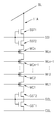
도 2는 본 발명의 다른 실시예에 따른 비휘발성 메모리 소자의 메모리 셀 스트링의 등가회로도이다.
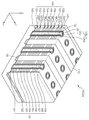
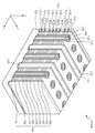
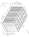
도 3은 본 발명의 제1 실시예에 따른 비휘발성 메모리 소자의 메모리 셀 스트링들의 3차원 구조를 나타내는 개략적인 사시도이다.
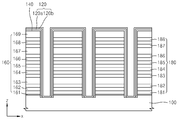
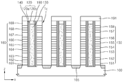
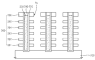
도 4a 내지 도 4h는 도 3의 비휘발성 메모리 소자의 제조 방법을 설명하기 위한 단면도들이다.
도 5는 본 발명의 제2 실시예에 따른 비휘발성 메모리 소자의 메모리 셀 스트링들의 3차원 구조를 나타내는 개략적인 사시도이다.
도 6은 본 발명의 제3 실시예에 따른 비휘발성 메모리 소자의 메모리 셀 스트링들의 3차원 구조를 나타내는 개략적인 사시도이다.
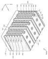
도 7은 본 발명의 제4 실시예에 따른 비휘발성 메모리 소자의 메모리 셀 스트링들의 3차원 구조를 나타내는 개략적인 사시도이다.
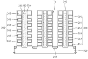
도 8a 내지 도 8f는 도 7의 비휘발성 메모리 소자의 제조 방법을 설명하기 위한 단면도들이다.
도 9는 본 발명의 제5 실시예에 따른 비휘발성 메모리 소자의 메모리 셀 스트링들의 3차원 구조를 나타내는 개략적인 사시도이다.
도 10은 본 발명의 제6 실시예에 따른 비휘발성 메모리 소자의 메모리 셀 스트링들의 3차원 구조를 나타내는 개략적인 사시도이다.
도 11a 및 도 11b는 본 발명의 일 실시예에 따른 비휘발성 메모리 소자의 HTS(hot temperature stress) 특성을 보여주는 시뮬레이션 결과들이다.
도 12는 본 발명의 다른 실시예에 따른 비휘발성 메모리 소자의 개략적인 블록 다이어그램이다.
도 13은 본 발명의 일 실시예에 따른 메모리 카드를 보여주는 개략도이다.
도 14는 본 발명의 일 실시예에 따른 전자 시스템을 보여주는 블록도이다.
110, 210: 공통 소스 라인 120, 220: 채널 영역
125, 225: 확산 제어층 130, 230: 불순물 제공층
140, 240: 게이트 유전막 142, 242: 터널링 절연층
144, 244: 전하 저장층 146, 246: 블록킹 절연층
150, 250: 게이트 전극 160, 260: 층간 절연층
170, 270: 절연 영역 175, 275: 절연층
180, 280: 희생층 190, 290: 도전층
Claims (10)
- 기판 상으로 수직 신장하고, 불순물을 포함하는 채널 영역;
상기 채널 영역의 외측벽을 따라서 상기 기판 상으로 수직 신장하고, 복수의 메모리 셀들 및 상기 복수의 메모리 셀들의 일측에 배치된 적어도 하나의 선택 트랜지스터를 포함하며 서로 인접하는 복수의 메모리 셀 스트링들; 및
상기 채널 영역의 내측에 위치하고, 불순물을 포함하는 불순물 제공층;
을 포함하는 수직 구조의 비휘발성 메모리 소자. - 제1 항에 있어서,
상기 불순물 제공층은 불순물이 도핑된 절연성 물질 또는 불순물이 도핑된 반도체 물질을 포함하는 것을 특징으로 하는 수직 구조의 비휘발성 메모리 소자. - 제1 항에 있어서,
상기 채널 영역은 제1 불순물 농도를 가지며, 상기 불순물 제공층은 상기 제1 불순물 농도보다 높은 제2 불순물 농도를 가지는 것을 특징으로 하는 수직 구조의 비휘발성 메모리 소자. - 제1 항에 있어서,
상기 채널 영역은 상기 기판과 전기적으로 연결되는 것을 특징으로 하는 수직 구조의 비휘발성 메모리 소자. - 제1 항에 있어서,
상기 채널 영역 및 상기 불순물 제공층의 사이에 위치한 확산 제어층을 더 포함하는 것을 특징으로 하는 수직 구조의 비휘발성 메모리 소자. - 제5 항에 있어서,
상기 확산 제어층은 상기 불순물 제공층으로부터 상기 채널 영역으로 확산되는 불순물의 확산 속도를 감소시키는 것을 특징으로 하는 수직 구조의 비휘발성 메모리 소자. - 제1 항에 있어서,
상기 불순물 제공층은 PSG(PhosphoSilicate Glass), BSG(BoroSilicate Glass) 또는 도핑된 폴리 실리콘 중 어느 하나를 포함하는 것을 특징으로 하는 수직 구조의 비휘발성 메모리 소자. - 제1 항에 있어서,
상기 메모리 셀 스트링의 일단에 연결된 비트 라인; 및
상기 비트 라인 반대편에서 상기 메모리 셀 스트링의 타단에 연결된 공통 소스 라인을 더 포함하는 것을 특징으로 하는 수직 구조의 비휘발성 메모리 소자. - 제1 항에 있어서,
상기 복수의 메모리 셀들 및 상기 적어도 하나의 선택 트랜지스터는 상기 복수의 채널 영역들의 측벽 상의 게이트 유전막 및 게이트 전극을 포함하는 것을 특징으로 하는 수직 구조의 비휘발성 메모리 소자. - 제9 항에 있어서,
상기 게이트 유전막은, 상기 채널 영역으로부터 순차적으로 적층된 터널링 절연층, 전하 저장층 및 블록킹 절연층을 포함하는 것을 특징으로 하는 수직 구조의 비휘발성 메모리 소자.
Priority Applications (2)
| Application Number | Priority Date | Filing Date | Title |
|---|---|---|---|
| KR1020100122005A KR20120060480A (ko) | 2010-12-02 | 2010-12-02 | 수직 구조의 비휘발성 메모리 소자, 반도체 소자 및 시스템 |
| US13/238,368 US20120139027A1 (en) | 2010-12-02 | 2011-09-21 | Vertical structure non-volatile memory devices including impurity providing layer |
Applications Claiming Priority (1)
| Application Number | Priority Date | Filing Date | Title |
|---|---|---|---|
| KR1020100122005A KR20120060480A (ko) | 2010-12-02 | 2010-12-02 | 수직 구조의 비휘발성 메모리 소자, 반도체 소자 및 시스템 |
Publications (1)
| Publication Number | Publication Date |
|---|---|
| KR20120060480A true KR20120060480A (ko) | 2012-06-12 |
Family
ID=46161416
Family Applications (1)
| Application Number | Title | Priority Date | Filing Date |
|---|---|---|---|
| KR1020100122005A Ceased KR20120060480A (ko) | 2010-12-02 | 2010-12-02 | 수직 구조의 비휘발성 메모리 소자, 반도체 소자 및 시스템 |
Country Status (2)
| Country | Link |
|---|---|
| US (1) | US20120139027A1 (ko) |
| KR (1) | KR20120060480A (ko) |
Cited By (4)
| Publication number | Priority date | Publication date | Assignee | Title |
|---|---|---|---|---|
| KR20150028885A (ko) * | 2013-08-30 | 2015-03-17 | 삼성전자주식회사 | 수직 채널 영역을 구비하는 3차원 구조의 비휘발성 메모리 소자 |
| KR20160029981A (ko) * | 2014-09-05 | 2016-03-16 | 삼성전자주식회사 | 반도체 장치 |
| US9876026B2 (en) | 2015-07-10 | 2018-01-23 | SK Hynix Inc. | Method of manufacturing semiconductor device |
| KR20200076806A (ko) * | 2018-12-19 | 2020-06-30 | 삼성전자주식회사 | 수직형 메모리 장치 |
Families Citing this family (24)
| Publication number | Priority date | Publication date | Assignee | Title |
|---|---|---|---|---|
| KR101735810B1 (ko) * | 2010-08-20 | 2017-05-16 | 삼성전자주식회사 | 3차원 반도체 장치 |
| KR101855437B1 (ko) * | 2010-12-02 | 2018-05-08 | 삼성전자주식회사 | 불휘발성 메모리 장치 및 그것의 동작 방법 |
| KR20120069034A (ko) * | 2010-12-20 | 2012-06-28 | 삼성전자주식회사 | 수직형 메모리 장치 및 그 제조 방법 |
| KR101916222B1 (ko) * | 2011-04-29 | 2018-11-08 | 삼성전자 주식회사 | 수직 구조의 비휘발성 메모리 소자 및 그 제조 방법 |
| KR20130072911A (ko) * | 2011-12-22 | 2013-07-02 | 에스케이하이닉스 주식회사 | 비휘발성 메모리 장치 및 그 제조 방법 |
| KR20130076461A (ko) * | 2011-12-28 | 2013-07-08 | 에스케이하이닉스 주식회사 | 비휘발성 메모리 장치 및 그 제조 방법 |
| KR20130130480A (ko) * | 2012-05-22 | 2013-12-02 | 삼성전자주식회사 | 3차원 반도체 메모리 장치 및 그 형성 방법 |
| KR20140029707A (ko) * | 2012-08-29 | 2014-03-11 | 에스케이하이닉스 주식회사 | 수직 채널들을 갖는 반도체 메모리 소자와 이를 포함하는 메모리 시스템과 이의 제조방법 |
| KR102074982B1 (ko) * | 2013-04-09 | 2020-02-10 | 에스케이하이닉스 주식회사 | 비휘발성 메모리 장치 및 그 제조 방법 |
| US9018064B2 (en) * | 2013-07-10 | 2015-04-28 | Varian Semiconductor Equipment Associates, Inc. | Method of doping a polycrystalline transistor channel for vertical NAND devices |
| KR102094472B1 (ko) * | 2013-10-08 | 2020-03-27 | 삼성전자주식회사 | 반도체 장치 |
| KR20150061395A (ko) * | 2013-11-27 | 2015-06-04 | 삼성전자주식회사 | 반도체 장치 및 그 제조 방법 |
| KR20150064520A (ko) * | 2013-12-03 | 2015-06-11 | 에스케이하이닉스 주식회사 | 반도체 장치 및 그 제조방법 |
| KR20150085735A (ko) * | 2014-01-16 | 2015-07-24 | 삼성전자주식회사 | 반도체 소자 및 그 제조방법 |
| KR20160013765A (ko) * | 2014-07-28 | 2016-02-05 | 삼성전자주식회사 | 반도체 장치 |
| US9711524B2 (en) * | 2015-01-13 | 2017-07-18 | Sandisk Technologies Llc | Three-dimensional memory device containing plural select gate transistors having different characteristics and method of making thereof |
| US9659958B2 (en) | 2015-10-13 | 2017-05-23 | Samsung Elctronics Co., Ltd. | Three-dimensional semiconductor memory device |
| US9853049B2 (en) * | 2016-04-21 | 2017-12-26 | Samsung Electronics Co., Ltd. | Memory devices having common source lines including layers of different materials |
| KR102331474B1 (ko) * | 2017-06-19 | 2021-11-29 | 삼성전자주식회사 | 반도체 장치 |
| KR20200051301A (ko) | 2018-11-05 | 2020-05-13 | 에스케이하이닉스 주식회사 | 3차원 비휘발성 메모리 장치 및 그 제조방법 |
| KR102662190B1 (ko) * | 2018-12-17 | 2024-05-02 | 에스케이하이닉스 주식회사 | 3차원 비휘발성 메모리 장치의 제조방법 |
| CN112151553B (zh) * | 2020-07-21 | 2024-06-11 | 长江存储科技有限责任公司 | 3d存储器件的制造方法 |
| JP7502122B2 (ja) * | 2020-09-09 | 2024-06-18 | キオクシア株式会社 | 半導体装置およびその製造方法 |
| CN113540112B (zh) * | 2021-07-20 | 2022-11-18 | 长江存储科技有限责任公司 | 三维存储器及其制造方法 |
Family Cites Families (11)
| Publication number | Priority date | Publication date | Assignee | Title |
|---|---|---|---|---|
| US5756385A (en) * | 1994-03-30 | 1998-05-26 | Sandisk Corporation | Dense flash EEPROM cell array and peripheral supporting circuits formed in deposited field oxide with the use of spacers |
| JP4822841B2 (ja) * | 2005-12-28 | 2011-11-24 | 株式会社東芝 | 半導体記憶装置及びその製造方法 |
| JP4772656B2 (ja) * | 2006-12-21 | 2011-09-14 | 株式会社東芝 | 不揮発性半導体メモリ |
| US7906818B2 (en) * | 2008-03-13 | 2011-03-15 | Micron Technology, Inc. | Memory array with a pair of memory-cell strings to a single conductive pillar |
| KR101527192B1 (ko) * | 2008-12-10 | 2015-06-10 | 삼성전자주식회사 | 불휘발성 메모리 소자 및 그의 제조방법 |
| KR101551901B1 (ko) * | 2008-12-31 | 2015-09-09 | 삼성전자주식회사 | 반도체 기억 소자 및 그 형성 방법 |
| KR101512494B1 (ko) * | 2009-01-09 | 2015-04-16 | 삼성전자주식회사 | 반도체 장치의 제조 방법 |
| KR101532366B1 (ko) * | 2009-02-25 | 2015-07-01 | 삼성전자주식회사 | 반도체 기억 소자 |
| KR101102506B1 (ko) * | 2009-06-12 | 2012-01-04 | 주식회사 하이닉스반도체 | 수직채널형 비휘발성 메모리 소자 제조 방법 |
| KR101096199B1 (ko) * | 2009-09-07 | 2011-12-22 | 주식회사 하이닉스반도체 | 수직채널형 비휘발성 메모리 소자 제조 방법 |
| JP2011170956A (ja) * | 2010-02-18 | 2011-09-01 | Samsung Electronics Co Ltd | 不揮発性メモリ装置およびそのプログラム方法と、それを含むメモリシステム |
-
2010
- 2010-12-02 KR KR1020100122005A patent/KR20120060480A/ko not_active Ceased
-
2011
- 2011-09-21 US US13/238,368 patent/US20120139027A1/en not_active Abandoned
Cited By (4)
| Publication number | Priority date | Publication date | Assignee | Title |
|---|---|---|---|---|
| KR20150028885A (ko) * | 2013-08-30 | 2015-03-17 | 삼성전자주식회사 | 수직 채널 영역을 구비하는 3차원 구조의 비휘발성 메모리 소자 |
| KR20160029981A (ko) * | 2014-09-05 | 2016-03-16 | 삼성전자주식회사 | 반도체 장치 |
| US9876026B2 (en) | 2015-07-10 | 2018-01-23 | SK Hynix Inc. | Method of manufacturing semiconductor device |
| KR20200076806A (ko) * | 2018-12-19 | 2020-06-30 | 삼성전자주식회사 | 수직형 메모리 장치 |
Also Published As
| Publication number | Publication date |
|---|---|
| US20120139027A1 (en) | 2012-06-07 |
Similar Documents
| Publication | Publication Date | Title |
|---|---|---|
| KR101845511B1 (ko) | 수직 구조의 비휘발성 메모리 소자 제조 방법 | |
| KR20120060480A (ko) | 수직 구조의 비휘발성 메모리 소자, 반도체 소자 및 시스템 | |
| KR101736982B1 (ko) | 수직 구조의 비휘발성 메모리 소자 | |
| USRE49440E1 (en) | Vertical-type non-volatile memory devices having dummy channel holes | |
| KR101809512B1 (ko) | 비휘발성 메모리 소자 및 그 제조 방법 | |
| KR101549858B1 (ko) | 수직 채널 구조의 플래쉬 메모리 소자 | |
| JP5288877B2 (ja) | 不揮発性半導体記憶装置 | |
| KR101916222B1 (ko) | 수직 구조의 비휘발성 메모리 소자 및 그 제조 방법 | |
| CN106601752B (zh) | 三维半导体存储装置和竖直集成电路装置 | |
| KR102101841B1 (ko) | 수직형 비휘발성 메모리 소자 | |
| US8877591B2 (en) | Methods of manufacturing vertical structure nonvolatile memory devices | |
| KR101660432B1 (ko) | 수직 구조의 반도체 메모리 소자 | |
| KR20120068392A (ko) | 비휘발성 메모리 소자 및 반도체 소자의 콘택 플러그의 제조 방법 | |
| KR101916223B1 (ko) | 반도체 장치 및 그 제조 방법 | |
| KR101845507B1 (ko) | 수직 구조의 비휘발성 메모리 소자 및 그 제조 방법 | |
| KR101834930B1 (ko) | 수직 구조의 비휘발성 메모리 소자 | |
| CN110581135A (zh) | 半导体器件及其制造方法 | |
| KR20110003764A (ko) | 메탈 소스 라인을 갖는 수직 구조의 비휘발성 메모리 소자의 제조방법 | |
| JP2009164485A (ja) | 不揮発性半導体記憶装置 | |
| KR20100091835A (ko) | 수직 폴딩 구조의 비휘발성 메모리 소자 및 그 제조 방법 | |
| KR20120128438A (ko) | 수직 구조의 비휘발성 메모리 소자, 반도체 소자 및 시스템 | |
| KR20130038032A (ko) | 수직 구조의 비휘발성 메모리 소자 |
Legal Events
| Date | Code | Title | Description |
|---|---|---|---|
| PA0109 | Patent application |
Patent event code: PA01091R01D Comment text: Patent Application Patent event date: 20101202 |
|
| PG1501 | Laying open of application | ||
| A201 | Request for examination | ||
| PA0201 | Request for examination |
Patent event code: PA02012R01D Patent event date: 20151106 Comment text: Request for Examination of Application Patent event code: PA02011R01I Patent event date: 20101202 Comment text: Patent Application |
|
| E902 | Notification of reason for refusal | ||
| PE0902 | Notice of grounds for rejection |
Comment text: Notification of reason for refusal Patent event date: 20170329 Patent event code: PE09021S01D |
|
| E601 | Decision to refuse application | ||
| PE0601 | Decision on rejection of patent |
Patent event date: 20170607 Comment text: Decision to Refuse Application Patent event code: PE06012S01D Patent event date: 20170329 Comment text: Notification of reason for refusal Patent event code: PE06011S01I |