KR20120080366A - 발광 모듈, 이의 제조 방법 및 이를 포함하는 표시 장치 - Google Patents
발광 모듈, 이의 제조 방법 및 이를 포함하는 표시 장치 Download PDFInfo
- Publication number
- KR20120080366A KR20120080366A KR1020110001778A KR20110001778A KR20120080366A KR 20120080366 A KR20120080366 A KR 20120080366A KR 1020110001778 A KR1020110001778 A KR 1020110001778A KR 20110001778 A KR20110001778 A KR 20110001778A KR 20120080366 A KR20120080366 A KR 20120080366A
- Authority
- KR
- South Korea
- Prior art keywords
- lead
- light emitting
- light
- guide plate
- emitting chip
- Prior art date
- Legal status (The legal status is an assumption and is not a legal conclusion. Google has not performed a legal analysis and makes no representation as to the accuracy of the status listed.)
- Ceased
Links
Images




Classifications
-
- H—ELECTRICITY
- H10—SEMICONDUCTOR DEVICES; ELECTRIC SOLID-STATE DEVICES NOT OTHERWISE PROVIDED FOR
- H10H—INORGANIC LIGHT-EMITTING SEMICONDUCTOR DEVICES HAVING POTENTIAL BARRIERS
- H10H20/00—Individual inorganic light-emitting semiconductor devices having potential barriers, e.g. light-emitting diodes [LED]
- H10H20/80—Constructional details
- H10H20/85—Packages
- H10H20/858—Means for heat extraction or cooling
- H10H20/8582—Means for heat extraction or cooling characterised by their shape
-
- G—PHYSICS
- G02—OPTICS
- G02B—OPTICAL ELEMENTS, SYSTEMS OR APPARATUS
- G02B6/00—Light guides; Structural details of arrangements comprising light guides and other optical elements, e.g. couplings
- G02B6/0001—Light guides; Structural details of arrangements comprising light guides and other optical elements, e.g. couplings specially adapted for lighting devices or systems
- G02B6/0011—Light guides; Structural details of arrangements comprising light guides and other optical elements, e.g. couplings specially adapted for lighting devices or systems the light guides being planar or of plate-like form
- G02B6/0081—Mechanical or electrical aspects of the light guide and light source in the lighting device peculiar to the adaptation to planar light guides, e.g. concerning packaging
- G02B6/0083—Details of electrical connections of light sources to drivers, circuit boards, or the like
-
- G—PHYSICS
- G02—OPTICS
- G02B—OPTICAL ELEMENTS, SYSTEMS OR APPARATUS
- G02B6/00—Light guides; Structural details of arrangements comprising light guides and other optical elements, e.g. couplings
- G02B6/0001—Light guides; Structural details of arrangements comprising light guides and other optical elements, e.g. couplings specially adapted for lighting devices or systems
- G02B6/0011—Light guides; Structural details of arrangements comprising light guides and other optical elements, e.g. couplings specially adapted for lighting devices or systems the light guides being planar or of plate-like form
- G02B6/0081—Mechanical or electrical aspects of the light guide and light source in the lighting device peculiar to the adaptation to planar light guides, e.g. concerning packaging
- G02B6/0086—Positioning aspects
- G02B6/0088—Positioning aspects of the light guide or other optical sheets in the package
-
- G—PHYSICS
- G02—OPTICS
- G02B—OPTICAL ELEMENTS, SYSTEMS OR APPARATUS
- G02B6/00—Light guides; Structural details of arrangements comprising light guides and other optical elements, e.g. couplings
- G02B6/0001—Light guides; Structural details of arrangements comprising light guides and other optical elements, e.g. couplings specially adapted for lighting devices or systems
- G02B6/0011—Light guides; Structural details of arrangements comprising light guides and other optical elements, e.g. couplings specially adapted for lighting devices or systems the light guides being planar or of plate-like form
- G02B6/0081—Mechanical or electrical aspects of the light guide and light source in the lighting device peculiar to the adaptation to planar light guides, e.g. concerning packaging
- G02B6/0086—Positioning aspects
- G02B6/009—Positioning aspects of the light source in the package
-
- G—PHYSICS
- G02—OPTICS
- G02B—OPTICAL ELEMENTS, SYSTEMS OR APPARATUS
- G02B6/00—Light guides; Structural details of arrangements comprising light guides and other optical elements, e.g. couplings
- G02B6/0001—Light guides; Structural details of arrangements comprising light guides and other optical elements, e.g. couplings specially adapted for lighting devices or systems
- G02B6/0011—Light guides; Structural details of arrangements comprising light guides and other optical elements, e.g. couplings specially adapted for lighting devices or systems the light guides being planar or of plate-like form
- G02B6/0081—Mechanical or electrical aspects of the light guide and light source in the lighting device peculiar to the adaptation to planar light guides, e.g. concerning packaging
- G02B6/0086—Positioning aspects
- G02B6/0091—Positioning aspects of the light source relative to the light guide
-
- H—ELECTRICITY
- H10—SEMICONDUCTOR DEVICES; ELECTRIC SOLID-STATE DEVICES NOT OTHERWISE PROVIDED FOR
- H10H—INORGANIC LIGHT-EMITTING SEMICONDUCTOR DEVICES HAVING POTENTIAL BARRIERS
- H10H20/00—Individual inorganic light-emitting semiconductor devices having potential barriers, e.g. light-emitting diodes [LED]
- H10H20/01—Manufacture or treatment
- H10H20/036—Manufacture or treatment of packages
- H10H20/0364—Manufacture or treatment of packages of interconnections
-
- H—ELECTRICITY
- H10—SEMICONDUCTOR DEVICES; ELECTRIC SOLID-STATE DEVICES NOT OTHERWISE PROVIDED FOR
- H10H—INORGANIC LIGHT-EMITTING SEMICONDUCTOR DEVICES HAVING POTENTIAL BARRIERS
- H10H20/00—Individual inorganic light-emitting semiconductor devices having potential barriers, e.g. light-emitting diodes [LED]
- H10H20/80—Constructional details
- H10H20/85—Packages
- H10H20/852—Encapsulations
- H10H20/853—Encapsulations characterised by their shape
-
- H—ELECTRICITY
- H10—SEMICONDUCTOR DEVICES; ELECTRIC SOLID-STATE DEVICES NOT OTHERWISE PROVIDED FOR
- H10H—INORGANIC LIGHT-EMITTING SEMICONDUCTOR DEVICES HAVING POTENTIAL BARRIERS
- H10H20/00—Individual inorganic light-emitting semiconductor devices having potential barriers, e.g. light-emitting diodes [LED]
- H10H20/80—Constructional details
- H10H20/85—Packages
- H10H20/857—Interconnections, e.g. lead-frames, bond wires or solder balls
-
- G—PHYSICS
- G02—OPTICS
- G02F—OPTICAL DEVICES OR ARRANGEMENTS FOR THE CONTROL OF LIGHT BY MODIFICATION OF THE OPTICAL PROPERTIES OF THE MEDIA OF THE ELEMENTS INVOLVED THEREIN; NON-LINEAR OPTICS; FREQUENCY-CHANGING OF LIGHT; OPTICAL LOGIC ELEMENTS; OPTICAL ANALOGUE/DIGITAL CONVERTERS
- G02F1/00—Devices or arrangements for the control of the intensity, colour, phase, polarisation or direction of light arriving from an independent light source, e.g. switching, gating or modulating; Non-linear optics
- G02F1/01—Devices or arrangements for the control of the intensity, colour, phase, polarisation or direction of light arriving from an independent light source, e.g. switching, gating or modulating; Non-linear optics for the control of the intensity, phase, polarisation or colour
- G02F1/13—Devices or arrangements for the control of the intensity, colour, phase, polarisation or direction of light arriving from an independent light source, e.g. switching, gating or modulating; Non-linear optics for the control of the intensity, phase, polarisation or colour based on liquid crystals, e.g. single liquid crystal display cells
- G02F1/133—Constructional arrangements; Operation of liquid crystal cells; Circuit arrangements
- G02F1/1333—Constructional arrangements; Manufacturing methods
- G02F1/1335—Structural association of cells with optical devices, e.g. polarisers or reflectors
- G02F1/1336—Illuminating devices
- G02F1/133615—Edge-illuminating devices, i.e. illuminating from the side
-
- H—ELECTRICITY
- H10—SEMICONDUCTOR DEVICES; ELECTRIC SOLID-STATE DEVICES NOT OTHERWISE PROVIDED FOR
- H10W—GENERIC PACKAGES, INTERCONNECTIONS, CONNECTORS OR OTHER CONSTRUCTIONAL DETAILS OF DEVICES COVERED BY CLASS H10
- H10W72/00—Interconnections or connectors in packages
- H10W72/01—Manufacture or treatment
- H10W72/0198—Manufacture or treatment batch processes
-
- H—ELECTRICITY
- H10—SEMICONDUCTOR DEVICES; ELECTRIC SOLID-STATE DEVICES NOT OTHERWISE PROVIDED FOR
- H10W—GENERIC PACKAGES, INTERCONNECTIONS, CONNECTORS OR OTHER CONSTRUCTIONAL DETAILS OF DEVICES COVERED BY CLASS H10
- H10W90/00—Package configurations
- H10W90/701—Package configurations characterised by the relative positions of pads or connectors relative to package parts
- H10W90/751—Package configurations characterised by the relative positions of pads or connectors relative to package parts of bond wires
- H10W90/756—Package configurations characterised by the relative positions of pads or connectors relative to package parts of bond wires between a chip and a stacked lead frame, conducting package substrate or heat sink
Landscapes
- Physics & Mathematics (AREA)
- General Physics & Mathematics (AREA)
- Optics & Photonics (AREA)
- Planar Illumination Modules (AREA)
- Led Device Packages (AREA)
- Liquid Crystal (AREA)
Abstract
Description
도 2는 도 1의 I-I'선을 따라 절단한 단면도이다.
도 3은 도 1에 도시된 발광 모듈의 일부를 나타내는 투영 사시도이다.
도 4는 도 3의 II-II'선을 따라 절단한 단면도이다.
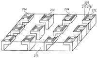
도 5a 내지 5g는 도 1에 도시된 발광 모듈의 제조 방법을 나타내는 사시도들이다.
도 6은 본 발명의 다른 실시예에 따른 발광 모듈을 나타내는 단면도이다.
도 7은 본 발명의 또 다른 실시예에 따른 표시 장치의 분해 사시도이다.
도 8은 도 7의 III-III'선을 따라 절단한 단면도이다.
도 9는 본 발명의 또 다른 실시예에 따른 표시 장치의 분해 사시도이다.
도 10은 도 9에 도시된 발광 모듈의 단면도이다.
도 11은 도 9의 'A' 부분을 나타내는 확대 평면도이다.
120: 액정 표시 패널 130, 140: 몰드 프레임
320: 광학 시트들 200, 210, 230: 발광 모듈
240, 260: 발광 패키지 230, 270, 290: 리드 프레임
310, 340, 360: 도광판 330: 반사판
350: 수납 용기
Claims (20)
- 광을 발생하는 발광칩, 상기 발광칩과 전기적으로 연결되는 제1 리드, 및 상기 제1 리드와 이격되고 상기 발광칩과 전기적으로 연결되는 제2 리드를 포함하는 발광 패키지; 및
상기 발광 패키지를 실장하며, 상기 제1 리드에 전기적으로 연결되는 제3 리드, 상기 제2 리드에 전기적으로 연결되는 제4 리드, 및 상기 제3 리드 및 상기 제4 리드를 몰딩하는 몰딩부를 포함하는 리드 프레임을 포함하는 발광 모듈. - 제1항에 있어서, 상기 제3 리드 및 상기 제4 리드는 사각 형상 및 라인형상의 회로 패턴을 포함하는 것을 특징으로 하는 발광 모듈.
- 제1항에 있어서,
상기 광은 상기 리드 프레임이 배치된 방향과 반대방향으로 출사되는 것을 특징으로 하는 발광 모듈. - 제1항에 있어서,
상기 발광칩을 수납하고, 상기 발광칩으로부터 발생하는 광을 출사하기 위한 개구가 형성된 케이스를 더 포함하고,
상기 케이스의 폭은 상기 리드 프레임의 폭과 동일한 것을 특징으로 하는 발광 모듈. - 제1항에 있어서, 상기 몰딩부는 바(bar) 형상으로 형성되어, 상기 발광칩을 복수 개 실장하는 것을 특징으로 하는 발광 모듈.
- 제1항에 있어서, 상기 발광 패키지는 상기 발광칩을 실장하는 제5 리드를 더 포함하고, 상기 리드 프레임은 상기 제5 리드와 연결되어 상기 발광칩으로부터 발생하는 열을 외부로 전달하는 열전달부를 더 포함하는 것을 특징으로 하는 발광 모듈.
- 광을 발생하는 발광칩, 상기 발광칩과 전기적으로 연결되는 제1 리드, 및 상기 발광칩과 전기적으로 연결되는 제2 리드를 각각 포함하는 발광 패키지들을 형성하는 단계;
상기 제1 리드에 전기적으로 연결되는 제3 리드 및 상기 제2 리드에 전기적으로 연결되는 제4 리드를 형성하는 단계;
상기 제3 리드 및 상기 제4 리드를 몰딩 수지로 커버하는 단계;
상기 몰딩 수지를 경화시켜 리드 프레임을 형성하는 단계;
상기 발광 패키지들을 행렬 형태로 상기 리드 프레임 상에 실장하는 단계; 및
상기 발광 패키지들이 실장된 상기 리드 프레임을 행 방향으로 절단하는 단계를 포함하는 발광 모듈의 제조 방법. - 제7항에 있어서, 상기 발광 패키지들을 행렬 형태로 상기 리드 프레임 상에 실장하는 단계는 표면 실장 기술(SMT: Surface Mount Technology)을 이용하는 것을 특징으로 하는 발광 모듈의 제조 방법.
- 제7항에 있어서, 상기 제3 리드 및 상기 제4 리드를 형성하는 단계는,
상기 제3 리드 및 상기 제4 리드에 펀칭(punching) 또는 포토 마스트(photo mask) 공법을 이용하여 회로 패턴을 형성하는 단계를 포함하는 것을 특징으로 하는 발광 모듈의 제조 방법. - 광이 입사되는 입사면 및 상기 입사면과 연결되고 상기 입사면을 통해 제공 받은 광을 출사하는 출사면을 포함하는 도광판;
상기 입사면에 제공되는 광을 발생하는 발광칩, 상기 발광칩과 전기적으로 연결되는 제1 리드 및 상기 제1 리드와 이격되고 상기 발광칩과 전기적으로 연결되는 제2 리드를 포함하는 발광 패키지, 및 상기 발광 패키지를 실장하며, 상기 제1 리드에 전기적으로 연결되는 제3 리드, 상기 제2 리드에 전기적으로 연결되는 제4 리드 및 상기 제3 리드 및 상기 제4 리드를 몰딩하는 몰딩부를 포함하는 리드 프레임을 포함하는 발광 모듈; 및
상기 도광판의 출사면으로부터 출사되는 광을 이용하여 영상을 표시하는 표시 패널을 포함하는 표시 장치. - 제8항에 있어서, 바닥부 및 상기 바닥부로부터 연장된 측벽부를 포함하여, 상기 도광판 및 상기 발광 모듈을 수납하는 수납 용기를 더 포함하며,
상기 수납 용기의 측벽부는 상기 도광판의 입사면과 마주하며, 상기 리드 프레임은 상기 측벽부 상에 배치되는 것을 특징으로 하는 표시 장치. - 제10항에 있어서, 상기 발광 패키지는 상기 발광칩을 실장하는 제5 리드를 더 포함하고, 상기 리드 프레임은 상기 제5 리드와 연결되어 상기 발광칩으로부터 발생하는 열을 외부로 전달하는 열전달부를 더 포함하는 것을 특징으로 하는 발광 모듈.
- 제12항에 있어서, 상기 열전달부는 상기 수납 용기의 측벽부에 접촉하는 것을 특징으로 하는 표시 장치.
- 제10항에 있어서, 상기 수납 용기와 상기발광 모듈 사이, 상기 수납 용기와 상기 도광판 사이에 형성되어 광을 반사하는 반사판을 더 포함하는 것을 특징으로 하는 표시 장치.
- 제10항에 있어서, 상기 도광판은 상기 출사면 및 상기 출사면에서 연장된 측면에 형성된 체결홈을 포함하는 것을 특징으로 하는 표시 장치.
- 제15항에 있어서, 상기 리드 프레임의 몰딩부는,
상기 발광칩과 마주하여 상기 제3 리드 및 상기 제4 리드를 몰딩하는 메인부;
상기 메인부로부터 상기 도광판이 위치한 방향으로 연장하는 연장부; 및
상기 연장부로부터 돌출되고, 상기 도광판의 체결홈에 체결되는 돌출부를 포함하는 것을 특징으로 하는 표시 장치. - 제15항에 있어서, 상기 체결홈은 상기 입사면에 인접하여 형성된 것을 특징으로 하는 표시 장치.
- 제17항에서 있어서, 상기 출사면 상에 배치되어 상기 도광판으로부터 출사되는 광의 효율을 증가시키는 광학 시트들을 더 포함하고,
상기 체결홈은 상기광학 시트들이 배치되는 영역 외의 상기 출사면에 형성된 것을 특징으로 하는 표시 장치. - 제10항에 있어서, 상기 도광판은 상기 출사면에 마주하는 반사면 및 상기 출사면과 반사면을 연결하는 측면들을 포함하고, 상기 도광판의 입사면은 상기 인접하는 측면들 사이의 모따기면인 것을 특징으로 하는 것을 특징으로 하는 표시 장치.
- 제19항에 있어서, 상기 리드 프레임의 몰딩부는 직각을 가진 삼각기둥 형상을 가지며, 상기 삼각기둥의 직각은 상기 수납 용기의 코너부에 배치되는 것을 특징으로 하는 표시 장치.
Priority Applications (2)
| Application Number | Priority Date | Filing Date | Title |
|---|---|---|---|
| KR1020110001778A KR20120080366A (ko) | 2011-01-07 | 2011-01-07 | 발광 모듈, 이의 제조 방법 및 이를 포함하는 표시 장치 |
| US13/168,113 US20120175651A1 (en) | 2011-01-07 | 2011-06-24 | Light emittng module, method of manufacturing the same and display apparatus having the same |
Applications Claiming Priority (1)
| Application Number | Priority Date | Filing Date | Title |
|---|---|---|---|
| KR1020110001778A KR20120080366A (ko) | 2011-01-07 | 2011-01-07 | 발광 모듈, 이의 제조 방법 및 이를 포함하는 표시 장치 |
Publications (1)
| Publication Number | Publication Date |
|---|---|
| KR20120080366A true KR20120080366A (ko) | 2012-07-17 |
Family
ID=46454590
Family Applications (1)
| Application Number | Title | Priority Date | Filing Date |
|---|---|---|---|
| KR1020110001778A Ceased KR20120080366A (ko) | 2011-01-07 | 2011-01-07 | 발광 모듈, 이의 제조 방법 및 이를 포함하는 표시 장치 |
Country Status (2)
| Country | Link |
|---|---|
| US (1) | US20120175651A1 (ko) |
| KR (1) | KR20120080366A (ko) |
Families Citing this family (4)
| Publication number | Priority date | Publication date | Assignee | Title |
|---|---|---|---|---|
| CN103775845A (zh) * | 2012-10-17 | 2014-05-07 | 欧司朗股份有限公司 | Led发光装置及灯具 |
| KR20160034510A (ko) * | 2014-09-19 | 2016-03-30 | 삼성디스플레이 주식회사 | 조명 장치 및 이를 포함하는 표시 장치 |
| CN105824150A (zh) * | 2016-05-06 | 2016-08-03 | 深圳市华星光电技术有限公司 | 背光单元及其安装支架 |
| CN114512062B (zh) * | 2020-10-28 | 2023-09-12 | 北京京东方光电科技有限公司 | 一种发光模组及其驱动方法、显示装置 |
Family Cites Families (7)
| Publication number | Priority date | Publication date | Assignee | Title |
|---|---|---|---|---|
| DE4242842C2 (de) * | 1992-02-14 | 1999-11-04 | Sharp Kk | Lichtemittierendes Bauelement zur Oberflächenmontage und Verfahren zu dessen Herstellung |
| US6614103B1 (en) * | 2000-09-01 | 2003-09-02 | General Electric Company | Plastic packaging of LED arrays |
| CN100420047C (zh) * | 2003-12-26 | 2008-09-17 | 三洋电机株式会社 | 发光元件用封装件及其制造方法 |
| KR20060030350A (ko) * | 2004-10-05 | 2006-04-10 | 삼성전자주식회사 | 백색광 발생 유닛, 이를 갖는 백라이트 어셈블리 및 이를갖는 액정표시장치 |
| CN101539279B (zh) * | 2008-03-19 | 2010-09-29 | 富准精密工业(深圳)有限公司 | 发光二极管模组 |
| TWI397195B (zh) * | 2008-07-07 | 2013-05-21 | 榮創能源科技股份有限公司 | 發光二極體元件及背光模組 |
| JP5090302B2 (ja) * | 2008-09-19 | 2012-12-05 | 富士フイルム株式会社 | 撮影装置および方法 |
-
2011
- 2011-01-07 KR KR1020110001778A patent/KR20120080366A/ko not_active Ceased
- 2011-06-24 US US13/168,113 patent/US20120175651A1/en not_active Abandoned
Also Published As
| Publication number | Publication date |
|---|---|
| US20120175651A1 (en) | 2012-07-12 |
Similar Documents
| Publication | Publication Date | Title |
|---|---|---|
| KR101295358B1 (ko) | 액정 표시 장치 및 이에 구비되는 엘이디 모듈 | |
| KR101412754B1 (ko) | 광원 유닛, 그 제조 방법 및 이를 구비하는 표시 장치 | |
| CN100489620C (zh) | 背光组件和具有其的显示装置 | |
| US8864357B2 (en) | Light emitting device and light unit having the same | |
| KR101750386B1 (ko) | 발광 다이오드 패키지, 이를 갖는 광원 모듈 및 백라이트 어셈블리 | |
| KR20130022074A (ko) | 발광 모듈 및 백라이트 유닛 | |
| US20130094187A1 (en) | Led backlight device and liquid crystal display device | |
| JP2006011242A (ja) | 液晶表示装置 | |
| EP2068378A2 (en) | LED backlight for a liquid crystal display device | |
| KR20110113983A (ko) | 광원 유닛 및 이를 포함하는 백라이트 어셈블리 | |
| KR101886127B1 (ko) | 발광 모듈 및 이를 구비한 백라이트 유닛 | |
| JP2010092670A (ja) | 照明装置及び画像表示装置 | |
| KR101055037B1 (ko) | 라이트 유닛 및 이를 구비한 디스플레이 장치 | |
| KR20140020446A (ko) | 백라이트 어셈블리 및 이를 갖는 표시 장치 | |
| KR20120080366A (ko) | 발광 모듈, 이의 제조 방법 및 이를 포함하는 표시 장치 | |
| KR20110107630A (ko) | 라이트 유닛 및 이를 구비한 디스플레이 장치 | |
| KR20150001025A (ko) | 광원 어셈블리, 이를 포함하는 표시 장치 및 이의 제조 방법 | |
| KR101887623B1 (ko) | 인쇄회로기판 및 그를 포함하는 백라이트유닛 | |
| KR20120047061A (ko) | 발광소자 어레이 및 이를 포함하는 백라이트 유닛과 표시장치 | |
| KR101283068B1 (ko) | 블랑켓 일체형 방열회로기판, 이을 포함하는 백라이트 유닛 | |
| KR20130018070A (ko) | 발광 모듈 및 이를 구비한 라이트 유닛 | |
| KR20110108831A (ko) | 라이트 유닛 및 이를 구비한 표시 장치 | |
| KR20110127549A (ko) | 백라이트 유닛 | |
| KR101984080B1 (ko) | 백라이트 유닛 | |
| KR102252077B1 (ko) | 표시 장치 |
Legal Events
| Date | Code | Title | Description |
|---|---|---|---|
| PA0109 | Patent application |
St.27 status event code: A-0-1-A10-A12-nap-PA0109 |
|
| R18-X000 | Changes to party contact information recorded |
St.27 status event code: A-3-3-R10-R18-oth-X000 |
|
| PG1501 | Laying open of application |
St.27 status event code: A-1-1-Q10-Q12-nap-PG1501 |
|
| N231 | Notification of change of applicant | ||
| PN2301 | Change of applicant |
St.27 status event code: A-3-3-R10-R13-asn-PN2301 St.27 status event code: A-3-3-R10-R11-asn-PN2301 |
|
| R18-X000 | Changes to party contact information recorded |
St.27 status event code: A-3-3-R10-R18-oth-X000 |
|
| A201 | Request for examination | ||
| PA0201 | Request for examination |
St.27 status event code: A-1-2-D10-D11-exm-PA0201 |
|
| P22-X000 | Classification modified |
St.27 status event code: A-2-2-P10-P22-nap-X000 |
|
| P22-X000 | Classification modified |
St.27 status event code: A-2-2-P10-P22-nap-X000 |
|
| E902 | Notification of reason for refusal | ||
| PE0902 | Notice of grounds for rejection |
St.27 status event code: A-1-2-D10-D21-exm-PE0902 |
|
| E13-X000 | Pre-grant limitation requested |
St.27 status event code: A-2-3-E10-E13-lim-X000 |
|
| P11-X000 | Amendment of application requested |
St.27 status event code: A-2-2-P10-P11-nap-X000 |
|
| P13-X000 | Application amended |
St.27 status event code: A-2-2-P10-P13-nap-X000 |
|
| E601 | Decision to refuse application | ||
| PE0601 | Decision on rejection of patent |
St.27 status event code: N-2-6-B10-B15-exm-PE0601 |
|
| R18-X000 | Changes to party contact information recorded |
St.27 status event code: A-3-3-R10-R18-oth-X000 |
|
| P22-X000 | Classification modified |
St.27 status event code: A-2-2-P10-P22-nap-X000 |
|
| P22-X000 | Classification modified |
St.27 status event code: A-2-2-P10-P22-nap-X000 |