KR20120109856A - 표시 장치 및 그 제조 방법 - Google Patents
표시 장치 및 그 제조 방법 Download PDFInfo
- Publication number
- KR20120109856A KR20120109856A KR1020110027611A KR20110027611A KR20120109856A KR 20120109856 A KR20120109856 A KR 20120109856A KR 1020110027611 A KR1020110027611 A KR 1020110027611A KR 20110027611 A KR20110027611 A KR 20110027611A KR 20120109856 A KR20120109856 A KR 20120109856A
- Authority
- KR
- South Korea
- Prior art keywords
- substrate
- pretreatment
- surface energy
- conductor
- light blocking
- Prior art date
- Legal status (The legal status is an assumption and is not a legal conclusion. Google has not performed a legal analysis and makes no representation as to the accuracy of the status listed.)
- Abandoned
Links
Images









Classifications
-
- G—PHYSICS
- G02—OPTICS
- G02F—OPTICAL DEVICES OR ARRANGEMENTS FOR THE CONTROL OF LIGHT BY MODIFICATION OF THE OPTICAL PROPERTIES OF THE MEDIA OF THE ELEMENTS INVOLVED THEREIN; NON-LINEAR OPTICS; FREQUENCY-CHANGING OF LIGHT; OPTICAL LOGIC ELEMENTS; OPTICAL ANALOGUE/DIGITAL CONVERTERS
- G02F1/00—Devices or arrangements for the control of the intensity, colour, phase, polarisation or direction of light arriving from an independent light source, e.g. switching, gating or modulating; Non-linear optics
- G02F1/01—Devices or arrangements for the control of the intensity, colour, phase, polarisation or direction of light arriving from an independent light source, e.g. switching, gating or modulating; Non-linear optics for the control of the intensity, phase, polarisation or colour
- G02F1/13—Devices or arrangements for the control of the intensity, colour, phase, polarisation or direction of light arriving from an independent light source, e.g. switching, gating or modulating; Non-linear optics for the control of the intensity, phase, polarisation or colour based on liquid crystals, e.g. single liquid crystal display cells
- G02F1/133—Constructional arrangements; Operation of liquid crystal cells; Circuit arrangements
- G02F1/1333—Constructional arrangements; Manufacturing methods
- G02F1/1335—Structural association of cells with optical devices, e.g. polarisers or reflectors
-
- G—PHYSICS
- G02—OPTICS
- G02F—OPTICAL DEVICES OR ARRANGEMENTS FOR THE CONTROL OF LIGHT BY MODIFICATION OF THE OPTICAL PROPERTIES OF THE MEDIA OF THE ELEMENTS INVOLVED THEREIN; NON-LINEAR OPTICS; FREQUENCY-CHANGING OF LIGHT; OPTICAL LOGIC ELEMENTS; OPTICAL ANALOGUE/DIGITAL CONVERTERS
- G02F1/00—Devices or arrangements for the control of the intensity, colour, phase, polarisation or direction of light arriving from an independent light source, e.g. switching, gating or modulating; Non-linear optics
- G02F1/01—Devices or arrangements for the control of the intensity, colour, phase, polarisation or direction of light arriving from an independent light source, e.g. switching, gating or modulating; Non-linear optics for the control of the intensity, phase, polarisation or colour
- G02F1/13—Devices or arrangements for the control of the intensity, colour, phase, polarisation or direction of light arriving from an independent light source, e.g. switching, gating or modulating; Non-linear optics for the control of the intensity, phase, polarisation or colour based on liquid crystals, e.g. single liquid crystal display cells
- G02F1/133—Constructional arrangements; Operation of liquid crystal cells; Circuit arrangements
- G02F1/1333—Constructional arrangements; Manufacturing methods
-
- G—PHYSICS
- G02—OPTICS
- G02F—OPTICAL DEVICES OR ARRANGEMENTS FOR THE CONTROL OF LIGHT BY MODIFICATION OF THE OPTICAL PROPERTIES OF THE MEDIA OF THE ELEMENTS INVOLVED THEREIN; NON-LINEAR OPTICS; FREQUENCY-CHANGING OF LIGHT; OPTICAL LOGIC ELEMENTS; OPTICAL ANALOGUE/DIGITAL CONVERTERS
- G02F1/00—Devices or arrangements for the control of the intensity, colour, phase, polarisation or direction of light arriving from an independent light source, e.g. switching, gating or modulating; Non-linear optics
- G02F1/01—Devices or arrangements for the control of the intensity, colour, phase, polarisation or direction of light arriving from an independent light source, e.g. switching, gating or modulating; Non-linear optics for the control of the intensity, phase, polarisation or colour
- G02F1/13—Devices or arrangements for the control of the intensity, colour, phase, polarisation or direction of light arriving from an independent light source, e.g. switching, gating or modulating; Non-linear optics for the control of the intensity, phase, polarisation or colour based on liquid crystals, e.g. single liquid crystal display cells
- G02F1/133—Constructional arrangements; Operation of liquid crystal cells; Circuit arrangements
- G02F1/136—Liquid crystal cells structurally associated with a semi-conducting layer or substrate, e.g. cells forming part of an integrated circuit
- G02F1/1362—Active matrix addressed cells
- G02F1/1368—Active matrix addressed cells in which the switching element is a three-electrode device
-
- H—ELECTRICITY
- H10—SEMICONDUCTOR DEVICES; ELECTRIC SOLID-STATE DEVICES NOT OTHERWISE PROVIDED FOR
- H10D—INORGANIC ELECTRIC SEMICONDUCTOR DEVICES
- H10D86/00—Integrated devices formed in or on insulating or conducting substrates, e.g. formed in silicon-on-insulator [SOI] substrates or on stainless steel or glass substrates
- H10D86/01—Manufacture or treatment
- H10D86/021—Manufacture or treatment of multiple TFTs
- H10D86/0212—Manufacture or treatment of multiple TFTs comprising manufacture, treatment or coating of substrates
-
- H—ELECTRICITY
- H10—SEMICONDUCTOR DEVICES; ELECTRIC SOLID-STATE DEVICES NOT OTHERWISE PROVIDED FOR
- H10D—INORGANIC ELECTRIC SEMICONDUCTOR DEVICES
- H10D86/00—Integrated devices formed in or on insulating or conducting substrates, e.g. formed in silicon-on-insulator [SOI] substrates or on stainless steel or glass substrates
- H10D86/40—Integrated devices formed in or on insulating or conducting substrates, e.g. formed in silicon-on-insulator [SOI] substrates or on stainless steel or glass substrates characterised by multiple TFTs
- H10D86/411—Integrated devices formed in or on insulating or conducting substrates, e.g. formed in silicon-on-insulator [SOI] substrates or on stainless steel or glass substrates characterised by multiple TFTs characterised by materials, geometry or structure of the substrates
-
- H—ELECTRICITY
- H10—SEMICONDUCTOR DEVICES; ELECTRIC SOLID-STATE DEVICES NOT OTHERWISE PROVIDED FOR
- H10D—INORGANIC ELECTRIC SEMICONDUCTOR DEVICES
- H10D86/00—Integrated devices formed in or on insulating or conducting substrates, e.g. formed in silicon-on-insulator [SOI] substrates or on stainless steel or glass substrates
- H10D86/40—Integrated devices formed in or on insulating or conducting substrates, e.g. formed in silicon-on-insulator [SOI] substrates or on stainless steel or glass substrates characterised by multiple TFTs
- H10D86/451—Integrated devices formed in or on insulating or conducting substrates, e.g. formed in silicon-on-insulator [SOI] substrates or on stainless steel or glass substrates characterised by multiple TFTs characterised by the compositions or shapes of the interlayer dielectrics
-
- H—ELECTRICITY
- H10—SEMICONDUCTOR DEVICES; ELECTRIC SOLID-STATE DEVICES NOT OTHERWISE PROVIDED FOR
- H10D—INORGANIC ELECTRIC SEMICONDUCTOR DEVICES
- H10D86/00—Integrated devices formed in or on insulating or conducting substrates, e.g. formed in silicon-on-insulator [SOI] substrates or on stainless steel or glass substrates
- H10D86/40—Integrated devices formed in or on insulating or conducting substrates, e.g. formed in silicon-on-insulator [SOI] substrates or on stainless steel or glass substrates characterised by multiple TFTs
- H10D86/60—Integrated devices formed in or on insulating or conducting substrates, e.g. formed in silicon-on-insulator [SOI] substrates or on stainless steel or glass substrates characterised by multiple TFTs wherein the TFTs are in active matrices
-
- H—ELECTRICITY
- H10—SEMICONDUCTOR DEVICES; ELECTRIC SOLID-STATE DEVICES NOT OTHERWISE PROVIDED FOR
- H10K—ORGANIC ELECTRIC SOLID-STATE DEVICES
- H10K59/00—Integrated devices, or assemblies of multiple devices, comprising at least one organic light-emitting element covered by group H10K50/00
- H10K59/10—OLED displays
- H10K59/12—Active-matrix OLED [AMOLED] displays
- H10K59/131—Interconnections, e.g. wiring lines or terminals
- H10K59/1315—Interconnections, e.g. wiring lines or terminals comprising structures specially adapted for lowering the resistance
Landscapes
- Physics & Mathematics (AREA)
- Nonlinear Science (AREA)
- Mathematical Physics (AREA)
- Chemical & Material Sciences (AREA)
- Crystallography & Structural Chemistry (AREA)
- General Physics & Mathematics (AREA)
- Optics & Photonics (AREA)
- Engineering & Computer Science (AREA)
- Microelectronics & Electronic Packaging (AREA)
- Liquid Crystal (AREA)
- Devices For Indicating Variable Information By Combining Individual Elements (AREA)
- Thin Film Transistor (AREA)
Abstract
Description
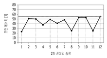
도 3 및 도 4는 각각 기판 및 도전층에 다양한 전처리를 한 경우의 표면 에너지를 나타낸 것이다.
도 5 내지 도 14는 본 발명의 실시예에 따른 액정 표시 장치의 하부 표시판의 제조 방법의 일 예를 나타낸다.
도 15 내지 도 19는 본 발명의 실시예에 따른 액정 표시 장치의 상부 표시판의 제조 방법의 일 예를 나타낸다.
| 케이스 | 전처리 종류 |
| 1 | CF4 , 30초, 수세 0회 |
| 2 | CF4 , 30초, 수세 1회 |
| 3 | CF4 , 30초, 수세 3회 |
| 4 | CF4 , 10초, 수세 0회 |
| 5 | CF4 , 10초, 수세 1회 |
| 6 | 감광제 코팅(Photoresist coating) |
| 7 | HMDS(Hexamethyl-disilzane) 1회 |
| 8 | 산 처리 |
| 9 | 염기 처리 |
| 10 | UV 처리 |
| 11 | O2 |
| 12 | 브러싱(brushing) |
빗금 표시: 2차 전처리:
x 표시: 3차 전처리
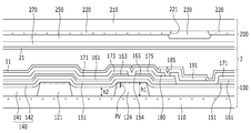
3: 액정층
11, 21: 배향막
110, 210: 기판
100, 200: 표시판
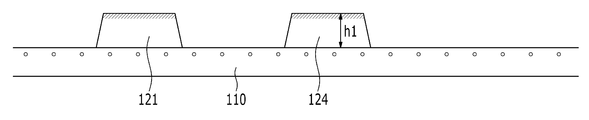
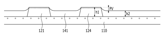
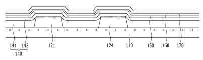
121, 124: 게이트선, 게이트 전극
140: 게이트 절연막
154: 반도체
163, 165: 저항성 접촉 부재
171, 173, 175: 데이터선, 소스 전극, 드레인 전극
180: 보호막
191: 화소 전극
220: 차광 부재
230: 색필터
250: 덮개막
270: 공통 전극
Claims (17)
상기 제1 기판 위에 형성되어 있고, 2차 전처리된 도전체; 및
상기 제1 기판 및 상기 도전체 위에 형성되어 있는 절연막
을 포함하고,
상기 1차 전처리는 상기 제1 기판의 표면 에너지가 제1 기준값보다 높아지도록 처리하는 것이고, 상기 2차 전처리는 상기 도전체의 표면 에너지가 제2 기준값보다 낮아지도록 처리하는 것을 특징으로 하는 표시 장치.
상기 제1 기준값은 상기 제1 기판에 상기 1차 전처리를 하기 전의 상기 제1 기판의 표면 에너지이고,
상기 제2 기준값은 상기 도전체에 상기 2차 전처리를 하기 전의 상기 도전체의 표면 에너지인 것을 특징으로 하는 표시 장치.
상기 1차 전처리된 상기 제1 기판의 표면 에너지는 55J 이상이고, 상기 2차 전처리된 상기 도전체의 표면 에너지는 30J 이하인 것을 특징으로 하는 표시 장치.
상기 1차 전처리는 상기 제1 기판 위에 SF6, CF4 및 O2 중 하나를 PECVD(plasma enhanced chemical vapor deposition) 방식으로 처리하는 것을 특징으로 하는 표시 장치.
상기 2차 전처리는 상기 도전체 위에 SF6, CF4 및 O2 중 하나를 PECVD 방식으로 처리하는 것을 특징으로 하는 표시 장치.
상기 절연막의 피크-밸리는 0.6um 이하인 표시 장치.
제2 기판;
제2 기판 위에 형성되어 있는 개구부를 포함하는 차광 부재; 및
상기 개구부에 형성되어 있는 색필터를 더 포함하되,
상기 개구부를 제외한 차광 부재의 표면은 상기 색필터와 반발성을 갖도록 3차 전처리된 것을 특징으로 하는 표시 장치.
상기 제1 기판 위에 도전층을 형성하는 단계;
상기 도전층의 표면 에너지가 제2 기준값보다 낮아지도록 상기 도전층에 2차 전처리를 하는 단계;
상기 도전층을 패터닝하여 도전체를 형성하는 단계; 및
상기 제1 기판 및 상기 도전체 위에 절연막을 형성하는 단계를 포함하는 것을 특징으로 하는 표시 장치의 제조 방법.
상기 제1 기준값은 상기 제1 기판에 상기 1차 전처리를 하기 전의 상기 제1 기판의 표면 에너지이고,
상기 제2 기준값은 상기 도전층에 상기 2차 전처리를 하기 전의 상기 도전층의 표면 에너지인 것을 특징으로 하는 표시 장치의 제조 방법.
상기 1차 전처리를 하는 단계는
상기 제1 기판 위에 SF6 또는 CF4를 PECVD 방식으로 10초 이상 처리하는 단계; 및
상기 제1 기판을 적어도 1회 이상 수세하는 단계
를 포함하는 것을 특징으로 하는 표시 장치의 제조 방법.
상기 2차 전처리를 하는 단계는 SF6 또는 CF4를 30초 이상 PECVD 방식으로 처리하는 것을 특징으로 하는 표시 장치의 제조 방법.
상기 절연막을 형성하는 단계는 상기 2차 전처리 후 수세 없이 상기 절연막을 형성하는 것을 특징으로 하는 표시 장치의 제조 방법.
상기 절연막을 형성하는 단계는
제1 절연막을 도포하는 단계;
상기 제1 절연막을 상기 도전체가 노출될 때까지 식각하는 단계; 및
상기 제1 절연막 위에 제2 절연막을 도포하는 단계를 포함하는 표시 장치의 제조 방법.
식각된 상기 제1 절연막의 피크-밸리는 0.6um 이하인 표시 장치의 제조 방법.
제2 기판 위에 색필터를 형성하는 단계; 및
상기 제2 기판을 상기 제1 기판과 합착하는 단계
를 더 포함하는 것을 특징으로 하는 표시 장치의 제조 방법.
상기 제2 기판 위에 상기 색필터를 형성하는 단계는
상기 제2 기판 위에 차광 부재를 도포하는 단계;
상기 차광 부재에 3차 전처리를 하는 단계;
상기 3차 전처리된 상기 차광 부재를 식각하여 복수의 개구부를 형성하는 단계; 및
상기 복수의 개구부 각각에 색물질을 잉크젯 인쇄 방식으로 도포하여 상기 색필터를 형성하는 단계
를 포함하고,
상기 3차 전처리는 상기 차광 부재가 상기 색물질과 반발성을 갖도록 처리하는 것을 특징으로 하는 표시 장치의 제조 방법.
상기 색물질은 친수성이고, 상기 3차 전처리는 상기 차광 부재가 소수성을 갖도록 하는 것을 특징으로 하는 표시 장치의 제조 방법.
Priority Applications (3)
| Application Number | Priority Date | Filing Date | Title |
|---|---|---|---|
| KR1020110027611A KR20120109856A (ko) | 2011-03-28 | 2011-03-28 | 표시 장치 및 그 제조 방법 |
| US13/211,360 US9224763B2 (en) | 2011-03-28 | 2011-08-17 | Display device and method of manufacturing the same |
| US14/950,904 US20160099263A1 (en) | 2011-03-28 | 2015-11-24 | Display device and method of manufacturing the same |
Applications Claiming Priority (1)
| Application Number | Priority Date | Filing Date | Title |
|---|---|---|---|
| KR1020110027611A KR20120109856A (ko) | 2011-03-28 | 2011-03-28 | 표시 장치 및 그 제조 방법 |
Publications (1)
| Publication Number | Publication Date |
|---|---|
| KR20120109856A true KR20120109856A (ko) | 2012-10-09 |
Family
ID=46926051
Family Applications (1)
| Application Number | Title | Priority Date | Filing Date |
|---|---|---|---|
| KR1020110027611A Abandoned KR20120109856A (ko) | 2011-03-28 | 2011-03-28 | 표시 장치 및 그 제조 방법 |
Country Status (2)
| Country | Link |
|---|---|
| US (2) | US9224763B2 (ko) |
| KR (1) | KR20120109856A (ko) |
Families Citing this family (2)
| Publication number | Priority date | Publication date | Assignee | Title |
|---|---|---|---|---|
| CN103779202B (zh) * | 2014-01-27 | 2016-12-07 | 深圳市华星光电技术有限公司 | 像素结构及其制作方法和显示面板 |
| KR102928320B1 (ko) * | 2021-09-30 | 2026-02-19 | 삼성디스플레이 주식회사 | 디스플레이 장치 및 그 제조방법 |
Family Cites Families (16)
| Publication number | Priority date | Publication date | Assignee | Title |
|---|---|---|---|---|
| JPH10229197A (ja) * | 1997-02-17 | 1998-08-25 | Sanyo Electric Co Ltd | 薄膜トランジスタ、薄膜トランジスタの製造方法 |
| TWI246633B (en) * | 1997-12-12 | 2006-01-01 | Applied Materials Inc | Method of pattern etching a low k dielectric layen |
| US6567148B1 (en) | 1998-09-10 | 2003-05-20 | Sharp Kabushiki Kaisha | Electrode substrate having particular projecting portion, manufacturing method thereof, and liquid crystal display element |
| US20070024800A1 (en) | 2003-06-04 | 2007-02-01 | Tadahiro Ohmi | Substrate and process for producing the same |
| US7575965B2 (en) | 2003-12-02 | 2009-08-18 | Semiconductor Energy Laboratory Co., Ltd. | Method for forming large area display wiring by droplet discharge, and method for manufacturing electronic device and semiconductor device |
| KR101012495B1 (ko) | 2004-06-11 | 2011-02-08 | 엘지디스플레이 주식회사 | 액정표시장치용 어레이 기판 제조 방법 |
| US8383014B2 (en) * | 2010-06-15 | 2013-02-26 | Cabot Corporation | Metal nanoparticle compositions |
| JP2007043131A (ja) | 2005-07-05 | 2007-02-15 | Tohoku Univ | 薄膜トランジスタ、配線板、及びそれらの製造方法 |
| JP2007256805A (ja) | 2006-03-24 | 2007-10-04 | Toppan Printing Co Ltd | カラーフィルタ及びその製造方法 |
| JP4222390B2 (ja) | 2006-07-25 | 2009-02-12 | セイコーエプソン株式会社 | パターンの形成方法、及び液晶表示装置の製造方法 |
| JP2008066567A (ja) | 2006-09-08 | 2008-03-21 | Ricoh Co Ltd | 配線パターンとこれを用いた電子素子、有機半導体素子、積層配線パターンおよび積層配線基板 |
| CA2682928A1 (en) * | 2007-04-19 | 2008-10-30 | Basf Se | Method for forming a pattern on a substrate and electronic device formed thereby |
| JP2009026900A (ja) | 2007-07-18 | 2009-02-05 | Ricoh Co Ltd | 積層構造体、電子素子及びそれらの製造方法、表示装置 |
| JP5436101B2 (ja) * | 2008-09-05 | 2014-03-05 | 株式会社半導体エネルギー研究所 | 半導体装置の作製方法 |
| KR101287478B1 (ko) * | 2009-06-02 | 2013-07-19 | 엘지디스플레이 주식회사 | 산화물 박막트랜지스터를 구비한 표시소자 및 그 제조방법 |
| KR102192753B1 (ko) * | 2010-03-08 | 2020-12-18 | 가부시키가이샤 한도오따이 에네루기 켄큐쇼 | 반도체 장치 및 반도체 장치를 제작하는 방법 |
-
2011
- 2011-03-28 KR KR1020110027611A patent/KR20120109856A/ko not_active Abandoned
- 2011-08-17 US US13/211,360 patent/US9224763B2/en active Active
-
2015
- 2015-11-24 US US14/950,904 patent/US20160099263A1/en not_active Abandoned
Also Published As
| Publication number | Publication date |
|---|---|
| US20160099263A1 (en) | 2016-04-07 |
| US20120248480A1 (en) | 2012-10-04 |
| US9224763B2 (en) | 2015-12-29 |
Similar Documents
| Publication | Publication Date | Title |
|---|---|---|
| KR101525805B1 (ko) | 표시 장치 및 그 제조 방법 | |
| US8610871B2 (en) | Method for forming multilayer structure, method for manufacturing display panel, and display panel | |
| CN1469174A (zh) | 具有滤色器阵列衬底的液晶显示器件及其制造方法 | |
| US20080227242A1 (en) | Pixel structure of a thin film transistor liquid crystal display | |
| KR20030048489A (ko) | 횡전계형 액정표시장치 | |
| US7602452B2 (en) | Liquid crystal display device and method for manufacturing the same | |
| KR101472849B1 (ko) | 박막트랜지스터 기판, 이의 제조 방법 및 이를 갖는액정표시패널 | |
| KR20040043864A (ko) | 박막 트랜지스터 어레이 기판 및 그 제조 방법 | |
| KR20100005457A (ko) | 박막 트랜지스터 표시판 및 이의 제조 방법 | |
| KR20100005454A (ko) | 박막 트랜지스터 표시판 및 그 제조 방법 | |
| KR101479997B1 (ko) | 액정 표시 장치 및 그 제조 방법 | |
| KR101270705B1 (ko) | 박막 트랜지스터 기판과 이의 제조 방법 및 이를 구비한액정표시패널 | |
| KR20120097696A (ko) | 박막 트랜지스터 표시판 및 그 제조 방법 | |
| KR20100031378A (ko) | 박막 트랜지스터 기판 및 이의 제조 방법 | |
| KR20080053541A (ko) | 박막 트랜지스터 기판 및 이의 제조 방법 | |
| CN111679517A (zh) | 一种显示面板及其制造方法,显示装置 | |
| US8304772B2 (en) | Thin-film transistor array panel and method of fabricating the same | |
| US7525624B2 (en) | Liquid crystal display device and fabricating method thereof | |
| KR20120109856A (ko) | 표시 장치 및 그 제조 방법 | |
| KR20030055938A (ko) | 액정표시소자 및 그 제조방법 | |
| US8866198B2 (en) | Display device and method for manufacturing the same | |
| US10895786B2 (en) | Liquid crystal display device and method of manufacturing the same | |
| KR101032603B1 (ko) | 액정표시장치용 어레이기판 제조방법 | |
| KR102390430B1 (ko) | 액정 표시 장치 및 그의 제조 방법 | |
| KR20110017785A (ko) | 박막 트랜지스터 표시판 및 그 제조 방법 |
Legal Events
| Date | Code | Title | Description |
|---|---|---|---|
| PA0109 | Patent application |
Patent event code: PA01091R01D Comment text: Patent Application Patent event date: 20110328 |
|
| N231 | Notification of change of applicant | ||
| PN2301 | Change of applicant |
Patent event date: 20120913 Comment text: Notification of Change of Applicant Patent event code: PN23011R01D |
|
| PG1501 | Laying open of application | ||
| A201 | Request for examination | ||
| PA0201 | Request for examination |
Patent event code: PA02012R01D Patent event date: 20160302 Comment text: Request for Examination of Application Patent event code: PA02011R01I Patent event date: 20110328 Comment text: Patent Application |
|
| E902 | Notification of reason for refusal | ||
| PE0902 | Notice of grounds for rejection |
Comment text: Notification of reason for refusal Patent event date: 20170118 Patent event code: PE09021S01D |
|
| E701 | Decision to grant or registration of patent right | ||
| PE0701 | Decision of registration |
Patent event code: PE07011S01D Comment text: Decision to Grant Registration Patent event date: 20170630 |
|
| NORF | Unpaid initial registration fee | ||
| PC1904 | Unpaid initial registration fee |