KR20120132931A - 발광소자패키지 - Google Patents
발광소자패키지 Download PDFInfo
- Publication number
- KR20120132931A KR20120132931A KR20110051340A KR20110051340A KR20120132931A KR 20120132931 A KR20120132931 A KR 20120132931A KR 20110051340 A KR20110051340 A KR 20110051340A KR 20110051340 A KR20110051340 A KR 20110051340A KR 20120132931 A KR20120132931 A KR 20120132931A
- Authority
- KR
- South Korea
- Prior art keywords
- light emitting
- emitting device
- wire
- lead frame
- device package
- Prior art date
- Legal status (The legal status is an assumption and is not a legal conclusion. Google has not performed a legal analysis and makes no representation as to the accuracy of the status listed.)
- Granted
Links
Images



Classifications
-
- H—ELECTRICITY
- H10—SEMICONDUCTOR DEVICES; ELECTRIC SOLID-STATE DEVICES NOT OTHERWISE PROVIDED FOR
- H10H—INORGANIC LIGHT-EMITTING SEMICONDUCTOR DEVICES HAVING POTENTIAL BARRIERS
- H10H20/00—Individual inorganic light-emitting semiconductor devices having potential barriers, e.g. light-emitting diodes [LED]
- H10H20/80—Constructional details
- H10H20/85—Packages
- H10H20/857—Interconnections, e.g. lead-frames, bond wires or solder balls
-
- H—ELECTRICITY
- H10—SEMICONDUCTOR DEVICES; ELECTRIC SOLID-STATE DEVICES NOT OTHERWISE PROVIDED FOR
- H10H—INORGANIC LIGHT-EMITTING SEMICONDUCTOR DEVICES HAVING POTENTIAL BARRIERS
- H10H20/00—Individual inorganic light-emitting semiconductor devices having potential barriers, e.g. light-emitting diodes [LED]
- H10H20/01—Manufacture or treatment
- H10H20/036—Manufacture or treatment of packages
- H10H20/0364—Manufacture or treatment of packages of interconnections
-
- F—MECHANICAL ENGINEERING; LIGHTING; HEATING; WEAPONS; BLASTING
- F21—LIGHTING
- F21K—NON-ELECTRIC LIGHT SOURCES USING LUMINESCENCE; LIGHT SOURCES USING ELECTROCHEMILUMINESCENCE; LIGHT SOURCES USING CHARGES OF COMBUSTIBLE MATERIAL; LIGHT SOURCES USING SEMICONDUCTOR DEVICES AS LIGHT-GENERATING ELEMENTS; LIGHT SOURCES NOT OTHERWISE PROVIDED FOR
- F21K9/00—Light sources using semiconductor devices as light-generating elements, e.g. using light-emitting diodes [LED] or lasers
- F21K9/20—Light sources comprising attachment means
- F21K9/27—Retrofit light sources for lighting devices with two fittings for each light source, e.g. for substitution of fluorescent tubes
-
- F—MECHANICAL ENGINEERING; LIGHTING; HEATING; WEAPONS; BLASTING
- F21—LIGHTING
- F21Y—INDEXING SCHEME ASSOCIATED WITH SUBCLASSES F21K, F21L, F21S and F21V, RELATING TO THE FORM OR THE KIND OF THE LIGHT SOURCES OR OF THE COLOUR OF THE LIGHT EMITTED
- F21Y2113/00—Combination of light sources
- F21Y2113/10—Combination of light sources of different colours
- F21Y2113/13—Combination of light sources of different colours comprising an assembly of point-like light sources
-
- F—MECHANICAL ENGINEERING; LIGHTING; HEATING; WEAPONS; BLASTING
- F21—LIGHTING
- F21Y—INDEXING SCHEME ASSOCIATED WITH SUBCLASSES F21K, F21L, F21S and F21V, RELATING TO THE FORM OR THE KIND OF THE LIGHT SOURCES OR OF THE COLOUR OF THE LIGHT EMITTED
- F21Y2115/00—Light-generating elements of semiconductor light sources
- F21Y2115/10—Light-emitting diodes [LED]
-
- H—ELECTRICITY
- H10—SEMICONDUCTOR DEVICES; ELECTRIC SOLID-STATE DEVICES NOT OTHERWISE PROVIDED FOR
- H10W—GENERIC PACKAGES, INTERCONNECTIONS, CONNECTORS OR OTHER CONSTRUCTIONAL DETAILS OF DEVICES COVERED BY CLASS H10
- H10W72/00—Interconnections or connectors in packages
- H10W72/50—Bond wires
- H10W72/531—Shapes of wire connectors
- H10W72/536—Shapes of wire connectors the connected ends being ball-shaped
-
- H—ELECTRICITY
- H10—SEMICONDUCTOR DEVICES; ELECTRIC SOLID-STATE DEVICES NOT OTHERWISE PROVIDED FOR
- H10W—GENERIC PACKAGES, INTERCONNECTIONS, CONNECTORS OR OTHER CONSTRUCTIONAL DETAILS OF DEVICES COVERED BY CLASS H10
- H10W72/00—Interconnections or connectors in packages
- H10W72/50—Bond wires
- H10W72/531—Shapes of wire connectors
- H10W72/5363—Shapes of wire connectors the connected ends being wedge-shaped
-
- H—ELECTRICITY
- H10—SEMICONDUCTOR DEVICES; ELECTRIC SOLID-STATE DEVICES NOT OTHERWISE PROVIDED FOR
- H10W—GENERIC PACKAGES, INTERCONNECTIONS, CONNECTORS OR OTHER CONSTRUCTIONAL DETAILS OF DEVICES COVERED BY CLASS H10
- H10W72/00—Interconnections or connectors in packages
- H10W72/50—Bond wires
- H10W72/541—Dispositions of bond wires
- H10W72/5434—Dispositions of bond wires the connected ends being on auxiliary connecting means on bond pads, e.g. on other bond wires
-
- H—ELECTRICITY
- H10—SEMICONDUCTOR DEVICES; ELECTRIC SOLID-STATE DEVICES NOT OTHERWISE PROVIDED FOR
- H10W—GENERIC PACKAGES, INTERCONNECTIONS, CONNECTORS OR OTHER CONSTRUCTIONAL DETAILS OF DEVICES COVERED BY CLASS H10
- H10W72/00—Interconnections or connectors in packages
- H10W72/50—Bond wires
- H10W72/541—Dispositions of bond wires
- H10W72/547—Dispositions of multiple bond wires
- H10W72/5473—Dispositions of multiple bond wires multiple bond wires connected to a common bond pad
-
- H—ELECTRICITY
- H10—SEMICONDUCTOR DEVICES; ELECTRIC SOLID-STATE DEVICES NOT OTHERWISE PROVIDED FOR
- H10W—GENERIC PACKAGES, INTERCONNECTIONS, CONNECTORS OR OTHER CONSTRUCTIONAL DETAILS OF DEVICES COVERED BY CLASS H10
- H10W72/00—Interconnections or connectors in packages
- H10W72/50—Bond wires
- H10W72/551—Materials of bond wires
- H10W72/552—Materials of bond wires comprising metals or metalloids, e.g. silver
-
- H—ELECTRICITY
- H10—SEMICONDUCTOR DEVICES; ELECTRIC SOLID-STATE DEVICES NOT OTHERWISE PROVIDED FOR
- H10W—GENERIC PACKAGES, INTERCONNECTIONS, CONNECTORS OR OTHER CONSTRUCTIONAL DETAILS OF DEVICES COVERED BY CLASS H10
- H10W72/00—Interconnections or connectors in packages
- H10W72/50—Bond wires
- H10W72/551—Materials of bond wires
- H10W72/552—Materials of bond wires comprising metals or metalloids, e.g. silver
- H10W72/5522—Materials of bond wires comprising metals or metalloids, e.g. silver comprising gold [Au]
-
- H—ELECTRICITY
- H10—SEMICONDUCTOR DEVICES; ELECTRIC SOLID-STATE DEVICES NOT OTHERWISE PROVIDED FOR
- H10W—GENERIC PACKAGES, INTERCONNECTIONS, CONNECTORS OR OTHER CONSTRUCTIONAL DETAILS OF DEVICES COVERED BY CLASS H10
- H10W72/00—Interconnections or connectors in packages
- H10W72/50—Bond wires
- H10W72/551—Materials of bond wires
- H10W72/552—Materials of bond wires comprising metals or metalloids, e.g. silver
- H10W72/5524—Materials of bond wires comprising metals or metalloids, e.g. silver comprising aluminium [Al]
-
- H—ELECTRICITY
- H10—SEMICONDUCTOR DEVICES; ELECTRIC SOLID-STATE DEVICES NOT OTHERWISE PROVIDED FOR
- H10W—GENERIC PACKAGES, INTERCONNECTIONS, CONNECTORS OR OTHER CONSTRUCTIONAL DETAILS OF DEVICES COVERED BY CLASS H10
- H10W72/00—Interconnections or connectors in packages
- H10W72/50—Bond wires
- H10W72/551—Materials of bond wires
- H10W72/552—Materials of bond wires comprising metals or metalloids, e.g. silver
- H10W72/5525—Materials of bond wires comprising metals or metalloids, e.g. silver comprising copper [Cu]
-
- H—ELECTRICITY
- H10—SEMICONDUCTOR DEVICES; ELECTRIC SOLID-STATE DEVICES NOT OTHERWISE PROVIDED FOR
- H10W—GENERIC PACKAGES, INTERCONNECTIONS, CONNECTORS OR OTHER CONSTRUCTIONAL DETAILS OF DEVICES COVERED BY CLASS H10
- H10W72/00—Interconnections or connectors in packages
- H10W72/50—Bond wires
- H10W72/581—Auxiliary members, e.g. flow barriers
- H10W72/583—Reinforcing structures
-
- H—ELECTRICITY
- H10—SEMICONDUCTOR DEVICES; ELECTRIC SOLID-STATE DEVICES NOT OTHERWISE PROVIDED FOR
- H10W—GENERIC PACKAGES, INTERCONNECTIONS, CONNECTORS OR OTHER CONSTRUCTIONAL DETAILS OF DEVICES COVERED BY CLASS H10
- H10W72/00—Interconnections or connectors in packages
- H10W72/90—Bond pads, in general
- H10W72/951—Materials of bond pads
- H10W72/952—Materials of bond pads comprising metals or metalloids, e.g. PbSn, Ag or Cu
-
- H—ELECTRICITY
- H10—SEMICONDUCTOR DEVICES; ELECTRIC SOLID-STATE DEVICES NOT OTHERWISE PROVIDED FOR
- H10W—GENERIC PACKAGES, INTERCONNECTIONS, CONNECTORS OR OTHER CONSTRUCTIONAL DETAILS OF DEVICES COVERED BY CLASS H10
- H10W74/00—Encapsulations, e.g. protective coatings
-
- H—ELECTRICITY
- H10—SEMICONDUCTOR DEVICES; ELECTRIC SOLID-STATE DEVICES NOT OTHERWISE PROVIDED FOR
- H10W—GENERIC PACKAGES, INTERCONNECTIONS, CONNECTORS OR OTHER CONSTRUCTIONAL DETAILS OF DEVICES COVERED BY CLASS H10
- H10W90/00—Package configurations
-
- H—ELECTRICITY
- H10—SEMICONDUCTOR DEVICES; ELECTRIC SOLID-STATE DEVICES NOT OTHERWISE PROVIDED FOR
- H10W—GENERIC PACKAGES, INTERCONNECTIONS, CONNECTORS OR OTHER CONSTRUCTIONAL DETAILS OF DEVICES COVERED BY CLASS H10
- H10W90/00—Package configurations
- H10W90/701—Package configurations characterised by the relative positions of pads or connectors relative to package parts
- H10W90/751—Package configurations characterised by the relative positions of pads or connectors relative to package parts of bond wires
- H10W90/756—Package configurations characterised by the relative positions of pads or connectors relative to package parts of bond wires between a chip and a stacked lead frame, conducting package substrate or heat sink
Landscapes
- Led Device Packages (AREA)
Abstract
Description
도 2는 실시예에 따른 발광소자 패키지의 와이어 본딩구조를 나타내는 도이다.
도 3a 및 도 3b는 실시예에 따른 발광소자 패키지의 와이어 본딩구조를 나타내는 도이다.
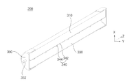
도 4a는 실시예에 따른 발광소자패키지를 포함하는 조명장치를 도시한 사시도이며, 도 4b는 도 4a의 조명장치의 D-D' 단면을 도시한 단면도이다.
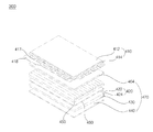
도 5은 실시예에 따른 발광소자패키지를 포함하는 백라이트 유닛을 도시한 분해 사시도이다.
도 6은 실시예에 따른 발광소자패키지를 포함하는 백라이트 유닛을 도시한 분해 사시도이다.
120 : 리드프레임 130: 발광소자
140: 수지물 150: 전극패드
160 : 패드볼 170, 270: 제1 와이어
175, 275: 제2 와이어 180, 280: 제1 접점
185, 285: 제2 접점 190, 290: 제1 접합볼
195, 295: 제2 접합볼
Claims (11)
- 제1 리드프레임 상에 위치하고, 상면에 전극패드를 구비하는 발광소자;
상기 제1 리드프레임과 이격되어 위치하는 제2 리드프레임과 상기 전극패드를 전기적으로 연결하는 제1 와이어; 및
상기 제2 리드프레임 상에서, 상기 제1 와이어와 상기 제2 리드프레임이 접하는 제1 접점과 이격되어 위치하는 제1 접합볼을 포함하고,
상기 제1 접합볼은 상기 제1 와이어와 상기 제2 리드프레임 사이에 위치하여, 상기 제1 와이어와 상기 제2 리드프레임을 전기적으로 연결하는 발광소자 패키지. - 제1항에 있어서,
상기 발광소자는 상기 전극패드 상에 패드볼을 포함하고,
상기 제1 와이어는 상기 패드볼과 상기 제2 리드프레임을 전기적으로 연결하는 발광소자 패키지. - 제1항에 있어서,
상기 제1 접합볼 상에는 제2 접합볼을 포함하고,
상기 제1 와이어는 상기 제1 접합볼과 상기 제2 접합볼 사이에 위치하여, 상기 제1 접합볼과 상기 제2 접합볼은 상기 제1 와이어를 고정하는 발광소자 패키지. - 제3항에 있어서,
상기 제1 접합볼 또는 상기 제2 접합볼 중 어느 하나와 상기 제2 리드프레임을 전기적으로 연결하는 제2 와이어를 포함하는 발광소자 패키지. - 제4항에 있어서,
상기 제2 와이어와 상기 제2 리드프레임이 접하는 제2 접점은 상기 제1 접점과 이격되어 위치하는 발광소자 패키지. - 제1항에 있어서,
상기 제1 접점 상에 접착제가 도포된 발광소자 패키지. - 제1항 또는 제3항에 있어서,
상기 제1 접합볼 또는 상기 제2 접합볼은 Ag로 이루어진 발광소자 패키지. - 제1항에 있어서,
상기 발광소자가 실장되는 캐비티가 형성된 패키지 몸체 및
상기 캐비티에 충진된 수지물을 포함하는 발광소자 패키지. - 제8항에 있어서,
상기 수지물은 형광체 및 광확산재 중 적어도 하나를 포함하는 발광소자 패키지. - 제1항 내지 제9항 중 어느 한 항의 발광소자패키지를 포함하는 조명장치.
- 제1항 내지 제9항 중 어느 한 항의 발광소자패키지를 포함하는 백라이트 장치.
Priority Applications (4)
| Application Number | Priority Date | Filing Date | Title |
|---|---|---|---|
| KR1020110051340A KR101805118B1 (ko) | 2011-05-30 | 2011-05-30 | 발광소자패키지 |
| US13/412,024 US8492786B2 (en) | 2011-05-30 | 2012-03-05 | Light emitting device package and lighting system |
| EP12158521.0A EP2530754B1 (en) | 2011-05-30 | 2012-03-08 | Light emitting device package and lighting system |
| CN201210083699.3A CN102810623B (zh) | 2011-05-30 | 2012-03-27 | 发光器件封装和照明系统 |
Applications Claiming Priority (1)
| Application Number | Priority Date | Filing Date | Title |
|---|---|---|---|
| KR1020110051340A KR101805118B1 (ko) | 2011-05-30 | 2011-05-30 | 발광소자패키지 |
Publications (2)
| Publication Number | Publication Date |
|---|---|
| KR20120132931A true KR20120132931A (ko) | 2012-12-10 |
| KR101805118B1 KR101805118B1 (ko) | 2017-12-05 |
Family
ID=45787124
Family Applications (1)
| Application Number | Title | Priority Date | Filing Date |
|---|---|---|---|
| KR1020110051340A Expired - Fee Related KR101805118B1 (ko) | 2011-05-30 | 2011-05-30 | 발광소자패키지 |
Country Status (4)
| Country | Link |
|---|---|
| US (1) | US8492786B2 (ko) |
| EP (1) | EP2530754B1 (ko) |
| KR (1) | KR101805118B1 (ko) |
| CN (1) | CN102810623B (ko) |
Families Citing this family (10)
| Publication number | Priority date | Publication date | Assignee | Title |
|---|---|---|---|---|
| KR102007404B1 (ko) * | 2012-12-14 | 2019-08-05 | 엘지이노텍 주식회사 | 발광소자 패키지 |
| US20140209950A1 (en) * | 2013-01-31 | 2014-07-31 | Luxo-Led Co., Limited | Light emitting diode package module |
| JP6136701B2 (ja) * | 2013-07-24 | 2017-05-31 | 日亜化学工業株式会社 | 発光装置 |
| KR20150025231A (ko) * | 2013-08-28 | 2015-03-10 | 서울반도체 주식회사 | 광원 모듈 및 그 제조 방법, 및 백라이트 유닛 |
| CN103972221A (zh) * | 2014-06-03 | 2014-08-06 | 宁波升谱光电半导体有限公司 | Led光源封装结构及led光源封装方法 |
| CN107045992A (zh) * | 2017-04-19 | 2017-08-15 | 中国科学院上海微系统与信息技术研究所 | 图像传感器圆片级封装方法及封装结构 |
| US10622531B2 (en) | 2017-09-28 | 2020-04-14 | Nichia Corporation | Light-emitting device |
| JP7174218B2 (ja) * | 2017-12-27 | 2022-11-17 | 日亜化学工業株式会社 | 発光装置及びその製造方法 |
| CN108506798A (zh) * | 2018-03-20 | 2018-09-07 | 京东方科技集团股份有限公司 | 显示装置及侧入式光源模组 |
| CN113035817A (zh) * | 2019-12-25 | 2021-06-25 | 上海凯虹科技电子有限公司 | 一种封装体 |
Family Cites Families (10)
| Publication number | Priority date | Publication date | Assignee | Title |
|---|---|---|---|---|
| JPS5230231B2 (ko) * | 1973-03-26 | 1977-08-06 | ||
| JP3869562B2 (ja) | 1998-10-16 | 2007-01-17 | 三洋電機株式会社 | 半導体装置の製造方法 |
| JP2001015541A (ja) * | 1999-06-28 | 2001-01-19 | Sumitomo Electric Ind Ltd | 半導体装置および半導体装置の製造方法 |
| JP2003197669A (ja) * | 2001-12-28 | 2003-07-11 | Seiko Epson Corp | ボンディング方法及びボンディング装置 |
| JP3888438B2 (ja) * | 2002-02-25 | 2007-03-07 | セイコーエプソン株式会社 | 半導体装置及びその製造方法、回路基板並びに電子機器 |
| US20030230796A1 (en) | 2002-06-12 | 2003-12-18 | Aminuddin Ismail | Stacked die semiconductor device |
| CN100347867C (zh) * | 2004-02-26 | 2007-11-07 | 元砷光电科技股份有限公司 | 发光二极管的焊球制造工艺 |
| JP5008832B2 (ja) * | 2005-04-15 | 2012-08-22 | ローム株式会社 | 半導体装置及び半導体装置の製造方法 |
| US7476608B2 (en) * | 2005-07-14 | 2009-01-13 | Hewlett-Packard Development Company, L.P. | Electrically connecting substrate with electrical device |
| KR101488448B1 (ko) * | 2007-12-06 | 2015-02-02 | 서울반도체 주식회사 | Led 패키지 및 그 제조방법 |
-
2011
- 2011-05-30 KR KR1020110051340A patent/KR101805118B1/ko not_active Expired - Fee Related
-
2012
- 2012-03-05 US US13/412,024 patent/US8492786B2/en active Active
- 2012-03-08 EP EP12158521.0A patent/EP2530754B1/en active Active
- 2012-03-27 CN CN201210083699.3A patent/CN102810623B/zh active Active
Also Published As
| Publication number | Publication date |
|---|---|
| CN102810623A (zh) | 2012-12-05 |
| EP2530754A2 (en) | 2012-12-05 |
| US20120305962A1 (en) | 2012-12-06 |
| CN102810623B (zh) | 2017-03-01 |
| KR101805118B1 (ko) | 2017-12-05 |
| EP2530754B1 (en) | 2016-12-21 |
| EP2530754A3 (en) | 2015-02-25 |
| US8492786B2 (en) | 2013-07-23 |
Similar Documents
| Publication | Publication Date | Title |
|---|---|---|
| KR101805118B1 (ko) | 발광소자패키지 | |
| EP2346103A2 (en) | Light emitting device and backlight unit | |
| KR101941512B1 (ko) | 발광소자 패키지 | |
| KR20120056543A (ko) | 발광소자 패키지 | |
| KR101849126B1 (ko) | 발광소자 패키지 | |
| KR102075522B1 (ko) | 발광소자패키지 | |
| KR101781047B1 (ko) | 발광 소자 패키지 | |
| KR102042208B1 (ko) | 인쇄회로기판 | |
| KR20140099073A (ko) | 발광소자 패키지 | |
| KR20120071150A (ko) | 발광 소자 패키지 | |
| KR101911939B1 (ko) | 발광소자 패키지 | |
| KR101978941B1 (ko) | 발광소자 패키지 | |
| KR101831278B1 (ko) | 발광소자 패키지 | |
| KR101894933B1 (ko) | 발광소자 패키지 | |
| KR20130061421A (ko) | 발광소자 패키지 | |
| KR101722622B1 (ko) | 발광소자 패키지 | |
| KR20120073929A (ko) | 발광소자 패키지 | |
| KR20120071151A (ko) | 발광소자 패키지 | |
| KR101883344B1 (ko) | 발광소자 어레이 | |
| KR20120072737A (ko) | 발광 소자 패키지 | |
| KR20130014899A (ko) | 발광소자 패키지 | |
| KR20120034484A (ko) | 발광소자 패키지 | |
| KR20120109732A (ko) | 발광소자 패키지 및 조명시스템 | |
| KR20120087581A (ko) | 발광소자 패키지 | |
| KR20120014490A (ko) | 리드 프레임을 포함하는 발광소자 패키지 |
Legal Events
| Date | Code | Title | Description |
|---|---|---|---|
| PA0109 | Patent application |
St.27 status event code: A-0-1-A10-A12-nap-PA0109 |
|
| PG1501 | Laying open of application |
St.27 status event code: A-1-1-Q10-Q12-nap-PG1501 |
|
| PN2301 | Change of applicant |
St.27 status event code: A-3-3-R10-R13-asn-PN2301 St.27 status event code: A-3-3-R10-R11-asn-PN2301 |
|
| A201 | Request for examination | ||
| PA0201 | Request for examination |
St.27 status event code: A-1-2-D10-D11-exm-PA0201 |
|
| E13-X000 | Pre-grant limitation requested |
St.27 status event code: A-2-3-E10-E13-lim-X000 |
|
| P11-X000 | Amendment of application requested |
St.27 status event code: A-2-2-P10-P11-nap-X000 |
|
| P13-X000 | Application amended |
St.27 status event code: A-2-2-P10-P13-nap-X000 |
|
| E902 | Notification of reason for refusal | ||
| PE0902 | Notice of grounds for rejection |
St.27 status event code: A-1-2-D10-D21-exm-PE0902 |
|
| R18-X000 | Changes to party contact information recorded |
St.27 status event code: A-3-3-R10-R18-oth-X000 |
|
| E13-X000 | Pre-grant limitation requested |
St.27 status event code: A-2-3-E10-E13-lim-X000 |
|
| P11-X000 | Amendment of application requested |
St.27 status event code: A-2-2-P10-P11-nap-X000 |
|
| P13-X000 | Application amended |
St.27 status event code: A-2-2-P10-P13-nap-X000 |
|
| E701 | Decision to grant or registration of patent right | ||
| PE0701 | Decision of registration |
St.27 status event code: A-1-2-D10-D22-exm-PE0701 |
|
| GRNT | Written decision to grant | ||
| PR0701 | Registration of establishment |
St.27 status event code: A-2-4-F10-F11-exm-PR0701 |
|
| PR1002 | Payment of registration fee |
St.27 status event code: A-2-2-U10-U11-oth-PR1002 Fee payment year number: 1 |
|
| PG1601 | Publication of registration |
St.27 status event code: A-4-4-Q10-Q13-nap-PG1601 |
|
| R18-X000 | Changes to party contact information recorded |
St.27 status event code: A-5-5-R10-R18-oth-X000 |
|
| R18-X000 | Changes to party contact information recorded |
St.27 status event code: A-5-5-R10-R18-oth-X000 |
|
| FPAY | Annual fee payment |
Payment date: 20201013 Year of fee payment: 4 |
|
| PR1001 | Payment of annual fee |
St.27 status event code: A-4-4-U10-U11-oth-PR1001 Fee payment year number: 4 |
|
| PN2301 | Change of applicant |
St.27 status event code: A-5-5-R10-R13-asn-PN2301 St.27 status event code: A-5-5-R10-R11-asn-PN2301 |
|
| PN2301 | Change of applicant |
St.27 status event code: A-5-5-R10-R11-asn-PN2301 |
|
| PN2301 | Change of applicant |
St.27 status event code: A-5-5-R10-R14-asn-PN2301 |
|
| FPAY | Annual fee payment |
Payment date: 20211105 Year of fee payment: 5 |
|
| PR1001 | Payment of annual fee |
St.27 status event code: A-4-4-U10-U11-oth-PR1001 Fee payment year number: 5 |
|
| FPAY | Annual fee payment |
Payment date: 20221007 Year of fee payment: 6 |
|
| PR1001 | Payment of annual fee |
St.27 status event code: A-4-4-U10-U11-oth-PR1001 Fee payment year number: 6 |
|
| PR1001 | Payment of annual fee |
St.27 status event code: A-4-4-U10-U11-oth-PR1001 Fee payment year number: 7 |
|
| PC1903 | Unpaid annual fee |
St.27 status event code: A-4-4-U10-U13-oth-PC1903 Not in force date: 20241130 Payment event data comment text: Termination Category : DEFAULT_OF_REGISTRATION_FEE |
|
| P22-X000 | Classification modified |
St.27 status event code: A-4-4-P10-P22-nap-X000 |
|
| H13 | Ip right lapsed |
Free format text: ST27 STATUS EVENT CODE: N-4-6-H10-H13-OTH-PC1903 (AS PROVIDED BY THE NATIONAL OFFICE); TERMINATION CATEGORY : DEFAULT_OF_REGISTRATION_FEE Effective date: 20241130 |
|
| PC1903 | Unpaid annual fee |
St.27 status event code: N-4-6-H10-H13-oth-PC1903 Ip right cessation event data comment text: Termination Category : DEFAULT_OF_REGISTRATION_FEE Not in force date: 20241130 |