KR20130008100A - 유기 발광 조명 장치 - Google Patents
유기 발광 조명 장치 Download PDFInfo
- Publication number
- KR20130008100A KR20130008100A KR1020110060883A KR20110060883A KR20130008100A KR 20130008100 A KR20130008100 A KR 20130008100A KR 1020110060883 A KR1020110060883 A KR 1020110060883A KR 20110060883 A KR20110060883 A KR 20110060883A KR 20130008100 A KR20130008100 A KR 20130008100A
- Authority
- KR
- South Korea
- Prior art keywords
- light emitting
- thickness
- organic light
- thickness portion
- emitting element
- Prior art date
- Legal status (The legal status is an assumption and is not a legal conclusion. Google has not performed a legal analysis and makes no representation as to the accuracy of the status listed.)
- Ceased
Links
Images



Classifications
-
- H—ELECTRICITY
- H10—SEMICONDUCTOR DEVICES; ELECTRIC SOLID-STATE DEVICES NOT OTHERWISE PROVIDED FOR
- H10K—ORGANIC ELECTRIC SOLID-STATE DEVICES
- H10K59/00—Integrated devices, or assemblies of multiple devices, comprising at least one organic light-emitting element covered by group H10K50/00
- H10K59/80—Constructional details
- H10K59/87—Passivation; Containers; Encapsulations
- H10K59/871—Self-supporting sealing arrangements
-
- H—ELECTRICITY
- H10—SEMICONDUCTOR DEVICES; ELECTRIC SOLID-STATE DEVICES NOT OTHERWISE PROVIDED FOR
- H10K—ORGANIC ELECTRIC SOLID-STATE DEVICES
- H10K50/00—Organic light-emitting devices
- H10K50/80—Constructional details
- H10K50/84—Passivation; Containers; Encapsulations
- H10K50/841—Self-supporting sealing arrangements
-
- H—ELECTRICITY
- H10—SEMICONDUCTOR DEVICES; ELECTRIC SOLID-STATE DEVICES NOT OTHERWISE PROVIDED FOR
- H10K—ORGANIC ELECTRIC SOLID-STATE DEVICES
- H10K59/00—Integrated devices, or assemblies of multiple devices, comprising at least one organic light-emitting element covered by group H10K50/00
- H10K59/80—Constructional details
- H10K59/87—Passivation; Containers; Encapsulations
- H10K59/871—Self-supporting sealing arrangements
- H10K59/8721—Metallic sealing arrangements
-
- H—ELECTRICITY
- H10—SEMICONDUCTOR DEVICES; ELECTRIC SOLID-STATE DEVICES NOT OTHERWISE PROVIDED FOR
- H10K—ORGANIC ELECTRIC SOLID-STATE DEVICES
- H10K59/00—Integrated devices, or assemblies of multiple devices, comprising at least one organic light-emitting element covered by group H10K50/00
- H10K59/80—Constructional details
- H10K59/87—Passivation; Containers; Encapsulations
- H10K59/871—Self-supporting sealing arrangements
- H10K59/8722—Peripheral sealing arrangements, e.g. adhesives, sealants
-
- H—ELECTRICITY
- H10—SEMICONDUCTOR DEVICES; ELECTRIC SOLID-STATE DEVICES NOT OTHERWISE PROVIDED FOR
- H10K—ORGANIC ELECTRIC SOLID-STATE DEVICES
- H10K59/00—Integrated devices, or assemblies of multiple devices, comprising at least one organic light-emitting element covered by group H10K50/00
- H10K59/80—Constructional details
- H10K59/87—Passivation; Containers; Encapsulations
- H10K59/873—Encapsulations
-
- H—ELECTRICITY
- H10—SEMICONDUCTOR DEVICES; ELECTRIC SOLID-STATE DEVICES NOT OTHERWISE PROVIDED FOR
- H10K—ORGANIC ELECTRIC SOLID-STATE DEVICES
- H10K2102/00—Constructional details relating to the organic devices covered by this subclass
- H10K2102/301—Details of OLEDs
- H10K2102/351—Thickness
-
- H—ELECTRICITY
- H10—SEMICONDUCTOR DEVICES; ELECTRIC SOLID-STATE DEVICES NOT OTHERWISE PROVIDED FOR
- H10K—ORGANIC ELECTRIC SOLID-STATE DEVICES
- H10K50/00—Organic light-emitting devices
- H10K50/80—Constructional details
- H10K50/84—Passivation; Containers; Encapsulations
- H10K50/842—Containers
- H10K50/8423—Metallic sealing arrangements
-
- Y—GENERAL TAGGING OF NEW TECHNOLOGICAL DEVELOPMENTS; GENERAL TAGGING OF CROSS-SECTIONAL TECHNOLOGIES SPANNING OVER SEVERAL SECTIONS OF THE IPC; TECHNICAL SUBJECTS COVERED BY FORMER USPC CROSS-REFERENCE ART COLLECTIONS [XRACs] AND DIGESTS
- Y02—TECHNOLOGIES OR APPLICATIONS FOR MITIGATION OR ADAPTATION AGAINST CLIMATE CHANGE
- Y02B—CLIMATE CHANGE MITIGATION TECHNOLOGIES RELATED TO BUILDINGS, e.g. HOUSING, HOUSE APPLIANCES OR RELATED END-USER APPLICATIONS
- Y02B20/00—Energy efficient lighting technologies, e.g. halogen lamps or gas discharge lamps
- Y02B20/30—Semiconductor lamps, e.g. solid state lamps [SSL] light emitting diodes [LED] or organic LED [OLED]
Landscapes
- Physics & Mathematics (AREA)
- Optics & Photonics (AREA)
- Electroluminescent Light Sources (AREA)
Abstract
Description
도 2는 도 1의 유기 발광 조명 장치의 봉지캔의 배면 사시도이다.
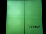
도 3 및 도 4는 본 발명의 일 실시예에 따른 실험예를 나타낸 사진이다.
111: 기판 본체 200: 봉지캔
Claims (11)
- 기판 본체;
상기 기판 본체 상에 형성된 유기 발광 소자; 그리고
상기 기판 본체와 합착되어 상기 유기 발광 소자를 밀봉 커버하는 봉지캔
을 포함하며,
상기 봉지캔은 상기 유기 발광 소자와 대향하는 면이 서로 다른 두께를 갖는 복수의 두께부들로 구분된 유기 발광 조명 장치. - 제1항에서,
상기 복수의 두께부들은 제1 두께부와, 상기 제1 두께부보다 얇은 두께를 갖는 제2 두께부를 포함하는 유기 발광 조명 장치. - 제2항에서,
상기 제2 두께부는 상기 제1 두께부보다 상기 유기 발광 소자와 상대적으로 멀리 이격된 유기 발광 조명 장치. - 제2항에서,
상기 제2 두께부와 대응하는 상기 유기 발광 소자가 상기 제1 두께부와 대응하는 상기 유기 발광 소자보다 상대적으로 높은 휘도의 빛을 방출하는 유기 발광 조명 장치. - 제2항에서,
상기 제1 두께부의 두께와 상기 제2 두께부의 두께 간의 차이는 100㎛ 보다 크거나 같은 유기 발광 조명 장치. - 제5항에서,
상기 제1 두께부는 300㎛ 내지 600㎛ 범위 내의 두께를 가지며,
상기 제2 두께부는 200㎛ 내지 500㎛ 범위 내의 두께를 갖는 유기 발광 조명 장치. - 제6항에서,
상기 봉지캔의 전체 두께는 400㎛ 내지 900㎛ 범위 내의 두께를 갖는 유기 발광 조명 장치. - 제1항에서,
상기 봉지캔의 제2 두께부는 상기 유기 발광 소자와 대향하는 면의 일부가 함몰 형성된 유기 발광 조명 장치. - 제1항 내지 제8항 중 어느 한 항에서,
상기 봉지캔은 금속 소재로 형성된 메탈캔(metal can) 및 글라스 소재로 만들어진 글라스캔(glass can) 중 하나인 유기 발광 조명 장치. - 제9항에서,
상기 제2 두께부는 숫자, 문자, 및 기호 중 하나 이상을 포함하는 도형으로 형성된 유기 발광 조명 장치. - 제10항에서,
상기 유기 발광 소자가 방출하는 빛의 휘도는 1000nit 보다 크거나 같은 유기 발광 조명 장치.
Priority Applications (3)
| Application Number | Priority Date | Filing Date | Title |
|---|---|---|---|
| KR1020110060883A KR20130008100A (ko) | 2011-06-22 | 2011-06-22 | 유기 발광 조명 장치 |
| US13/452,539 US20120326204A1 (en) | 2011-06-22 | 2012-04-20 | Organic light emitting diode lighting apparatus |
| DE102012210381A DE102012210381A1 (de) | 2011-06-22 | 2012-06-20 | Organische Licht emmitierende Dioden Beleuchtungsvorrichtung |
Applications Claiming Priority (1)
| Application Number | Priority Date | Filing Date | Title |
|---|---|---|---|
| KR1020110060883A KR20130008100A (ko) | 2011-06-22 | 2011-06-22 | 유기 발광 조명 장치 |
Publications (1)
| Publication Number | Publication Date |
|---|---|
| KR20130008100A true KR20130008100A (ko) | 2013-01-22 |
Family
ID=47321540
Family Applications (1)
| Application Number | Title | Priority Date | Filing Date |
|---|---|---|---|
| KR1020110060883A Ceased KR20130008100A (ko) | 2011-06-22 | 2011-06-22 | 유기 발광 조명 장치 |
Country Status (3)
| Country | Link |
|---|---|
| US (1) | US20120326204A1 (ko) |
| KR (1) | KR20130008100A (ko) |
| DE (1) | DE102012210381A1 (ko) |
Cited By (2)
| Publication number | Priority date | Publication date | Assignee | Title |
|---|---|---|---|---|
| KR20170001576U (ko) | 2015-10-27 | 2017-05-10 | 동우 화인켐 주식회사 | 백플레인 및 이를 포함하는 유기발광소자 |
| KR20170001578U (ko) | 2015-10-27 | 2017-05-10 | 동우 화인켐 주식회사 | 백플레인 및 이를 포함하는 유기발광소자 |
Family Cites Families (12)
| Publication number | Priority date | Publication date | Assignee | Title |
|---|---|---|---|---|
| AU5871500A (en) * | 1999-06-11 | 2001-01-02 | Sydney Hyman | Image making medium |
| WO2002021557A1 (en) * | 2000-09-06 | 2002-03-14 | Osram Opto Semiconductors Gmbh | Encapsulation for oled devices |
| KR100954016B1 (ko) * | 2002-01-23 | 2010-04-20 | 소니 주식회사 | 화상 표시 소자 및 화상 프로젝터 장치 |
| JP2004241695A (ja) * | 2003-02-07 | 2004-08-26 | Seiko Epson Corp | 光デバイスの製造方法 |
| US20040189195A1 (en) * | 2003-03-24 | 2004-09-30 | Osram Opto Semiconductors Gmbh | Devices including, methods using, and compositions of reflowable getters |
| JP4511440B2 (ja) * | 2004-10-05 | 2010-07-28 | 三星モバイルディスプレイ株式會社 | 有機発光素子及び有機発光素子の製造方法 |
| KR100670328B1 (ko) * | 2005-03-30 | 2007-01-16 | 삼성에스디아이 주식회사 | 유기 발광 표시 소자 및 그 제조방법 |
| US20070013293A1 (en) * | 2005-07-12 | 2007-01-18 | Eastman Kodak Company | OLED device having spacers |
| US7582508B2 (en) * | 2006-05-31 | 2009-09-01 | Byoung-Choo Park | Method for manufacturing an organic semiconductor device that utilizes ionic salt |
| KR101107158B1 (ko) * | 2009-07-10 | 2012-01-25 | 삼성모바일디스플레이주식회사 | 유기 발광 표시 장치 및 그 제조 방법 |
| KR101097344B1 (ko) * | 2010-03-09 | 2011-12-23 | 삼성모바일디스플레이주식회사 | 플렉서블 디스플레이 장치의 제조 방법 |
| JP2011257651A (ja) * | 2010-06-10 | 2011-12-22 | Canon Inc | 発光基板および該発光基板を備えた画像表示装置 |
-
2011
- 2011-06-22 KR KR1020110060883A patent/KR20130008100A/ko not_active Ceased
-
2012
- 2012-04-20 US US13/452,539 patent/US20120326204A1/en not_active Abandoned
- 2012-06-20 DE DE102012210381A patent/DE102012210381A1/de not_active Withdrawn
Cited By (2)
| Publication number | Priority date | Publication date | Assignee | Title |
|---|---|---|---|---|
| KR20170001576U (ko) | 2015-10-27 | 2017-05-10 | 동우 화인켐 주식회사 | 백플레인 및 이를 포함하는 유기발광소자 |
| KR20170001578U (ko) | 2015-10-27 | 2017-05-10 | 동우 화인켐 주식회사 | 백플레인 및 이를 포함하는 유기발광소자 |
Also Published As
| Publication number | Publication date |
|---|---|
| US20120326204A1 (en) | 2012-12-27 |
| DE102012210381A1 (de) | 2012-12-27 |
Similar Documents
| Publication | Publication Date | Title |
|---|---|---|
| KR101084246B1 (ko) | 유기 발광 조명 장치 | |
| US9356259B2 (en) | Organic light-emitting display apparatus and method of manufacturing the same | |
| JP5335909B2 (ja) | エレクトロルミネセント・ディスプレイ装置、照明装置または表示装置、並びに、その製造プロセス | |
| KR101456154B1 (ko) | 유기 발광 조명 장치 | |
| JP5480567B2 (ja) | 有機発光素子 | |
| JP2008091323A5 (ko) | ||
| TW200714608A (en) | Transition metal complex compound and organic electroluminescent device using the same | |
| KR20150110424A (ko) | 봉지용 적층체, 유기발광장치 및 이들의 제조방법 | |
| CN109244253B (zh) | 使用有机发光二极管的照明设备 | |
| US20130140982A1 (en) | Organic light emitting display device and manufacturing method thereof | |
| KR20130004829A (ko) | 유기 발광 조명 장치 | |
| KR20120118335A (ko) | 유기 발광 조명 장치 | |
| TWI591870B (zh) | 有機發光二極體顯示裝置 | |
| JP2011165497A (ja) | 発光装置 | |
| CN102270750A (zh) | 有机电致发光器件、显示设备及制备方法 | |
| KR20110057673A (ko) | 유기 발광 조명 장치 | |
| JP2020120113A5 (ko) | ||
| KR20130008100A (ko) | 유기 발광 조명 장치 | |
| KR101049800B1 (ko) | 유기 발광 조명 장치 | |
| JP2007531297A5 (ko) | ||
| JP5452266B2 (ja) | 発光装置 | |
| TWI327042B (en) | Double-sided organic electro-luminescence device and electronic device | |
| KR20110018234A (ko) | 유기전계발광소자 | |
| KR20110038513A (ko) | 유기 발광 표시 장치 및 그 제조 방법 | |
| KR20080068201A (ko) | 유기 발광 표시 장치 및 이의 막 두께 측정 방법 |
Legal Events
| Date | Code | Title | Description |
|---|---|---|---|
| PA0109 | Patent application |
St.27 status event code: A-0-1-A10-A12-nap-PA0109 |
|
| N231 | Notification of change of applicant | ||
| PN2301 | Change of applicant |
St.27 status event code: A-3-3-R10-R13-asn-PN2301 St.27 status event code: A-3-3-R10-R11-asn-PN2301 |
|
| P11-X000 | Amendment of application requested |
St.27 status event code: A-2-2-P10-P11-nap-X000 |
|
| P13-X000 | Application amended |
St.27 status event code: A-2-2-P10-P13-nap-X000 |
|
| PG1501 | Laying open of application |
St.27 status event code: A-1-1-Q10-Q12-nap-PG1501 |
|
| R18-X000 | Changes to party contact information recorded |
St.27 status event code: A-3-3-R10-R18-oth-X000 |
|
| A201 | Request for examination | ||
| PA0201 | Request for examination |
St.27 status event code: A-1-2-D10-D11-exm-PA0201 |
|
| D13-X000 | Search requested |
St.27 status event code: A-1-2-D10-D13-srh-X000 |
|
| D14-X000 | Search report completed |
St.27 status event code: A-1-2-D10-D14-srh-X000 |
|
| E902 | Notification of reason for refusal | ||
| PE0902 | Notice of grounds for rejection |
St.27 status event code: A-1-2-D10-D21-exm-PE0902 |
|
| E601 | Decision to refuse application | ||
| PE0601 | Decision on rejection of patent |
St.27 status event code: N-2-6-B10-B15-exm-PE0601 |
|
| R18-X000 | Changes to party contact information recorded |
St.27 status event code: A-3-3-R10-R18-oth-X000 |
|
| P22-X000 | Classification modified |
St.27 status event code: A-2-2-P10-P22-nap-X000 |
|
| P22-X000 | Classification modified |
St.27 status event code: A-2-2-P10-P22-nap-X000 |
|
| P22-X000 | Classification modified |
St.27 status event code: A-2-2-P10-P22-nap-X000 |
|
| P22-X000 | Classification modified |
St.27 status event code: A-2-2-P10-P22-nap-X000 |