KR20130015744A - Heat release printed circuit board, semiconductor illumination apparatus and display apparatus - Google Patents
Heat release printed circuit board, semiconductor illumination apparatus and display apparatus Download PDFInfo
- Publication number
- KR20130015744A KR20130015744A KR1020110077920A KR20110077920A KR20130015744A KR 20130015744 A KR20130015744 A KR 20130015744A KR 1020110077920 A KR1020110077920 A KR 1020110077920A KR 20110077920 A KR20110077920 A KR 20110077920A KR 20130015744 A KR20130015744 A KR 20130015744A
- Authority
- KR
- South Korea
- Prior art keywords
- printed circuit
- circuit board
- heat dissipation
- protrusion
- layer
- Prior art date
- Legal status (The legal status is an assumption and is not a legal conclusion. Google has not performed a legal analysis and makes no representation as to the accuracy of the status listed.)
- Withdrawn
Links
Images


Classifications
-
- H—ELECTRICITY
- H10—SEMICONDUCTOR DEVICES; ELECTRIC SOLID-STATE DEVICES NOT OTHERWISE PROVIDED FOR
- H10H—INORGANIC LIGHT-EMITTING SEMICONDUCTOR DEVICES HAVING POTENTIAL BARRIERS
- H10H20/00—Individual inorganic light-emitting semiconductor devices having potential barriers, e.g. light-emitting diodes [LED]
- H10H20/80—Constructional details
- H10H20/85—Packages
- H10H20/858—Means for heat extraction or cooling
-
- H—ELECTRICITY
- H05—ELECTRIC TECHNIQUES NOT OTHERWISE PROVIDED FOR
- H05K—PRINTED CIRCUITS; CASINGS OR CONSTRUCTIONAL DETAILS OF ELECTRIC APPARATUS; MANUFACTURE OF ASSEMBLAGES OF ELECTRICAL COMPONENTS
- H05K2201/00—Indexing scheme relating to printed circuits covered by H05K1/00
- H05K2201/10—Details of components or other objects attached to or integrated in a printed circuit board
- H05K2201/10007—Types of components
- H05K2201/10106—Light emitting diode [LED]
Landscapes
- Arrangement Of Elements, Cooling, Sealing, Or The Like Of Lighting Devices (AREA)
- Led Device Packages (AREA)
Abstract
본 발명의 일 측면에 따른 방열 인쇄회로기판은, 열전도 물질로 이루어지고, 기저부와, 발열체가 그 상단에 탑재되며 상기 기저부로부터 돌출되는 돌출부를 포함하는 방열 베이스 기판과; 절연층과, 상기 절연층 위에 적층된 회로층과, 상기 절연층 및 회로층을 관통하는 개구를 구비한 인쇄회로기판을 포함하고, 상기 인쇄회로기판은 상기 돌출부가 상기 개구에 삽입되도록 상기 방열 베이스 기판 위에 적층된다.According to an aspect of the present invention, there is provided a heat dissipation printed circuit board including a heat dissipation base substrate including a base and a heat generator mounted on an upper end thereof, and including a protrusion protruding from the base; And a printed circuit board having an insulating layer, a circuit layer stacked on the insulating layer, and an opening penetrating the insulating layer and the circuit layer, wherein the printed circuit board includes the heat dissipation base such that the protrusion is inserted into the opening. Stacked on the substrate.
Description
본 발명은 인쇄회로기판에 관한 것으로서, 특히 발열체(예를 들어, LED, LD와 같은 반도체 광원)에 의해 발생하는 열을 확산하기 위한 방열 베이스 기판을 포함하는 방열 인쇄회로기판과, 이를 구비하는 반도체 조명 장치 및 디스플레이 장치에 관한 것이다.BACKGROUND OF THE INVENTION 1. Field of the Invention The present invention relates to a printed circuit board, and more particularly, to a heat dissipation printed circuit board including a heat dissipation base substrate for diffusing heat generated by a heating element (for example, a semiconductor light source such as an LED or an LD), and a semiconductor having the same. It relates to a lighting device and a display device.
통상의 디스플레이 장치(예를 들어, TV, 휴대폰과 같은 휴대 장치, 기타 조명 장치 등)는 액정표시장치(Liquid Crystal Display: LCD), 유기발광다이오드(Organic Light Emitting Diodes: OLED) 장치 등을 포함한다.Conventional display devices (e.g., TVs, portable devices such as mobile phones, other lighting devices, etc.) include liquid crystal displays (LCDs), organic light emitting diodes (OLED) devices, and the like. .
액정표시장치는 액정층(liquid crystal layer)을 구비하고 영상을 표시하는 액정 표시 패널과, 상기 액정 표시 패널에 광을 제공하는 백라이트 유닛(back light unit: BLU)을 포함한다. 상기 액정 표시 패널은 상기 액정층과, 액정 분자들의 배열 상태를 제어하기 위해 상기 액정층의 상하에 배치된 상부 및 하부 유리 기판(upper and lower glass substrates)을 포함한다. 상기 하부 유리 기판은 박막 트랜지스터들과 화소 전극들(piexel electrodes)을 포함하고, 상기 상부 유리 기판은 공통 전극(common electrode)을 포함한다. 상기 액정 표시 패널은 상기 액정층의 상하에 배치되며 각각 입력된 광을 선편광(linear polarization)시키는 상부 및 하부 편광판(upper and lower polarization plates)을 더 포함한다. 이때, 상기 상부 및 하부 편광판의 편광 방향들은 서로 직교한다.The liquid crystal display includes a liquid crystal display panel including a liquid crystal layer and displaying an image, and a back light unit (BLU) for providing light to the liquid crystal display panel. The liquid crystal display panel includes the liquid crystal layer and upper and lower glass substrates disposed above and below the liquid crystal layer to control the arrangement of liquid crystal molecules. The lower glass substrate includes thin film transistors and pixel electrodes, and the upper glass substrate includes a common electrode. The liquid crystal display panel further includes upper and lower polarization plates disposed above and below the liquid crystal layer and linearly polarize the input light. In this case, polarization directions of the upper and lower polarizers are perpendicular to each other.
백라이트 유닛에 사용되는 광원은 형광램프, LED 램프 등이 있다. 형광램프로는 특히 냉음극 형광램프(CCFL: Cole Cathode Flourscent Lamp)가 백라이트 유닛의 광원으로 대표적이었으며, 최근에는 색 재현성, 광효율, 고수명, 저전력소모, 경량, 박형화 등의 장점을 갖는 LED 램프가 백라이트 유닛의 광원으로 채용되고 있다. 그러나 백라이트 유닛의 LED 램프는 형광램프보다 높은 온도가 발생한다는 큰 단점이 있다. LED 램프 1개당 소모 전력은 약 1W 정도이고, 1W의 소모 전력에서 열로 발생하는 비율이 70% 이상 된다. 통상 30인치 TFT-LCD의 백라이트 유닛에 사용되는 LED 램프의 수는 약 200개에 달하며, 이로 인해 발생되는 열은 약 140W 정도가 된다. 여기서 발생한 열은 백라이트 유닛 내부의 온도를 상승시켜, 백라이트 유닛을 구성하는 각종 부품들에게 영향을 주게 된다. 이로 인해 제품의 변형을 초래할 수도 있고, 열의 상승기류로 인해 백라이트 유닛의 상하 온도 차가 발생하여 응력을 초래할 수도 있으며, 이러한 문제로 인해 결국 백라이트 기능을 상실한 지경에 이르게 될 수도 있다.Light sources used in the backlight unit include fluorescent lamps, LED lamps and the like. Cold Cathode Fluorescent Lamp (CCFL: Cole Cathode Flourscent Lamp) is a typical light source for the backlight unit.In recent years, LED lamps have advantages such as color reproducibility, light efficiency, long life, low power consumption, light weight, and thinning. It is adopted as a light source of the backlight unit. However, the LED lamp of the backlight unit has a big disadvantage that a higher temperature than the fluorescent lamp. The power consumption per LED lamp is about 1W, and more than 70% of the heat generated from the 1W power consumption. Typically, the number of LED lamps used in the backlight unit of a 30-inch TFT-LCD is about 200, and the heat generated is about 140W. The heat generated here raises the temperature inside the backlight unit and affects various components of the backlight unit. This may cause deformation of the product, heat upstream of the backlight unit may cause a difference in the vertical temperature of the backlight unit may cause stress, and this problem may eventually lead to the loss of the backlight function.
전술한 바와 같은 백라이트 유닛, 일반 조명 기구 등에 활용되는 반도체 조명 장치는 반도체 광원에서 발생한 열을 효과적으로 처리하여 내부의 온도를 낮추고, 내부 온도 편차를 줄일 수 있는 수단을 필요로 한다.The semiconductor lighting device utilized in the backlight unit, the general lighting device as described above requires a means for effectively treating the heat generated from the semiconductor light source to lower the internal temperature and reduce the internal temperature deviation.
본 발명은 높은 절연전압 특성을 보유하고, 제조비가 낮으면서도, 방열 특성이 향상된 방열 인쇄회로기판과, 이를 구비한 반도체 조명 장치 및 디스플레이 장치를 제공한다. The present invention provides a heat dissipation printed circuit board having high insulation voltage characteristics and a low manufacturing cost and having improved heat dissipation characteristics, and a semiconductor lighting apparatus and a display apparatus having the same.
본 발명의 일 측면에 따른 방열 인쇄회로기판은, 열전도 물질로 이루어지고, 기저부와, 발열체가 그 상단에 탑재되며 상기 기저부로부터 돌출되는 돌출부를 포함하는 방열 베이스 기판과; 절연층과, 상기 절연층 위에 적층된 회로층과, 상기 절연층 및 회로층을 관통하는 개구를 구비한 인쇄회로기판을 포함하고, 상기 인쇄회로기판은 상기 돌출부가 상기 개구에 삽입되도록 상기 방열 베이스 기판 위에 적층된다.According to an aspect of the present invention, there is provided a heat dissipation printed circuit board including a heat dissipation base substrate including a base and a heat generator mounted on an upper end thereof, and including a protrusion protruding from the base; And a printed circuit board having an insulating layer, a circuit layer stacked on the insulating layer, and an opening penetrating the insulating layer and the circuit layer, wherein the printed circuit board includes the heat dissipation base such that the protrusion is inserted into the opening. Stacked on the substrate.
본 발명의 다른 측면에 따른 반도체 조명 장치는, 열전도 물질로 이루어지고, 기저부와, 발열체가 그 상단에 탑재되며 상기 기저부로부터 돌출되는 돌출부를 포함하는 방열 베이스 기판과; 절연층과, 상기 절연층 위에 적층된 회로층과, 상기 절연층 및 회로층을 관통하는 개구를 구비한 인쇄회로기판과; 상기 돌출부 위에 탑재되며, 상기 회로층과 전기적으로 연결되는 반도체 광원을 포함하고, 상기 인쇄회로기판은 상기 돌출부가 상기 개구에 삽입되도록 상기 방열 베이스 기판 위에 적층된다.According to another aspect of the present invention, there is provided a semiconductor lighting apparatus comprising: a heat dissipation base substrate comprising a heat conductive material, a base portion, and a heating element mounted on an upper end thereof, and including a protrusion protruding from the base portion; A printed circuit board having an insulating layer, a circuit layer laminated on the insulating layer, and an opening penetrating through the insulating layer and the circuit layer; And a semiconductor light source mounted on the protrusion and electrically connected to the circuit layer, wherein the printed circuit board is stacked on the heat dissipation base substrate such that the protrusion is inserted into the opening.
본 발명의 또 다른 측면에 따른 디스플레이 장치는 전술한 반도체 조명 장치를 포함한다. A display device according to another aspect of the present invention includes the above-described semiconductor lighting device.
본 발명에 따르면, 발생한 열을 효과적으로 처리하여 내부의 온도를 낮추고, 내부 온도 편차를 줄일 수 있으며, 높은 절연전압 특성을 보유하고, 제조비가 낮으면서도, 방열 특성이 향상된 방열 인쇄회로기판과, 이를 구비한 반도체 조명 장치 및 디스플레이 장치가 제공된다.According to the present invention, by effectively treating the generated heat to lower the internal temperature, reduce the internal temperature deviation, and has a high insulation voltage characteristics, low manufacturing cost, heat dissipation printed circuit board with improved heat dissipation characteristics, and One semiconductor lighting device and display device are provided.
즉, 본 발명에 따른 방열 인쇄회로기판에서, 발열체가 인쇄회로기판을 통하지 않고 방열 베이스 기판 위에 직접 적층되므로, 효율적이면서도 빠른 열 방출이 가능하다. 또한, 본 발명은 방열 베이스 기판을 기저부 및 돌출부로 구성하고, 발열체가 탑재되는 위치에서만 돌출부를 배치함으로써, 방열 베이스 기판의 평균적인 두께를 낮출 수 있고, 이로 인해 방열 베이스 기판의 제조 비용을 낮추면서도 방열 특성은 오히려 향상시키는 이점을 갖는다. That is, in the heat dissipation printed circuit board according to the present invention, since the heating element is directly laminated on the heat dissipation base substrate without passing through the printed circuit board, efficient and rapid heat dissipation is possible. In addition, the present invention comprises a base portion and a protrusion portion of the heat dissipation base substrate, and by arranging the protrusions only at the position where the heating element is mounted, it is possible to lower the average thickness of the heat dissipation base substrate, thereby lowering the manufacturing cost of the heat dissipation base substrate The heat dissipation characteristic has an advantage of improving rather.
도 1은 본 발명의 바람직한 제1 실시 예에 따른 반도체 조명 장치를 나타내는 도면,
도 2는 도 1에 도시된 반도체 조명 장치의 제조 방법을 설명하기 위한 흐름도,
도 3은 본 발명의 바람직한 제2 실시 예에 따른 반도체 조명 장치를 나타내는 도면,
도 4는 도 3에 도시된 반도체 조명 장치의 제조 방법을 설명하기 위한 흐름도,
도 5는 본 발명의 바람직한 제3 실시 예에 따른 반도체 조명 장치를 나타내는 도면,
도 6은 도 5에 도시된 반도체 조명 장치의 제조 방법을 설명하기 위한 흐름도.1 is a view showing a semiconductor lighting apparatus according to a first embodiment of the present invention,
2 is a flowchart illustrating a method of manufacturing the semiconductor lighting apparatus shown in FIG. 1;
3 is a view showing a semiconductor lighting apparatus according to a second embodiment of the present invention;
4 is a flowchart for describing a method of manufacturing the semiconductor lighting apparatus shown in FIG. 3;
5 is a view showing a semiconductor lighting apparatus according to a third embodiment of the present invention;
FIG. 6 is a flowchart for explaining a method of manufacturing the semiconductor lighting apparatus shown in FIG. 5. FIG.
이하 본 발명의 바람직한 실시 예들을 첨부한 도면을 참조하여 상세히 설명한다. 하기 설명에서는 구체적인 구성 소자 등과 같은 특정 사항들이 나타나고 있는데 이는 본 발명의 보다 전반적인 이해를 돕기 위해서 제공된 것일 뿐 이러한 특정 사항들이 본 발명의 범위 내에서 소정의 변형이나 혹은 변경이 이루어질 수 있음은 이 기술분야에서 통상의 지식을 가진 자에게는 자명하다 할 것이다. 또한, 본 발명을 설명함에 있어서 본 발명과 관련된 공지 기술에 대한 구체적인 설명이 본 발명의 요지를 불필요하게 흐릴 수 있다고 판단되는 경우에 그 상세한 설명을 생략하기로 한다.Hereinafter, preferred embodiments of the present invention will be described in detail with reference to the accompanying drawings. In the following description, specific matters such as specific elements are shown, which are provided to help a more general understanding of the present invention. It is self-evident to those of ordinary knowledge in Esau. In the following description, well-known functions or constructions are not described in detail since they would obscure the invention in unnecessary detail.
이하의 실시 예들에서는, 발열체의 대표적인 예로서 반도체 광원을 들고 있으나, 본 발명의 방열 인쇄회로기판은 이러한 반도체 광원에만 적용되는 것이 아니라, 마이크로 프로세서, 구동 모듈, 통신 모듈, 반도체 광원 등과 같은 열이 발생하는 임의의 전자 모듈(또는 반도체 칩)에 적용될 수 있음에 주의하여야 한다. In the following embodiments, a semiconductor light source is used as a representative example of a heating element, but the heat dissipation printed circuit board of the present invention is not applied only to the semiconductor light source, but heat such as a microprocessor, a driving module, a communication module, and a semiconductor light source is generated. It should be noted that the present invention can be applied to any electronic module (or semiconductor chip).
또한, 방열 인쇄회로기판의 대표적인 적용 예로서 반도체 조명 장치를 들고 있으나, 본 발명이 이에 한정되지 않음은 당업자에게 자명할 것이다. In addition, although a semiconductor lighting device is a typical application example of a heat dissipation printed circuit board, it will be apparent to those skilled in the art that the present invention is not limited thereto.
도 1은 본 발명의 바람직한 제1 실시 예에 따른 반도체 조명 장치를 나타내는 도면이다. 상기 반도체 조명 장치(100)는 방열 베이스 기판(110) 및 인쇄회로기판(120)을 구비한 방열 인쇄회로기판(105)과, 반사 부재(130)와, 반도체 광원(140)을 포함한다. 1 is a view showing a semiconductor lighting apparatus according to a first embodiment of the present invention. The
상기 방열 베이스 기판(110)은 열전도 물질로 이루어지고, 기저부(112)와, 상기 기저부(112)로부터 상향으로 돌출된 적어도 하나의 돌출부(114)를 포함한다. 상기 열전도 물질로는 알루미늄, 구리 등과 같은 방열 성능을 가지는 금속 물질 등을 사용할 수 있고, 바람직하게는 그래파이트 물질 또는 그래파이트 함유 물질을 사용할 수 있다. 그래파이트 물질은, 예를 들어, 첨가물을 전혀 사용하지 않은 정제된 천연 인상흑연을 산처리 및 고온처리하여 가공된 순수흑연 물질이고, 내열성, 내약품성 등 흑연만의 독특한 특성을 지녀 유연성(flexible) 및 압축 복원력이 뛰어나다. 또한, 그래파이트 물질은 카본이 층 구조를 이룬 것으로, 각 층 면 방향의 분자는 공유결합에 의해 강고하게 결합하여 면 방향으로 열을 잘 확산시키는 이방성 특성을 갖는다. 바람직하게는, 상기 방열 베이스 기판은 그래파이트 시트를 포함하거나, 그래파이트 성형체일 수 있다. 예를 들어, 상기 방열 베이스 기판은 Al, Ni, Cu 등의 열전도성이 높은 금속 파우더, 또는 그래파이트 파우더, 또는 이들의 혼합물을 성형(압축 또는 압출)하여 제조될 수 있다. 이러한 파우더 성형은 기계 가공에 비하여 제조가 용이하고, 제조 비용이 저렴하다는 이점을 갖는다. The heat dissipation base substrate 110 is made of a thermally conductive material, and includes a
상기 방열 베이스 기판(110)의 기저부(112)는 임의의 형태를 가질 수 있고, 예를 들어 사각 판, 원형 판, 타원 판 등의 형태를 가질 수 있다. 바람직하게는, 상기 기저부(112)의 상면 및 하면은 각각 전체 면적에 걸쳐서 평면이고, 전체적으로 균일한 두께를 갖는다. The
상기 돌출부(114)는 상기 기저부(112)의 상단으로부터 기설정된 높이로 상향 돌출되며, 상기 돌출부(114)는 임의의 형태를 가질 수 있고, 예를 들어 사각 기둥, 원기둥, 타원 기둥 등의 형태를 가질 수 있다. 바람직하게는, 상기 돌출부(114)의 상면은 전체 면적에 걸쳐서 평면이고, 전체적으로 균일한 두께를 갖는다. 도 1에는 하나의 돌출부(114)만이 예시되어 있으나, 상기 방열 베이스 기판(110)은 행렬 구조(예를 들어, 5행 5열)로 배치된 다수의 돌출부들을 구비할 수 있다. 바람직하게는, 상기 돌출부(114)의 두께는 상기 기저부(112)의 두께의 0.3~1배의 범위 내에 있으며, 상기 인쇄회로기판(120)의 두께보다 작거나 같다. 또한, 상기 반도체 광원(140)이 상기 돌출부(114)의 상면 위에 탑재되기 때문에, 상기 돌출부(114)의 표면적은 상기 반도체 광원(140)의 표면적보다 크다. The
상기 기저부(112) 및 돌출부(114)는 동일한 물질로 일체 형성되거나, 서로 다른 재질로 형성된 후, 부착(접착, 융착 등)될 수도 있다. The
상기 인쇄회로기판(120)은 전기적 절연층(122)과, 상기 절연층(122) 위에 적층된 도전성 회로층(124)과, 상기 절연층(122) 및 회로층(124)을 관통하는 적어도 하나의 개구(126)를 구비한다. 상기 회로층(124)은 상기 반도체 광원(140)에 바이어스 전압을 포함하는 구동 신호를 인가하기 위한(즉, 상기 반도체 광원(140)을 구동하기 위한) 기설정된 패턴을 갖는다. 상기 돌출부(114)가 상기 개구(126)에 삽입될 수 있도록, 상기 돌출부(114)의 표면적은 상기 개구(126)의 표면적보다 작거나 같다. 상기 인쇄회로기판(120)은 상기 돌출부(114)가 상기 개구(126)에 삽입되도록 상기 기저부(112) 위에 적층된다. 상기 절연층(122)은 상기 인쇄회로기판(120)의 원판에 해당하며, 바람직하게는 FR4(FR=Frame Retadent), 즉 유리/에폭시 복합재로 이루어질 수 있다. The printed
상기 반사 부재(130)는 하나의 층이거나 표면일 수 있으며, 상기 반도체 광원(140)으로부터 입사된 광을 되반사함으로써, 상기 반도체 광원(140)의 발광 효율을 향상시킨다. 상기 반사 부재(130)는 상기 돌출부(114)의 상면에 반사율(예를 들어, 90% 이상)이 높은 Al, Ag, Cr 등의 금속 물질을 적층(증착, 인쇄 등)함으로써 형성되거나, 상기 돌출부(114)의 상면을 폴리싱함으로써 형성될 수 있다. The
상기 반사 부재(130)의 표면이 평면인 경우에, 상기 반사 부재(130)로부터 반사된 광은 발산할 수 있으며, 이러한 경우에 발산된 광이 조명에 기여하는 정도가 작을 수 있다. 따라서, 상기 돌출부(114)의 상면을 오목한 곡면으로 형성함으로써, 상기 반사 부재(130)로부터 반사된 광이 수렴하거나 시준화되도록 할 수도 있다. 예를 들어, 상기 돌출부(114)의 상면은 적어도 그 중심부에서 기설정된 곡률을 가질 수 있으며, 상기 돌출부(114)의 상면의 적어도 중심부는 구면 또는 비구면(타원면 등)일 수 있다. When the surface of the
상기 반도체 광원(140)은 상기 반사 부재(130)의 상면 위에 탑재되며, 와이어(150) 본딩을 통해 상기 회로층(124)과 전기적으로 연결된다. 상기 반도체 광원(140)은, LED, LD 등과 같이, 복수의 반도체 층들을 적층하여 형성되고, 전류 주입에 따라 광을 방출한다. The
도 2는 도 1에 도시된 반도체 조명 장치의 제조 방법을 설명하기 위한 흐름도이다. 상기 제조 방법은 방열 베이스 기판 제공 단계(S110)와, 반사 부재 형성 단계(S120)와, 인쇄회로기판 제공 단계(S130)와, 기판 부착 단계(S140)와, 광원 탑재 단계(S150)를 포함한다. FIG. 2 is a flowchart for explaining a method of manufacturing the semiconductor lighting apparatus shown in FIG. 1. The manufacturing method includes a heat radiation base substrate providing step S110, a reflective member forming step S120, a printed circuit board providing step S130, a substrate attaching step S140, and a light source mounting step S150. .
상기 방열 베이스 기판 제공 단계(S110)에서, 열전도 물질로 이루어지고, 기저부(112)와, 상기 기저부(112)로부터 상향으로 돌출된 적어도 하나의 돌출부(114)를 포함하는 방열 베이스 기판(110)을 준비한다. 예를 들어, 그래파이트 파우더와 에폭시 파우더를 기설정된 비율로 혼합하고, 혼합물을 프레스 성형하여 상기 방열 베이스 기판(110)을 형성한다. 예를 들어, 그래파이트 파우더 90wt% 및 에폭시 파우더 10wt%의 비율로 혼합될 수 있다. 본 예와 다르게, 금속 재질의 판을 성형(절삭, 부식 등)함으로써, 상기 방열 베이스 기판(110)을 형성할 수도 있다. 예를 들어, 알루미늄 재질의 판을 부식함으로써, 상기 방열 베이스 기판(110)을 형성한다. In the providing of the heat dissipation base substrate (S110), the heat dissipation base substrate 110 includes a
상기 반사 부재 형성 단계(S120)에서, 상기 돌출부(114)의 상면에 반사 부재(130)를 적층한다. 예를 들어, 상기 돌출부(114)의 상면에 Ni, Cr, Ag, Cu, 또는 다른 금속 물질을 코팅하여 상기 반사 부재(130)를 형성한다. In the reflective member forming step (S120), the
상기 인쇄회로기판 제공 단계(S130)에서, 전기적 절연층(122)과, 상기 절연층(122) 위에 적층된 도전성 회로층(124)과, 상기 절연층(122) 및 회로층(124)을 관통하는 적어도 하나의 개구를 구비하는 인쇄회로기판(120)을 준비한다. 예를 들어, 상기 인쇄회로기판(120)은 FR4 원판의 기설정된 위치들에 적어도 하나의 개구(126)를 형성하고, 상기 가공된 FR4 원판의 상면에 기설정된 도전성 회로층을 적층함으로써 형성될 수 있다. 예를 들어, 상기 인쇄회로기판(120)은 0.4t(=0.4mm)의 두께를 가질 수 있다. In the providing of the printed circuit board (S130), the electrical insulating
상기 기판 부착 단계(S140)에서, 상기 인쇄회로기판(120)과 상기 기저부(112)의 사이에 본딩 시트, 프리프레그(prepreg) 등과 같은 접착 부재를 위치시키고, 상기 돌출부(114)가 상기 인쇄회로기판(120)의 개구(126)에 삽입되도록, 상기 기저부(112) 위에 상기 인쇄회로기판(120)을 탑재한다. 이후, 핫 프레스(hot press) 장치를 이용하여 상기 인쇄회로기판(120) 및 기저부(112)를 열간 압착한다. 예를 들어, 상기 프리프레그는 60㎛의 두께를 가질 수 있다. 바람직하게는, 상기 인쇄회로기판(120)의 하면은 기저부(112)의 상면에 부착되고, 상기 개구(126)의 벽을 이루는 상기 인쇄회로기판(120)의 내측면은 상기 돌출부(114)의 외측면과 부착 또는 밀착된다.In the substrate attaching step (S140), an adhesive member such as a bonding sheet, a prepreg, or the like is disposed between the printed
상기 반도체 광원 탑재 단계(S150)에서, 상기 반사 부재(130)의 상면에 반도체 광원(140)을 탑재하고, 상기 반도체 광원(140)과 상기 회로층(124)을 와이어(150) 본딩을 통해 전기적으로 연결한다. 상기 반도체 광원(140)의 상면 중앙부에는 광을 외부로 출사하는 발광 영역이 존재하고, 상기 발광 영역의 주위에 와이어 본딩을 위한 본딩 패드들을 배치되고, 상기 본딩 패드들 및 상기 회로층(124)이 와이어(150) 본딩을 통해 서로 연결된다. In the semiconductor light source mounting step (S150), the
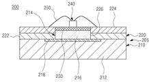
도 3은 본 발명의 바람직한 제2 실시 예에 따른 반도체 조명 장치를 나타내는 도면이다. 상기 반도체 조명 장치(200)는 방열 베이스 기판(210) 및 인쇄회로기판(220)을 구비한 방열 인쇄회로기판(205)과, 반사 부재(230)와, 반도체 광원(240)을 포함한다. 상기 반도체 조명 장치(200)는 도 1에 도시된 반도체 조명 장치(100)와 비교하여, 돌출부(214)에 있어서만 큰 차이가 있으므로, 중복되는 설명은 생략하기로 하나, 동일한 용어의 소자에 대해 도 1에 관한 설명을 준용할 수 있음은 자명하다. 3 is a view showing a semiconductor lighting apparatus according to a second embodiment of the present invention. The
상기 방열 베이스 기판(210)은 열전도 물질로 이루어지고, 기저부(212)와, 상기 기저부(212)로부터 상향으로 돌출된 적어도 하나의 돌출부(214)를 포함한다. 상기 돌출부(214)는 상기 기저부(212)와는 상이한 재질로 형성되며, 상기 기저부(212)의 열전도성보다 높은 열전도성을 갖는다. 예를 들어, 상기 기저부(212)는 그래파이트 물질로 이루어지고, 상기 돌출부(214)는 Al, Cu 등의 금속 물질로 이루어질 수 있다. The heat
상기 돌출부(214)는 상기 기저부(212)의 상단으로부터 기설정된 높이로 상향 돌출되며, 상기 돌출부(214)는 임의의 형태를 가질 수 있고, 예를 들어 사각 기둥, 원기둥, 타원 기둥 등의 형태를 가질 수 있다. 도 3에서는, 상기 돌출부(214)가 몸체부(216)와 상기 몸체부(216)의 하단에서 외측으로 연장된 플랜지(218)를 포함하는 것으로 예시되어 있다. 상기 돌출부(214)는 상기 반도체 광원(240)에 의해 발생한 열을 상기 기저부(212)로 전달하는 열전달 매개체로서 기능하며, 또한 상기 반사층(230)의 형성을 위한 반사층 베이스로서 기능한다. 상기 플랜지(218)가 상기 인쇄회로기판(220)과 상기 기저부(212)의 사이에 위치함으로써, 상기 플랜지(218)는 상기 인쇄회로기판(220) 내의 열을 상기 기저부(212)로 전달하는 기능을 한다. 바람직하게는, 상기 돌출부(214)의 상면은 전체 면적에 걸쳐서 평면이고, 상기 몸체부(216) 및 플랜지(218) 각각은 전체적으로 균일한 두께를 갖는다.The
상기 기저부(212) 및 돌출부(214)는 서로 다른 재질로 형성된 후 서로 부착(접착, 융착 등)되거나, 이중 사출 성형을 통해 형성될 수 있다. The
상기 인쇄회로기판(220)은 전기적 절연층(222)과, 상기 절연층(222) 위에 적층된 도전성 회로층(224)과, 상기 절연층(222) 및 회로층(224)을 관통하는 적어도 하나의 개구(226)를 구비한다. 상기 인쇄회로기판(220)은 상기 돌출부(214)가 상기 개구(226)에 삽입되도록 상기 기저부(212) 위에 적층된다. The printed
상기 반사 부재(230)는 상기 돌출부(214)의 상면에 반사율(예를 들어, 90% 이상)이 높은 Ni, Cr, Ag, Cu 등의 금속 물질을 적층(증착, 인쇄 등)함으로써 형성되거나, 상기 돌출부(214)의 상면을 폴리싱함으로써 형성될 수 있다. 상기 반사 부재(230)는 상기 돌출부(214)의 재질과는 다른 재질로 형성될 수 있다. The
상기 반도체 광원(240)은 상기 반사 부재(230)의 상면 위에 탑재되며, 와이어(250) 본딩을 통해 상기 회로층(224)과 전기적으로 연결된다. The
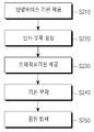
도 4는 도 3에 도시된 반도체 조명 장치의 제조 방법을 설명하기 위한 흐름도이다. 상기 제조 방법은 방열 베이스 기판 제공 단계(S210)와, 반사 부재 형성 단계(S220)와, 인쇄회로기판 제공 단계(S230)와, 기판 부착 단계(S240)와, 반도체 광원 탑재 단계(S250)를 포함한다. FIG. 4 is a flowchart for explaining a method of manufacturing the semiconductor lighting apparatus shown in FIG. 3. The manufacturing method includes a heat dissipation base substrate providing step S210, a reflective member forming step S220, a printed circuit board providing step S230, a substrate attaching step S240, and a semiconductor light source mounting step S250. do.
상기 방열 베이스 기판 제공 단계(S210)에서, 열전도 물질로 이루어지고, 기저부(212)와, 상기 기저부(212)로부터 상향으로 돌출된 적어도 하나의 돌출부(214)를 포함하는 방열 베이스 기판(210)을 준비한다. 예를 들어, 그래파이트 파우더와 에폭시 파우더를 기설정된 비율로 혼합하고, 혼합물을 프레스 성형하여 상기 기저부(212)를 형성한다. 상기 기저부(212)보다 열전도성이 높은 Al, Cu 등의 금속 재질로 사출 성형 등을 통해 상기 돌출부(214)를 형성한다. 이후, 상기 기저부(212) 및 돌출부(214)를 서로 부착한다. In the providing of the heat dissipation base substrate (S210), the heat
상기 반사 부재 형성 단계(S220)에서, 상기 돌출부(214)의 상면에 반사 부재(230)를 적층한다. 예를 들어, 상기 돌출부(214)의 상면에 Ni, Cr, Ag, Cu 또는 다른 금속 물질을 코팅하여 상기 반사 부재(230)를 형성한다. 상기 반사 부재(230)는, 상기 기저부(212) 및 돌출부(214)를 서로 부착하기 이전에, 상기 돌출부(214)의 상면에 미리 형성될 수 있다. In the forming of the reflective member (S220), the
상기 인쇄회로기판 제공 단계(S230)에서, 전기적 절연층(222)과, 상기 절연층(222) 위에 적층된 도전성 회로층(224)과, 상기 절연층(222) 및 회로층(224)을 관통하는 적어도 하나의 개구(226)를 구비하는 인쇄회로기판(220)을 준비한다. In the providing of the printed circuit board (S230), the electrical insulating
상기 기판 부착 단계(S240)에서, 상기 인쇄회로기판(220)과 상기 기저부(212)의 사이에 본딩 시트, 프리프레그(prepreg) 등과 같은 접착 부재를 위치시키고, 상기 돌출부(214)가 상기 인쇄회로기판(220)의 개구(226)에 삽입되도록, 상기 기저부(212) 위에 상기 인쇄회로기판(220)을 탑재한다. 이후, 핫 프레스 장치를 이용하여 상기 인쇄회로기판(220) 및 기저부(212)를 열간 압착한다. In the substrate attaching step (S240), an adhesive member such as a bonding sheet, a prepreg, or the like is disposed between the printed
상기 반도체 광원 탑재 단계(S250)에서, 상기 반사 부재(230)의 상면에 반도체 광원(240)을 탑재하고, 상기 반도체 광원(240)과 상기 회로층(224)을 와이어(250) 본딩을 통해 전기적으로 연결한다. In the semiconductor light source mounting step (S250), the
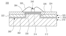
도 5는 본 발명의 바람직한 제3 실시 예에 따른 반도체 조명 장치를 나타내는 도면이다. 상기 반도체 조명 장치(300)는 방열 베이스 기판(310) 및 인쇄회로기판(320)을 구비한 방열 인쇄회로기판(305)과, 반사 부재(330)와, 반도체 광원(340)과, 열전달층(260)을 포함한다. 상기 반도체 조명 장치(300)는 도 1에 도시된 반도체 조명 장치(100)와 비교하여, 열전달층(260)을 더 포함한다는 점에 있어서만 큰 차이가 있으므로, 중복되는 설명은 생략하기로 하나, 동일한 용어의 소자에 대해 도 1에 관한 설명을 준용할 수 있음은 자명하다. 5 is a diagram illustrating a semiconductor lighting apparatus according to a third exemplary embodiment of the present invention. The
상기 방열 베이스 기판(310)은 열전도 물질로 이루어지고, 기저부(312)와, 상기 기저부(312)로부터 상향으로 돌출된 적어도 하나의 돌출부(314)를 포함한다. The heat
상기 돌출부(314)는 상기 기저부(312)의 상단으로부터 기설정된 높이로 상향 돌출되며, 상기 돌출부(314)는 임의의 형태를 가질 수 있고, 예를 들어 사각 기둥, 원기둥, 타원 기둥 등의 형태를 가질 수 있다. The
상기 인쇄회로기판(320)은 전기적 절연층(322)과, 상기 절연층(322) 위에 적층된 도전성 회로층(324)과, 상기 절연층(322) 및 회로층(324)을 관통하는 적어도 하나의 개구(326)를 구비한다. 상기 인쇄회로기판(320)은 상기 돌출부(314)가 상기 개구(326)에 삽입되도록 상기 기저부(312) 위에 적층된다. The printed
상기 열전달층(360)은 상기 방열 베이스 기판(310)의 상면 전체에 적층되며, 상기 열전달층(360)은 상기 방열 베이스 기판(310)의 열전도성보다 높은 열전도성을 갖는다. 예를 들어, 상기 방열 베이스 기판(310)은 그래파이트 물질로 이루어지고, 상기 열전달층(360)은 Al, Cu 등의 금속 물질로 이루어질 수 있다. 본 예에서, 상기 열전달층(360)은 상기 방열 베이스 기판(310)의 상면 전체에 적층되어 있으나, 상기 돌출부(314)의 외측면을 포함한 상기 방열 베이스 기판(310)의 상면 일부에만 형성될 수도 있다. 상기 열전달층(360)은 유연한 금속 시트(또는 포일(foil))로 이루어지거나, 증착 등을 통해 형성될 수 있다. 상기 열전달층(360)은 상기 방열 베이스 기판(310)의 상면의 굴곡에 따라서, 평탄부(362) 및 굴곡부(364)를 포함하며, 상기 평탄부(362)는 상기 기저부(312) 위에 적층되고, 상기 굴곡부(364)는 상기 돌출부(314) 위에 적층된다. The
상기 반사 부재(330)는 상기 굴곡부(364)의 상면에 반사율(예를 들어, 90% 이상)이 높은 Ni, Cr, Ag, Cu 등의 금속 물질을 적층(증착, 인쇄 등)함으로써 형성되거나, 상기 굴곡부(364)의 상면을 폴리싱함으로써 형성될 수 있다. 상기 반사 부재(330)는 상기 열전달층(360)의 재질과는 다른 재질로 형성될 수 있다. 상기 열전달층(360)은 상기 반도체 광원(340)에 의해 발생한 열을 상기 기저부(312)로 전달하는 열전달 매개체로서 기능하며, 또한 상기 반사층(330)의 형성을 위한 반사층 베이스로서 기능한다.The
상기 반도체 광원(340)은 상기 반사 부재(330)의 상면 위에 탑재되며, 와이어(350) 본딩을 통해 상기 회로층(324)과 전기적으로 연결된다. The
도 6은 도 5에 도시된 반도체 조명 장치의 제조 방법을 설명하기 위한 흐름도이다. 상기 제조 방법은 방열 베이스 기판 제공 단계(S310)와, 열전달층 적층 단계(S320)와, 반사 부재 형성 단계(S330)와, 인쇄회로기판 제공 단계(S340)와, 기판 부착 단계(S350)와, 광원 탑재 단계(360)를 포함한다. 6 is a flowchart for describing a method of manufacturing the semiconductor lighting apparatus illustrated in FIG. 5. The manufacturing method includes the step of providing a heat dissipation base substrate (S310), a heat transfer layer stacking step (S320), a reflective member forming step (S330), a printed circuit board providing step (S340), a substrate attaching step (S350), A light
상기 방열 베이스 기판 제공 단계(S310)에서, 열전도 물질로 이루어지고, 기저부(312)와, 상기 기저부(312)로부터 상향으로 돌출된 적어도 하나의 돌출부(314)를 포함하는 방열 베이스 기판(310)을 준비한다. In the providing of the heat dissipation base substrate (S310), the heat
상기 열전달층 적층 단계(S320)에서, 상기 열전달층(360)을 상기 방열 베이스 기판(310)의 상면에 적층한다. 상기 열전달층(360)은 상기 방열 베이스 기판(310)의 열전도성보다 높은 열전도성을 갖는다. 예를 들어, 상기 열전달층(360)은 Al, Cu 등의 금속 재질로 형성될 수 있으며, 금속 재질의 포일을 상기 방열 베이스 기판(310)의 상면에 부착한다. In the heat transfer layer stacking step (S320), the
상기 반사 부재 형성 단계(S330)에서, 상기 열전달층(360)의 굴곡부(364)의 상면에 반사 부재(330)를 적층한다. 예를 들어, 상기 굴곡부(364)의 상면에 Ni, Cr, Ag, Cu 또는 다른 금속 물질을 코팅하여 상기 반사 부재(330)를 형성한다. In the forming of the reflective member (S330), the
상기 인쇄회로기판 제공 단계(S340)에서, 전기적 절연층(322)과, 상기 절연층(322) 위에 적층된 도전성 회로층(324)과, 상기 절연층(322) 및 회로층(324)을 관통하는 적어도 하나의 개구(326)를 구비하는 인쇄회로기판(320)을 준비한다. In the providing of the printed circuit board (S340), the electrical insulating
상기 기판 부착 단계(S350)에서, 상기 인쇄회로기판(320)과 상기 열전달층(360)의 평탄부(362)의 사이에 본딩 시트, 프리프레그(prepreg) 등과 같은 접착 부재를 위치시키고, 상기 돌출부(314)가 상기 인쇄회로기판(320)의 개구(326)에 삽입되도록, 상기 평탄부(362) 위에 상기 인쇄회로기판(310)을 탑재한다. 이후, 핫 프레스 장치를 이용하여 상기 인쇄회로기판(310) 및 평탄부(362)를 열간 압착한다. In the substrate attaching step S350, an adhesive member such as a bonding sheet, a prepreg, and the like is disposed between the printed
상기 반도체 광원 탑재 단계(S360)에서, 상기 반사 부재(330)의 상면에 반도체 광원(340)을 탑재하고, 상기 반도체 광원(340)과 상기 회로층(324)을 와이어(350) 본딩을 통해 전기적으로 연결한다.In the semiconductor light source mounting step (S360), the
전술한 바와 같은 본 발명의 반도체 조명 장치는 임의의 전자 장치(또는 반도체 장치)에 적용될 수 있고, 바람직하게는 디스플레이 장치(예를 들어, 텔레비전(television: TV), 휴대폰, PDA(personal digital assistant), PMP(portable multimedia player), MP3 플레이어 등과 같은 휴대용 디스플레이 장치, 백라이트 유닛, 기타 조명 장치 등)에 포함될 수 있다. The semiconductor lighting apparatus of the present invention as described above can be applied to any electronic device (or semiconductor device), and preferably a display device (for example, a television (TV), a mobile phone, a personal digital assistant) , Portable display devices such as portable multimedia players (PMPs), MP3 players, backlight units, and other lighting devices.
100: 반도체 광원 장치, 110: 방열 베이스 기판, 120: 인쇄회로기판, 130: 반사 부재, 140: 반도체 광원, 150: 와이어100: semiconductor light source device, 110: heat dissipation base substrate, 120: printed circuit board, 130: reflective member, 140: semiconductor light source, 150: wire
Claims (11)
열전도 물질로 이루어지고, 기저부와, 발열체가 그 상단에 탑재되며 상기 기저부로부터 돌출되는 돌출부를 포함하는 방열 베이스 기판과;
절연층과, 상기 절연층 위에 적층된 회로층과, 상기 절연층 및 회로층을 관통하는 개구를 구비한 인쇄회로기판을 포함하고,
상기 인쇄회로기판은 상기 돌출부가 상기 개구에 삽입되도록 상기 방열 베이스 기판 위에 적층됨을 특징으로 하는 방열 인쇄회로기판.In heat dissipation printed circuit board,
A heat dissipation base substrate made of a thermally conductive material and including a base and a protrusion mounted on an upper portion of the heating element and protruding from the base;
A printed circuit board having an insulating layer, a circuit layer laminated on the insulating layer, and an opening penetrating through the insulating layer and the circuit layer,
And the printed circuit board is stacked on the heat dissipation base substrate such that the protrusion is inserted into the opening.
상기 방열 베이스 기판은 그래파이트를 함유한 물질로 형성됨을 특징으로 하는 방열 인쇄회로기판.The method of claim 1,
The heat dissipation base substrate is a heat dissipation printed circuit board, characterized in that formed of a material containing graphite.
상기 인쇄회로기판의 절연층은 유리/에폭시 복합재로 형성됨을 특징으로 하는 방열 인쇄회로기판.The method of claim 1,
Thermal insulation printed circuit board, characterized in that the insulating layer of the printed circuit board is formed of a glass / epoxy composite.
상기 돌출부는 상기 기저부보다 열전도성이 높은 다른 재질로 형성됨을 특징으로 하는 방열 인쇄회로기판.The method of claim 1,
And the protrusion is formed of another material having higher thermal conductivity than the base.
상기 방열 베이스 기판 및 상기 인쇄회로기판의 사이에 적층되고, 상기 방열 베이스 기판보다 높은 열전도성을 갖는 다른 재질의 열전달층을 더 포함함을 특징으로 하는 방열 인쇄회로기판.The method of claim 1,
And a heat transfer layer of another material stacked between the heat dissipation base substrate and the printed circuit board and having a higher thermal conductivity than the heat dissipation base substrate.
상기 발열체는 마이크로 프로세서, 구동 모듈, 통신 모듈 및 반도체 광원 중의 하나임을 특징으로 하는 방열 인쇄회로기판.The method of claim 1,
The heating element is a heat dissipation printed circuit board, characterized in that one of a microprocessor, a drive module, a communication module and a semiconductor light source.
상기 돌출부 위에 탑재되며, 상기 회로층과 전기적으로 연결되는 반도체 광원을 더 포함함을 특징으로 하는 반도체 조명 장치.A heat dissipation printed circuit board of any one of claims 1 to 5,
And a semiconductor light source mounted on the protrusion and electrically connected to the circuit layer.
상기 돌출부의 상면에 반사 부재가 적층되고, 상기 반도체 광원은 상기 반사 부재의 상면에 탑재됨을 특징으로 하는 반도체 조명 장치.The method of claim 7, wherein
A reflective member is stacked on an upper surface of the protrusion, and the semiconductor light source is mounted on an upper surface of the reflective member.
상기 반도체 광원은 LED(light emitting diode)인 것을 특징으로 하는 반도체 조명 장치.The method of claim 7, wherein
And the semiconductor light source is a light emitting diode (LED).
상기 디스플레이 장치는 텔레비전, 휴대폰 및 백라이트 유닛 중의 하나임을 특징으로 하는 디스플레이 장치.The method of claim 10,
And the display device is one of a television, a mobile phone and a backlight unit.
Priority Applications (1)
| Application Number | Priority Date | Filing Date | Title |
|---|---|---|---|
| KR1020110077920A KR20130015744A (en) | 2011-08-04 | 2011-08-04 | Heat release printed circuit board, semiconductor illumination apparatus and display apparatus |
Applications Claiming Priority (1)
| Application Number | Priority Date | Filing Date | Title |
|---|---|---|---|
| KR1020110077920A KR20130015744A (en) | 2011-08-04 | 2011-08-04 | Heat release printed circuit board, semiconductor illumination apparatus and display apparatus |
Publications (1)
| Publication Number | Publication Date |
|---|---|
| KR20130015744A true KR20130015744A (en) | 2013-02-14 |
Family
ID=47895493
Family Applications (1)
| Application Number | Title | Priority Date | Filing Date |
|---|---|---|---|
| KR1020110077920A Withdrawn KR20130015744A (en) | 2011-08-04 | 2011-08-04 | Heat release printed circuit board, semiconductor illumination apparatus and display apparatus |
Country Status (1)
| Country | Link |
|---|---|
| KR (1) | KR20130015744A (en) |
Cited By (3)
| Publication number | Priority date | Publication date | Assignee | Title |
|---|---|---|---|---|
| KR101321789B1 (en) * | 2013-03-14 | 2013-11-04 | 채현우 | A method for fabricating module with led lamp |
| CN107889338A (en) * | 2016-09-30 | 2018-04-06 | 雅达电子国际有限公司 | Heat sink assemblies for surface mount devices |
| KR20220138095A (en) * | 2021-04-05 | 2022-10-12 | 주식회사 테라닉스 | Printed circuit board, manufacturing method of the board and metal body for heat radiation used for the manufacturing |
-
2011
- 2011-08-04 KR KR1020110077920A patent/KR20130015744A/en not_active Withdrawn
Cited By (4)
| Publication number | Priority date | Publication date | Assignee | Title |
|---|---|---|---|---|
| KR101321789B1 (en) * | 2013-03-14 | 2013-11-04 | 채현우 | A method for fabricating module with led lamp |
| WO2014142435A1 (en) * | 2013-03-14 | 2014-09-18 | 주식회사 오알알아이에스 | Led module manufacturing method |
| CN107889338A (en) * | 2016-09-30 | 2018-04-06 | 雅达电子国际有限公司 | Heat sink assemblies for surface mount devices |
| KR20220138095A (en) * | 2021-04-05 | 2022-10-12 | 주식회사 테라닉스 | Printed circuit board, manufacturing method of the board and metal body for heat radiation used for the manufacturing |
Similar Documents
| Publication | Publication Date | Title |
|---|---|---|
| CN207123684U (en) | Flexible surface light source and its electronic equipment | |
| TWI289366B (en) | Light source unit, illumination device using the same, and display device using the same | |
| CN108732816B (en) | Area source backlight module and liquid crystal display panel | |
| US8132935B2 (en) | Light emitting module | |
| CN1983590B (en) | High brightness light emitting diode and liquid crystal display device using same | |
| KR101255833B1 (en) | Liquid crystal display device | |
| KR101774277B1 (en) | Liquid crystal display device | |
| CN105158973A (en) | Liquid crystal display device | |
| KR101303595B1 (en) | A heat radiating printed circuit board, method of manufacturing the heat radiating printed circuit board, backlight unit including the heat radiating printed circuit board and liquid crystal display including the same | |
| TW201133086A (en) | Liquid crystal display device | |
| CN101452924A (en) | Led backlight for a liquid crystal display device | |
| CN105276445A (en) | Backlight device | |
| CN106154646A (en) | A kind of lamp plate, backlight module and liquid crystal indicator | |
| KR20130048408A (en) | Heat release printed circuit board, semiconductor illumination apparatus and display apparatus | |
| KR20130015744A (en) | Heat release printed circuit board, semiconductor illumination apparatus and display apparatus | |
| CN116413956A (en) | Lamp panel, manufacturing method thereof, backlight module and display device | |
| CN101975376B (en) | Luminous source heat-dissipation structure of backlight module | |
| KR20150077166A (en) | Light emitting diode assembly and method of fabricating the same and liquid crystal display device having the same | |
| CN108119783A (en) | OLED light emitting modules | |
| KR20130033675A (en) | Heat release printed circuit board, semiconductor illumination apparatus and display apparatus | |
| CN115993739A (en) | Light emitting module | |
| KR101093177B1 (en) | Bracket-integrated heat dissipation printed circuit board for backlight unit and chassis structure having same | |
| US20150085225A1 (en) | Led backlight unit and led display device including the same | |
| KR100847598B1 (en) | Backlight unit and its manufacturing method | |
| KR100769038B1 (en) | Backlight Unit Manufacturing Method |
Legal Events
| Date | Code | Title | Description |
|---|---|---|---|
| PA0109 | Patent application |
Patent event code: PA01091R01D Comment text: Patent Application Patent event date: 20110804 |
|
| PG1501 | Laying open of application | ||
| PC1203 | Withdrawal of no request for examination | ||
| WITN | Application deemed withdrawn, e.g. because no request for examination was filed or no examination fee was paid |