KR20130104867A - 고유연성을 가지는 산화 그라핀/은 나노와이어 하이브리드를 기반으로 하는 투명전도성 필름 - Google Patents
고유연성을 가지는 산화 그라핀/은 나노와이어 하이브리드를 기반으로 하는 투명전도성 필름 Download PDFInfo
- Publication number
- KR20130104867A KR20130104867A KR1020120026780A KR20120026780A KR20130104867A KR 20130104867 A KR20130104867 A KR 20130104867A KR 1020120026780 A KR1020120026780 A KR 1020120026780A KR 20120026780 A KR20120026780 A KR 20120026780A KR 20130104867 A KR20130104867 A KR 20130104867A
- Authority
- KR
- South Korea
- Prior art keywords
- graphene oxide
- transparent conductive
- conductive film
- silver
- silver nanowire
- Prior art date
- Legal status (The legal status is an assumption and is not a legal conclusion. Google has not performed a legal analysis and makes no representation as to the accuracy of the status listed.)
- Granted
Links
Images




Classifications
-
- H—ELECTRICITY
- H01—ELECTRIC ELEMENTS
- H01B—CABLES; CONDUCTORS; INSULATORS; SELECTION OF MATERIALS FOR THEIR CONDUCTIVE, INSULATING OR DIELECTRIC PROPERTIES
- H01B1/00—Conductors or conductive bodies characterised by the conductive materials; Selection of materials as conductors
- H01B1/14—Conductive material dispersed in non-conductive inorganic material
- H01B1/18—Conductive material dispersed in non-conductive inorganic material the conductive material comprising carbon-silicon compounds, carbon or silicon
-
- G—PHYSICS
- G06—COMPUTING OR CALCULATING; COUNTING
- G06F—ELECTRIC DIGITAL DATA PROCESSING
- G06F3/00—Input arrangements for transferring data to be processed into a form capable of being handled by the computer; Output arrangements for transferring data from processing unit to output unit, e.g. interface arrangements
- G06F3/01—Input arrangements or combined input and output arrangements for interaction between user and computer
- G06F3/03—Arrangements for converting the position or the displacement of a member into a coded form
- G06F3/041—Digitisers, e.g. for touch screens or touch pads, characterised by the transducing means
-
- H—ELECTRICITY
- H01—ELECTRIC ELEMENTS
- H01B—CABLES; CONDUCTORS; INSULATORS; SELECTION OF MATERIALS FOR THEIR CONDUCTIVE, INSULATING OR DIELECTRIC PROPERTIES
- H01B1/00—Conductors or conductive bodies characterised by the conductive materials; Selection of materials as conductors
- H01B1/02—Conductors or conductive bodies characterised by the conductive materials; Selection of materials as conductors mainly consisting of metals or alloys
-
- H—ELECTRICITY
- H01—ELECTRIC ELEMENTS
- H01B—CABLES; CONDUCTORS; INSULATORS; SELECTION OF MATERIALS FOR THEIR CONDUCTIVE, INSULATING OR DIELECTRIC PROPERTIES
- H01B5/00—Non-insulated conductors or conductive bodies characterised by their form
- H01B5/14—Non-insulated conductors or conductive bodies characterised by their form comprising conductive layers or films on insulating-supports
-
- H—ELECTRICITY
- H10—SEMICONDUCTOR DEVICES; ELECTRIC SOLID-STATE DEVICES NOT OTHERWISE PROVIDED FOR
- H10F—INORGANIC SEMICONDUCTOR DEVICES SENSITIVE TO INFRARED RADIATION, LIGHT, ELECTROMAGNETIC RADIATION OF SHORTER WAVELENGTH OR CORPUSCULAR RADIATION
- H10F71/00—Manufacture or treatment of devices covered by this subclass
- H10F71/138—Manufacture of transparent electrodes, e.g. transparent conductive oxides [TCO] or indium tin oxide [ITO] electrodes
-
- H—ELECTRICITY
- H10—SEMICONDUCTOR DEVICES; ELECTRIC SOLID-STATE DEVICES NOT OTHERWISE PROVIDED FOR
- H10F—INORGANIC SEMICONDUCTOR DEVICES SENSITIVE TO INFRARED RADIATION, LIGHT, ELECTROMAGNETIC RADIATION OF SHORTER WAVELENGTH OR CORPUSCULAR RADIATION
- H10F77/00—Constructional details of devices covered by this subclass
- H10F77/20—Electrodes
- H10F77/206—Electrodes for devices having potential barriers
- H10F77/211—Electrodes for devices having potential barriers for photovoltaic cells
-
- H—ELECTRICITY
- H10—SEMICONDUCTOR DEVICES; ELECTRIC SOLID-STATE DEVICES NOT OTHERWISE PROVIDED FOR
- H10F—INORGANIC SEMICONDUCTOR DEVICES SENSITIVE TO INFRARED RADIATION, LIGHT, ELECTROMAGNETIC RADIATION OF SHORTER WAVELENGTH OR CORPUSCULAR RADIATION
- H10F77/00—Constructional details of devices covered by this subclass
- H10F77/20—Electrodes
- H10F77/244—Electrodes made of transparent conductive layers, e.g. transparent conductive oxide [TCO] layers
-
- H—ELECTRICITY
- H10—SEMICONDUCTOR DEVICES; ELECTRIC SOLID-STATE DEVICES NOT OTHERWISE PROVIDED FOR
- H10K—ORGANIC ELECTRIC SOLID-STATE DEVICES
- H10K30/00—Organic devices sensitive to infrared radiation, light, electromagnetic radiation of shorter wavelength or corpuscular radiation
- H10K30/80—Constructional details
- H10K30/81—Electrodes
- H10K30/82—Transparent electrodes, e.g. indium tin oxide [ITO] electrodes
-
- Y—GENERAL TAGGING OF NEW TECHNOLOGICAL DEVELOPMENTS; GENERAL TAGGING OF CROSS-SECTIONAL TECHNOLOGIES SPANNING OVER SEVERAL SECTIONS OF THE IPC; TECHNICAL SUBJECTS COVERED BY FORMER USPC CROSS-REFERENCE ART COLLECTIONS [XRACs] AND DIGESTS
- Y02—TECHNOLOGIES OR APPLICATIONS FOR MITIGATION OR ADAPTATION AGAINST CLIMATE CHANGE
- Y02E—REDUCTION OF GREENHOUSE GAS [GHG] EMISSIONS, RELATED TO ENERGY GENERATION, TRANSMISSION OR DISTRIBUTION
- Y02E10/00—Energy generation through renewable energy sources
- Y02E10/50—Photovoltaic [PV] energy
- Y02E10/549—Organic PV cells
-
- Y—GENERAL TAGGING OF NEW TECHNOLOGICAL DEVELOPMENTS; GENERAL TAGGING OF CROSS-SECTIONAL TECHNOLOGIES SPANNING OVER SEVERAL SECTIONS OF THE IPC; TECHNICAL SUBJECTS COVERED BY FORMER USPC CROSS-REFERENCE ART COLLECTIONS [XRACs] AND DIGESTS
- Y02—TECHNOLOGIES OR APPLICATIONS FOR MITIGATION OR ADAPTATION AGAINST CLIMATE CHANGE
- Y02P—CLIMATE CHANGE MITIGATION TECHNOLOGIES IN THE PRODUCTION OR PROCESSING OF GOODS
- Y02P70/00—Climate change mitigation technologies in the production process for final industrial or consumer products
- Y02P70/50—Manufacturing or production processes characterised by the final manufactured product
Landscapes
- Engineering & Computer Science (AREA)
- Physics & Mathematics (AREA)
- General Engineering & Computer Science (AREA)
- Theoretical Computer Science (AREA)
- Electromagnetism (AREA)
- Chemical & Material Sciences (AREA)
- Dispersion Chemistry (AREA)
- Inorganic Chemistry (AREA)
- Human Computer Interaction (AREA)
- General Physics & Mathematics (AREA)
- Carbon And Carbon Compounds (AREA)
- Non-Insulated Conductors (AREA)
Abstract
본 발명에 따른 제조방법은 간단하면서도 친화경적인 투명전도성 필름을 제조하는 것이 가능하므로, 터치스크린, 유기 발광 다이오드, 평판 디스플레이, 태양전지 등의 제조에 유용하게 이용될 수 있다.
Description
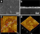
도 2는 본 발명의 일실시예에 따른 기판 위에 코팅된 산화 그라핀 층의 표면을 관찰한 SEM 사진이다(a: 기판 위의 산화 그라핀 층; b: 산화 그라핀 층의 단면; c: 산화 그라핀 층의 AFM 이미지; 및 d: 산화 그라핀 층의 3D 위상 AFM 이미지).
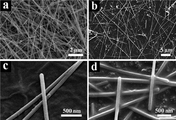
도 3은 본 발명에 따른 은 나노와이어의 SEM 사진이다(a: 폴리올 공정으로 합성된 은 나노와이어; b: 산화 그라핀 층 위의 은 나노와이어 네트워크; c: 열처리 전 은 나노와이어; 및 d: 열처리 후의 은 나노와이어).
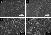
도 4는 본 발명의 일실시예에 따른 다양한 기판 위에 코팅된 산화 그라핀 층의 SEM 사진이다(a: 석영 기판; b: 유리 기판, c: 석영 기판 위의 산화 그라핀/은 나노와이어 네트워크 하이브리드 필름; 및 d: 유리 기판 위의 산화 그라핀/은 나노와이어 네트워크 하이브리드 필름).
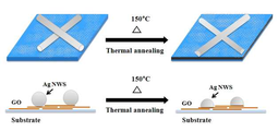
도 5는 본 발명에 따른 산화 그라핀/은 나노와이어 하이브리드 필름의 열처리 효과를 도식화하여 나타낸 것이다.
도 6은 본 발명에 따른 산화 그라핀/은 나노와이어 하이브리드 필름의 XP 스펙트라이다(a: C 1s XP 스펙트라; 및 b: Ag 3d XP 스펙트라).
도 7은 본 발명의 일실시예에 따른 다양한 기판 위의 산화 그라핀/은 나노와이어 하이브리드 필름의 UV-Vis 스펙트라이다(a: 석영 기판; b: 유리 기판; 및 c: PET 기판).
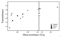
도 8은 본 발명의 일실시예에 따른 다양한 기판 위의 산화 그라핀/은 나노와이어 하이브리드 필름의 550 ㎚에서의 투광도 및 시트저항을 나타낸 것이다.
도 9는 본 발명에 따른 산화 그라핀/은 나노와이어 하이브리드 필름의 벤딩 횟수에 대한 시트저항을 나타낸 것이다.
도 10은 본 발명에 따른 산화 그라핀/은 나노와이어 하이브리드 필름의 열처리 전후의 기계적 안정성을 확인한 사진이다.

| 종류 | 시트저항 (Ω/sq) |
투과도 (%) |
σDC/σOP | 참고문헌 | |||
| 환원된 산화그라핀 |
화학적 환원 | 11300 | 87 | 0.29 | Zhu et al, APL 95, 103104 |
||
| 화학적 환원 | 30000 | 80 | 0.05 | Liu et al, Nanotechnology 20, 465605 |
|||
| 고온 | 5 K-1 M | 80 | 0.63 | Wu et al, APL 92, 263302 |
|||
| 고온 | 100-1000 | 80 | 1.6 | Becerril et al, ACS Nano 2, 463 |
|||
| 고온 | 8000 | 70 | 0.132 | Zhao etal, Electrochimica Acta, 55, 491 |
|||
| 고온 | 800 | 82 | 1.5 | Wu et al, ACS Nano, 4, 43 |
|||
| 화학적 환원 + 고온 |
100000 | 65 | 0.022 | Eda et al, Nature Nanotechnology, 3, 270 |
|||
| 화학적 환원 + 고온 |
11×106 | 95 | 0.03 | Kim et al, Langmuir, 25, 11302 |
|||
| 화학적 환원 + 고온 |
70000 | 65 | 0.011 | Eda et al, APL 92, 233305 |
|||
| 랭뮤어- 블로젯 증착 |
화학적 환원 + 고온 |
459 | 90 | 7.29 | Qingbin et al, ACS NANO, 5, 6039-6051 | ||
| 온도 | 4×10⁶ | 95 | 0.0018 | Kim et al. Adv. Mater. 2010, 22, 1954 |
|||
| 팽창(with DMF) | 1.5×10⁵ | 92 | 0.03 | Li et al. Nature Nanotechnol. 2008, 3, 538 |
|||
| 용액팽창 | 팽창(with DMF) | 5000 | 90 | 0.697 | Blake et al, Nano Letters, 8, 1704 |
||
| 팽창(with NaCl) | 2000 | 75 | 0.6 | Green et al , Nano Letters, 9,4031 |
|||
| 팽창(with DMF) | 8000 | 83 | 0.18 | Li et al, Nature Nanotechnology, 3, 538 |
|||
| CVD | Cu 기판 | 200 | 85 | 11.13 | Cai et al, APL 95, 123115 |
||
| Cu 기판 | 350 | 90 | 9.96 | Li et al, Nano Letters, 9,4359 |
|||
| Ni 기판 | 280 | 80 | 4.6 | Kim et al, Nature 457, 706 |
|||
| Ni 기판 | 770-1000 | 90 | 4.53 | Reina et al, Nano Letters, 9, 30 |
|||
| Ni 기판 | 1350-210 | 91-72 | 5.0 | Wang et al, APL, 95, 063302 |
|||
| 은 나노와이어 | 분사 | 33 | 85 | 75-350 | Anuj et al, Nanotechnology, 22 | ||
| 막대코팅 | 175 | 75 | 7.16 | Cai-Hong et al, Nano Res letter, 6, 75 | |||
| 건식 전이 | 10 | 85 | 222 | Anuj et al, Nano Res 3, 564-573 | |||
| 산화그라핀/은 나노와이어 | 하이브리드 | 150 | 87 | 20.9-90 | 본 발명 | ||
Claims (12)
- 산화 그라핀/은 나노와이어 하이브리드 투명전도성 필름.
- 제 1항에 있어서,
상기 투명전도성 필름은 투과도가 80~90%일 때, 면저항이 40~200 Ω/□인 것이 특징으로 하는 산화 그라핀/은 나노와이어 하이브리드 투명전도성 필름.
- (1) 나노 두께의 산화 그라핀 필름을 제조하는 단계;
(2) 폴리비닐피롤리돈(PVP) 존재 하에 에틸렌글리콜을 이용하여 질산은을 환원시켜 은 나노와이어를 제조하는 단계; 및
(3) 상기 (2) 단계에서 제조한 은 나노와이어를 상기 (1) 단계에서 제조한 산화 그라핀 필름 위에 부착하는 단계;
(4) 상기 (3) 단계에서 제조된 은 나노와이어 네트워크를 포함하는 산화 그라핀 필름을 건조시켜 투명전도성 필름을 제조하는 단계; 및
(5) 상기 투명전도성 필름을 열처리(thermal annealing)하는 단계;를 포함하는 것을 특징으로 하는 산화 그라핀/은 나노와이어 하이브리드 투명전도성 필름 제조방법.
- 제3항에 있어서,
상기 나노 두께의 산화 그라핀 필름은 모세관 유동을 구동력으로 이용하여 제조하는 것을 특징으로 하는 산화 그라핀/은 나노와이어 하이브리드 투명전도성 필름 제조방법.
- 제3항에 있어서,
상기 나노 두께의 그라핀 필름은,
(a) 천연 흑연을 동결건조하는 단계;
(b) 상기 동결건조된 천연 흑연을 초음파 처리를 통해 박리시켜 현탁액을 제조하는 단계; 및
(c) 상기 산화 그라핀 현탁액을 기판 위에 코팅하는 단계;를 포함하여 제조하는 것을 특징으로 하는 산화 그라핀/은 나노와이어 하이브리드 투명전도성 필름 제조방법.
- 제5항에 있어서,
상기 (a) 단계에서는, 천연 흑연으로부터 현탁액을 제조하여 액체 질소로 동결시킨 후, -50℃, 0.04~0.05 mbar의 동결건조기에서 72시간 동안 동결건조하는 것을 특징으로 하는 산화 그라핀/은 나노와이어 하이브리드 투명전도성 필름 제조방법.
- 제5항에 있어서,
상기 (b) 단계에서는, 상기 (a) 단계에서 얻은 산화 그라핀 파우더를 증류수에 넣고 초음파처리를 통해 박리시켜 0.0001~0.0003중량% 농도의 산화 그라핀 현탁액을 제조하는 것을 특징으로 하는 산화 그라핀/은 나노와이어 하이브리드 투명전도성 필름 제조방법.
- 제5항에 있어서,
상기 (c) 단계에서는, 상기 (b) 단계에서 얻은 산화 그라핀 현탁액을 유리, 석영 및 폴리에틸렌프탈레이트(PET)에서 선택되는 어느 하나의 기판 위에 코팅 후 건조하여 10~50 ㎚ 두께의 산화 그라핀 필름을 얻는 것을 특징으로 하는 산화 그라핀/은 나노와이어 하이브리드 투명전도성 필름 제조방법.
- 제3항에 있어서,
상기 은 나노와이어는 폴리올 공정(polyol process)을 이용하여 제조하는 것이 특징으로 하는 산화 그라핀/은 나노와이어 하이브리드 투명전도성 필름 제조방법.
- 제9항에 있어서,
상기 은 나노와이어의 평균 길이는 1~10 ㎛이고, 평균 직경은 70~80 ㎚인 것을 특징으로 하는 산화 그라핀/은 나노와이어 하이브리드 투명전도성 필름 제조방법.
- 제3항에 있어서,
상기 은 나노와이어는 상기 산화 그라핀 필름 위에 딥 코팅 방법을 이용하여 부착시키는 것을 특징으로 하는 산화 그라핀/은 나노와이어 하이브리드 투명전도성 필름 제조방법.
- 제3항에 있어서,
상기 투명전도성 필름은 산소분위기에서 150℃에서 30분간 열처리(thermal annealing)를 하는 것을 특징으로 하는 산화 그라핀/은 나노와이어 하이브리드 투명전도성 필름 제조방법.
Priority Applications (1)
| Application Number | Priority Date | Filing Date | Title |
|---|---|---|---|
| KR1020120026780A KR101324281B1 (ko) | 2012-03-15 | 2012-03-15 | 고유연성을 가지는 산화 그라핀/은 나노와이어 하이브리드를 기반으로 하는 투명전도성 필름 |
Applications Claiming Priority (1)
| Application Number | Priority Date | Filing Date | Title |
|---|---|---|---|
| KR1020120026780A KR101324281B1 (ko) | 2012-03-15 | 2012-03-15 | 고유연성을 가지는 산화 그라핀/은 나노와이어 하이브리드를 기반으로 하는 투명전도성 필름 |
Publications (2)
| Publication Number | Publication Date |
|---|---|
| KR20130104867A true KR20130104867A (ko) | 2013-09-25 |
| KR101324281B1 KR101324281B1 (ko) | 2013-11-01 |
Family
ID=49453625
Family Applications (1)
| Application Number | Title | Priority Date | Filing Date |
|---|---|---|---|
| KR1020120026780A Expired - Fee Related KR101324281B1 (ko) | 2012-03-15 | 2012-03-15 | 고유연성을 가지는 산화 그라핀/은 나노와이어 하이브리드를 기반으로 하는 투명전도성 필름 |
Country Status (1)
| Country | Link |
|---|---|
| KR (1) | KR101324281B1 (ko) |
Cited By (12)
| Publication number | Priority date | Publication date | Assignee | Title |
|---|---|---|---|---|
| CN104259475A (zh) * | 2014-09-24 | 2015-01-07 | 江苏大学 | 一种纳米银/石墨烯衍生物表面增强拉曼基体的制备方法 |
| WO2015102402A1 (ko) * | 2013-12-30 | 2015-07-09 | 엘지디스플레이 주식회사 | 멀티-기능 배리어층을 갖는 플렉서블 전자 디바이스 |
| WO2015102403A1 (ko) * | 2013-12-30 | 2015-07-09 | 엘지디스플레이 주식회사 | 멀티-기능 배리어층을 갖는 플렉서블 전자 디바이스 |
| KR101540030B1 (ko) * | 2014-06-16 | 2015-07-30 | 인하대학교 산학협력단 | Ag가 코팅된 그래핀나노플레이트 및 이의 제조방법 |
| CN104934109A (zh) * | 2015-06-03 | 2015-09-23 | 林州市清华·红旗渠新材料产业化发展中心 | 玻璃基底石墨烯/银纳米线透明导电薄膜的制备方法 |
| EP2963462A1 (en) * | 2014-06-30 | 2016-01-06 | LG Display Co., Ltd. | Transparent conductive layer, method for manufacturing the same and display device including the same |
| CN106371664A (zh) * | 2016-08-31 | 2017-02-01 | 焦祝根 | 一种柔性纳米触控膜的制备方法 |
| CN106683740A (zh) * | 2017-03-16 | 2017-05-17 | 西北大学 | 水热法石墨烯包覆银粉的制备及石墨烯包覆银粉改性无铅浆料的制备方法 |
| US10478899B2 (en) * | 2014-06-11 | 2019-11-19 | National Tsing Hua University | Method of making a transparent conductive composite material |
| CN111313240A (zh) * | 2020-02-29 | 2020-06-19 | 安徽艾瑞环境科技有限公司 | 平板石墨烯高能离子芯装置及其制作方法 |
| KR20210044042A (ko) * | 2019-10-14 | 2021-04-22 | 단국대학교 천안캠퍼스 산학협력단 | 염기성 용액 분사 공정을 통해 전도성이 향상된 투명 전도성 전극 필름의 제조 방법 |
| CN118834575A (zh) * | 2024-08-22 | 2024-10-25 | 哈尔滨工业大学 | 一种具有自感知除冰特性薄膜及其制备方法 |
Families Citing this family (4)
| Publication number | Priority date | Publication date | Assignee | Title |
|---|---|---|---|---|
| KR20160102783A (ko) | 2015-02-23 | 2016-08-31 | 한국교통대학교산학협력단 | 유연성 투명 전도성 필름 제조방법 및 이에 의해 제조된 유연성 투명 전도성 필름 |
| KR101892919B1 (ko) | 2016-12-09 | 2018-08-29 | 경북대학교 산학협력단 | 투명 하이브리드 전극 및 그 제조방법 |
| KR102491964B1 (ko) | 2022-06-20 | 2023-01-26 | 주식회사 도프 | 전도성 금속입자 에멀젼 액적의 커피링 현상을 이용하여 제조된 전도성 필름 |
| KR20240095805A (ko) | 2022-12-19 | 2024-06-26 | 주식회사 도프 | 전기적, 광학적 성능이 우수한 투명 전도성 필름 제조방법. |
Family Cites Families (1)
| Publication number | Priority date | Publication date | Assignee | Title |
|---|---|---|---|---|
| CN103777417B (zh) * | 2007-04-20 | 2017-01-18 | 凯姆控股有限公司 | 复合透明导体及其形成方法 |
-
2012
- 2012-03-15 KR KR1020120026780A patent/KR101324281B1/ko not_active Expired - Fee Related
Cited By (17)
| Publication number | Priority date | Publication date | Assignee | Title |
|---|---|---|---|---|
| WO2015102402A1 (ko) * | 2013-12-30 | 2015-07-09 | 엘지디스플레이 주식회사 | 멀티-기능 배리어층을 갖는 플렉서블 전자 디바이스 |
| WO2015102403A1 (ko) * | 2013-12-30 | 2015-07-09 | 엘지디스플레이 주식회사 | 멀티-기능 배리어층을 갖는 플렉서블 전자 디바이스 |
| US10478899B2 (en) * | 2014-06-11 | 2019-11-19 | National Tsing Hua University | Method of making a transparent conductive composite material |
| KR101540030B1 (ko) * | 2014-06-16 | 2015-07-30 | 인하대학교 산학협력단 | Ag가 코팅된 그래핀나노플레이트 및 이의 제조방법 |
| EP2963462A1 (en) * | 2014-06-30 | 2016-01-06 | LG Display Co., Ltd. | Transparent conductive layer, method for manufacturing the same and display device including the same |
| CN105225727A (zh) * | 2014-06-30 | 2016-01-06 | 乐金显示有限公司 | 透明导电层、用于制造其的方法及包括其的显示装置 |
| US10627932B2 (en) | 2014-06-30 | 2020-04-21 | Lg Display Co., Ltd. | Transparent conductive layer, method for manufacturing the same and display device including the same |
| CN104259475A (zh) * | 2014-09-24 | 2015-01-07 | 江苏大学 | 一种纳米银/石墨烯衍生物表面增强拉曼基体的制备方法 |
| CN104259475B (zh) * | 2014-09-24 | 2017-06-27 | 江苏大学 | 一种纳米银/石墨烯衍生物表面增强拉曼基体的制备方法 |
| CN104934109A (zh) * | 2015-06-03 | 2015-09-23 | 林州市清华·红旗渠新材料产业化发展中心 | 玻璃基底石墨烯/银纳米线透明导电薄膜的制备方法 |
| CN104934109B (zh) * | 2015-06-03 | 2018-09-11 | 林州市清华·红旗渠新材料产业化发展中心 | 玻璃基底石墨烯/银纳米线透明导电薄膜的制备方法 |
| CN106371664B (zh) * | 2016-08-31 | 2020-03-24 | 绍兴市梓昂新材料有限公司 | 一种柔性纳米触控膜的制备方法 |
| CN106371664A (zh) * | 2016-08-31 | 2017-02-01 | 焦祝根 | 一种柔性纳米触控膜的制备方法 |
| CN106683740A (zh) * | 2017-03-16 | 2017-05-17 | 西北大学 | 水热法石墨烯包覆银粉的制备及石墨烯包覆银粉改性无铅浆料的制备方法 |
| KR20210044042A (ko) * | 2019-10-14 | 2021-04-22 | 단국대학교 천안캠퍼스 산학협력단 | 염기성 용액 분사 공정을 통해 전도성이 향상된 투명 전도성 전극 필름의 제조 방법 |
| CN111313240A (zh) * | 2020-02-29 | 2020-06-19 | 安徽艾瑞环境科技有限公司 | 平板石墨烯高能离子芯装置及其制作方法 |
| CN118834575A (zh) * | 2024-08-22 | 2024-10-25 | 哈尔滨工业大学 | 一种具有自感知除冰特性薄膜及其制备方法 |
Also Published As
| Publication number | Publication date |
|---|---|
| KR101324281B1 (ko) | 2013-11-01 |
Similar Documents
| Publication | Publication Date | Title |
|---|---|---|
| KR101324281B1 (ko) | 고유연성을 가지는 산화 그라핀/은 나노와이어 하이브리드를 기반으로 하는 투명전도성 필름 | |
| Yun et al. | Transparent conducting films based on graphene oxide/silver nanowire hybrids with high flexibility | |
| Wang et al. | Tannic acid modified graphene/CNT three-dimensional conductive network for preparing high-performance transparent flexible heaters | |
| JP5748606B2 (ja) | 導電性塗料 | |
| Miao et al. | Low-temperature nanowelding ultrathin silver nanowire sandwiched between polydopamine-functionalized graphene and conjugated polymer for highly stable and flexible transparent electrodes | |
| EP2253001B1 (en) | Carbon nanotube-transparent conductive inorganic nanoparticles hybrid thin films for transparent conductive applications | |
| Yin et al. | Facile synthesis of oxidation‐resistant copper nanowires toward solution‐processable, flexible, foldable, and free‐standing electrodes | |
| CN102612490B (zh) | 含有石墨烯片和石墨的聚合物组合物 | |
| KR102120534B1 (ko) | 용액-가공성 금속 산화물 완충 층을 포함하는 광전자 장치 | |
| US20070246689A1 (en) | Transparent thin polythiophene films having improved conduction through use of nanomaterials | |
| US20150024122A1 (en) | Graphene ink and method for manufacturing graphene pattern using the same | |
| EP1914781A2 (en) | Transparent carbon nanotube electrode using conductive dispersant and production method thereof | |
| KR20150085523A (ko) | 그래핀 소재와 전도성 중합체를 포함한 막 형성용 조성물 | |
| Stevens et al. | Thermoelectric performance improvement of polymer nanocomposites by selective thermal degradation | |
| US20150083466A1 (en) | Method For The Functionalisation Of Metal Nanowires And The Production Of Electrodes | |
| Ahn et al. | Flexible metal nanowire-parylene C transparent electrodes for next generation optoelectronic devices | |
| KR101371289B1 (ko) | 탄소 나노박막의 제조방법 | |
| Chen et al. | Ultrahigh power output and durable flexible all-polymer triboelectric nanogenerators enabled by rational surface engineering | |
| TWI638463B (zh) | 透明導電膜、染料敏化太陽能電池用光電極及觸控面板以及染料敏化太陽能電池 | |
| KR101741334B1 (ko) | Gppv/rgo 이중층을 포함하는 다층박막의 제조방법 | |
| KR20130016846A (ko) | 우수한 면저항을 갖는 그래핀 투명 전극 및 이를 제조하는 방법 | |
| Fan et al. | A novel method of fabricating flexible transparent conductive large area graphene film | |
| Oh et al. | Fabrication of high-performance graphene nanoplatelet-based transparent electrodes via self-interlayer-exfoliation control | |
| Soon Choi et al. | Reduced graphite oxide-indium tin oxide hybrid materials for use as a transparent electrode | |
| Lee et al. | Highly efficient polymer light-emitting diodes using graphene oxide-modified flexible single-walled carbon nanotube electrodes |
Legal Events
| Date | Code | Title | Description |
|---|---|---|---|
| A201 | Request for examination | ||
| PA0109 | Patent application |
St.27 status event code: A-0-1-A10-A12-nap-PA0109 |
|
| PA0201 | Request for examination |
St.27 status event code: A-1-2-D10-D11-exm-PA0201 |
|
| D13-X000 | Search requested |
St.27 status event code: A-1-2-D10-D13-srh-X000 |
|
| D14-X000 | Search report completed |
St.27 status event code: A-1-2-D10-D14-srh-X000 |
|
| E902 | Notification of reason for refusal | ||
| PE0902 | Notice of grounds for rejection |
St.27 status event code: A-1-2-D10-D21-exm-PE0902 |
|
| E13-X000 | Pre-grant limitation requested |
St.27 status event code: A-2-3-E10-E13-lim-X000 |
|
| P11-X000 | Amendment of application requested |
St.27 status event code: A-2-2-P10-P11-nap-X000 |
|
| P13-X000 | Application amended |
St.27 status event code: A-2-2-P10-P13-nap-X000 |
|
| PG1501 | Laying open of application |
St.27 status event code: A-1-1-Q10-Q12-nap-PG1501 |
|
| E701 | Decision to grant or registration of patent right | ||
| PE0701 | Decision of registration |
St.27 status event code: A-1-2-D10-D22-exm-PE0701 |
|
| GRNT | Written decision to grant | ||
| PR0701 | Registration of establishment |
St.27 status event code: A-2-4-F10-F11-exm-PR0701 |
|
| PR1002 | Payment of registration fee |
Fee payment year number: 1 St.27 status event code: A-2-2-U10-U11-oth-PR1002 |
|
| PG1601 | Publication of registration |
St.27 status event code: A-4-4-Q10-Q13-nap-PG1601 |
|
| PN2301 | Change of applicant |
St.27 status event code: A-5-5-R10-R11-asn-PN2301 St.27 status event code: A-5-5-R10-R13-asn-PN2301 |
|
| P22-X000 | Classification modified |
St.27 status event code: A-4-4-P10-P22-nap-X000 |
|
| PN2301 | Change of applicant |
St.27 status event code: A-5-5-R10-R11-asn-PN2301 St.27 status event code: A-5-5-R10-R13-asn-PN2301 |
|
| PR1001 | Payment of annual fee |
Fee payment year number: 4 St.27 status event code: A-4-4-U10-U11-oth-PR1001 |
|
| FPAY | Annual fee payment |
Payment date: 20170829 Year of fee payment: 5 |
|
| PR1001 | Payment of annual fee |
Fee payment year number: 5 St.27 status event code: A-4-4-U10-U11-oth-PR1001 |
|
| R18-X000 | Changes to party contact information recorded |
St.27 status event code: A-5-5-R10-R18-oth-X000 |
|
| FPAY | Annual fee payment |
Payment date: 20180823 Year of fee payment: 6 |
|
| PR1001 | Payment of annual fee |
Fee payment year number: 6 St.27 status event code: A-4-4-U10-U11-oth-PR1001 |
|
| R18-X000 | Changes to party contact information recorded |
St.27 status event code: A-5-5-R10-R18-oth-X000 |
|
| PN2301 | Change of applicant |
St.27 status event code: A-5-5-R10-R11-asn-PN2301 |
|
| PN2301 | Change of applicant |
St.27 status event code: A-5-5-R10-R14-asn-PN2301 |
|
| P14-X000 | Amendment of ip right document requested |
St.27 status event code: A-5-5-P10-P14-nap-X000 |
|
| P16-X000 | Ip right document amended |
St.27 status event code: A-5-5-P10-P16-nap-X000 |
|
| Q16-X000 | A copy of ip right certificate issued |
St.27 status event code: A-4-4-Q10-Q16-nap-X000 |
|
| FPAY | Annual fee payment |
Payment date: 20191023 Year of fee payment: 7 |
|
| PR1001 | Payment of annual fee |
Fee payment year number: 7 St.27 status event code: A-4-4-U10-U11-oth-PR1001 |
|
| PC1903 | Unpaid annual fee |
Not in force date: 20201026 Payment event data comment text: Termination Category : DEFAULT_OF_REGISTRATION_FEE St.27 status event code: A-4-4-U10-U13-oth-PC1903 |
|
| PC1903 | Unpaid annual fee |
Ip right cessation event data comment text: Termination Category : DEFAULT_OF_REGISTRATION_FEE Not in force date: 20201026 St.27 status event code: N-4-6-H10-H13-oth-PC1903 |
|
| P22-X000 | Classification modified |
St.27 status event code: A-4-4-P10-P22-nap-X000 |
|
| P22-X000 | Classification modified |
St.27 status event code: A-4-4-P10-P22-nap-X000 |
|
| R18-X000 | Changes to party contact information recorded |
St.27 status event code: A-5-5-R10-R18-oth-X000 |