KR20130141032A - 광경화성 수지 이용 칩 제조방법 및 이의 전극 세척방법 - Google Patents
광경화성 수지 이용 칩 제조방법 및 이의 전극 세척방법 Download PDFInfo
- Publication number
- KR20130141032A KR20130141032A KR1020120064103A KR20120064103A KR20130141032A KR 20130141032 A KR20130141032 A KR 20130141032A KR 1020120064103 A KR1020120064103 A KR 1020120064103A KR 20120064103 A KR20120064103 A KR 20120064103A KR 20130141032 A KR20130141032 A KR 20130141032A
- Authority
- KR
- South Korea
- Prior art keywords
- electrode
- microchannel
- chip
- cleaning
- microchip
- Prior art date
- Legal status (The legal status is an assumption and is not a legal conclusion. Google has not performed a legal analysis and makes no representation as to the accuracy of the status listed.)
- Ceased
Links
Images


Classifications
-
- H—ELECTRICITY
- H10—SEMICONDUCTOR DEVICES; ELECTRIC SOLID-STATE DEVICES NOT OTHERWISE PROVIDED FOR
- H10P—GENERIC PROCESSES OR APPARATUS FOR THE MANUFACTURE OR TREATMENT OF DEVICES COVERED BY CLASS H10
- H10P70/00—Cleaning of wafers, substrates or parts of devices
- H10P70/20—Cleaning during device manufacture
Landscapes
- Micromachines (AREA)
Abstract
Description
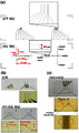
도 2는 본 발명의 일 실시예에 따른 전극 및 마이크로 채널의 고안을 나타낸 도이다. (a)는 전극 및 마이크로 채널 패턴을 위한 포토-마스크 디자인을 나타낸 것으로, 규모는 하기와 같다: 주입채널, 시료(및 시료-폐액) 저장소(sample(and sample-waste) reservoir)로부터 이중-T 채널까지 6 mm, 완충액 저장소로부터 이중-T 채널까지 2 mm; 분리채널 길이. 16 mm; 유효 길이, 12 mm; PGSB 채널, 350 μm. (b)는 전극과 마이크로칩 채널의 이미지를 나타낸 도이다. 채널의 너비 80 μm, 깊이 15 μm 이다. 이중-T 채널의 규모는 너비 80 μm, 깊이 15 μm 이며 100 μm의 주입교차점(injection intersection)을 포함한다. PGSB 채널은 120 μm 너비, 15 μm 깊이를 갖는다. Au 전극은 10 또는 20 μm의 폭을 갖는다. (c)는 채널-내 전기화학적 검출을 위한 마이크로칩 사진이다.
도 3은 전기화학적 세척 후 실험에 의해 계산된 전극의 면적과 이미지 촬영을 통해 얻은 전극면적을 비교한 도이다.
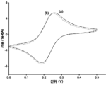
도 4는 0.5 M H2SO4로의 전기화학적 세척 효과를 나타낸 도이다. (a)와 (b)는 각각 H2SO4로의 전기화학적 세척 전과 후 Au 디스크 전극의 순환 전압전류도이다. Au 작업전극 너비는 10 μm 이며, 100 mM KNO3를 포함하는 5 mM K3Fe(CN)6 용액에서 50 mV/s의 주사속도로 Ag/AgCl에 대해 0과 +0.5 V 사이의 전위를 순환시킴으로 순환 전압전류법을 수행하였다.

Claims (14)
- 전극 및 마이크로채널을 구비한 칩으로서, 전극의 적어도 일부가 마이크로채널 내에 노출되어 있는 칩을 준비하는 제1단계;
마이크로채널을 통해 유기용매를 흘려주어 내부를 세척하는 제2단계; 및
산성용액으로 마이크로채널 내부에 노출된 전극표면을 전기화학적으로 세척하는 제3단계를 포함하는 칩의 제조방법.
- 제1항에 있어서,
상기 제2단계의 유기용매는 아세톤, 메탄올, 에탄올, n-프로판올, 이소프로판올 및 이의 혼합용매로 구성된 군으로부터 선택되는 것인 제조방법.
- 제1항에 있어서,
상기 제3단계는 마이크로 채널 내에 산성용액을 채우고 전극에 전압을 인가하는 순환전압전류법에 의해 마이크로채널 내부에 노출된 전극표면을 전기화학적으로 세척하는 것인 칩의 제조방법.
- 제1항에 있어서,
상기 칩은 전극이 패턴화된 제1기판과 마이크로채널이 패턴화된 제2기판을 접착시킨 것인 칩의 제조방법.
- 제3항에 있어서,
상기 제1기판과 제2기판의 접착은 광경화성 수지에 의한 것인 칩의 제조방법.
- 제3항에 있어서,
상기 세척단계는 상기 접착을 위해 사용된 반응물 및 이로부터 나온 부산물을 제거하는 것인 칩의 제조방법.
- 제1항에 있어서,
상기 전극은 포토리소그래피를 통해 전극물질을 증착시켜 형성된 것인 칩의 제조방법.
- 제6항에 있어서,
상기 전극물질은 금, 백금, 팔라듐, 은, 구리, 금속산화물, 탄소, ITO(indium tin oxide) 및 반도체성 물질로 구성된 군으로부터 선택되는 것인 칩의 제조방법.
- 제1항에 있어서,
상기 마이크로채널은 포토리소그래피를 수행한 후 습식 또는 건식 식각법에 의해 형성된 것인 칩의 제조방법.
- 제1항에 있어서,
상기 세척단계는 칩 제조시 사용되는 포토리소그래피 반응물 및 이로부터 나온 부산물 또는 칩 제조 후 마이크로채널 내부에 도입되는 구조물을 제작하기 위한 미반응 잔여물 및 이로부터 나온 반응부산물을 제거하는 것인 칩의 제조방법.
- 제1항에 있어서,
상기 산성용액의 pH는 1 내지 5인 것인 칩의 제조방법.
- 제1항에 있어서,
상기 전기화학적으로 세척하는 단계는 순환전압전류법(cyclic voltammetry; CV)에 의해 수행되는 것인 칩의 제조방법.
- 제1항 내지 제12항 중 어느 한 항에 있어서,
상기 칩은 마이크로칩 또는 나노칩인 것인 칩의 제조방법.
- 전극이 노출된 부분을 세척하는 방법에 있어서, 산성용액 중에서 전극에 전압을 인가하여 마이크로채널 내부에 노출된 전극표면을 전기화학적으로 세척하는 방법.
Priority Applications (1)
| Application Number | Priority Date | Filing Date | Title |
|---|---|---|---|
| KR1020120064103A KR20130141032A (ko) | 2012-06-15 | 2012-06-15 | 광경화성 수지 이용 칩 제조방법 및 이의 전극 세척방법 |
Applications Claiming Priority (1)
| Application Number | Priority Date | Filing Date | Title |
|---|---|---|---|
| KR1020120064103A KR20130141032A (ko) | 2012-06-15 | 2012-06-15 | 광경화성 수지 이용 칩 제조방법 및 이의 전극 세척방법 |
Publications (1)
| Publication Number | Publication Date |
|---|---|
| KR20130141032A true KR20130141032A (ko) | 2013-12-26 |
Family
ID=49985245
Family Applications (1)
| Application Number | Title | Priority Date | Filing Date |
|---|---|---|---|
| KR1020120064103A Ceased KR20130141032A (ko) | 2012-06-15 | 2012-06-15 | 광경화성 수지 이용 칩 제조방법 및 이의 전극 세척방법 |
Country Status (1)
| Country | Link |
|---|---|
| KR (1) | KR20130141032A (ko) |
Cited By (2)
| Publication number | Priority date | Publication date | Assignee | Title |
|---|---|---|---|---|
| WO2020065042A1 (fr) * | 2018-09-28 | 2020-04-02 | Klearia | Procédé de nettoyage et/ou de régénération d'un capteur microfluidique en verre pour l'analyse de métaux |
| WO2024207924A1 (zh) * | 2023-04-04 | 2024-10-10 | 广东粤港澳大湾区硬科技创新研究院 | 一种微通道板镀膜前的基板预处理方法 |
-
2012
- 2012-06-15 KR KR1020120064103A patent/KR20130141032A/ko not_active Ceased
Cited By (3)
| Publication number | Priority date | Publication date | Assignee | Title |
|---|---|---|---|---|
| WO2020065042A1 (fr) * | 2018-09-28 | 2020-04-02 | Klearia | Procédé de nettoyage et/ou de régénération d'un capteur microfluidique en verre pour l'analyse de métaux |
| FR3086554A1 (fr) * | 2018-09-28 | 2020-04-03 | Klearia | Procede de nettoyage et/ou de regeneration d'un capteur microfluidique en verre pour l'analyse de metaux |
| WO2024207924A1 (zh) * | 2023-04-04 | 2024-10-10 | 广东粤港澳大湾区硬科技创新研究院 | 一种微通道板镀膜前的基板预处理方法 |
Similar Documents
| Publication | Publication Date | Title |
|---|---|---|
| Childs et al. | Decal transfer microlithography: a new soft-lithographic patterning method | |
| RU2748273C9 (ru) | Подложка с наноотпечатком | |
| KR101402402B1 (ko) | 마이크로어레이 제작용 기판의 제조 방법 | |
| KR101409065B1 (ko) | 전기화학적 검출을 위한 전기영동칩 | |
| Silverio et al. | Microfabrication techniques for microfluidic devices | |
| Yu et al. | Oxygen reduction reaction induced pH-responsive chemo-mechanical hydrogel actuators | |
| EP1431018B1 (en) | Method of producing resin molded product | |
| Sudarsan et al. | Printed circuit technology for fabrication of plastic-based microfluidic devices | |
| KR20130141032A (ko) | 광경화성 수지 이용 칩 제조방법 및 이의 전극 세척방법 | |
| CN100503222C (zh) | 聚甲基丙烯酸甲酯微流控芯片溶剂辅助热压封装方法 | |
| Hemanth et al. | Pyrolytic 3D carbon microelectrodes for electrochemistry | |
| US8420181B2 (en) | Method of producing microfluidic devices based on a polymer | |
| Cheng et al. | Design and fabrication of a hybrid nanofluidic channel | |
| Mamun et al. | Patterning of platinum microelectrodes in polymeric microfluidic chips | |
| Lü et al. | Fabrication of high aspect ratio metallic microstructures on ITO glass substrate using reverse-side exposure of SU-8 | |
| JP4966694B2 (ja) | 微細構造金型の製造方法 | |
| Kole et al. | Rapid prototyping of nanofluidic slits in a silicone bilayer | |
| JP4944640B2 (ja) | 微細構造金型の製造方法 | |
| EP4458758A1 (en) | Microfluidic chip and method for manufacturing microfluidic chip | |
| CN119500296B (zh) | 一种集成偶联活性膜的数字微流控芯片及其制备方法和应用 | |
| Rossettini | YBAR resonators for biosensing Channels in Silicon | |
| Sayah et al. | LF55GN photosensitive flexopolymer: a new material for ultrathick and high-aspect-ratio MEMS fabrication | |
| JP4769544B2 (ja) | 二次鋳型の製造方法 | |
| Warfield | A Manufacturing Process for Interdigitated Microelectrodes on Glass Wafers | |
| KR100901195B1 (ko) | 플라스틱 기판 상의 미세 패턴 형성방법 |
Legal Events
| Date | Code | Title | Description |
|---|---|---|---|
| A201 | Request for examination | ||
| PA0109 | Patent application |
St.27 status event code: A-0-1-A10-A12-nap-PA0109 |
|
| PA0201 | Request for examination |
St.27 status event code: A-1-2-D10-D11-exm-PA0201 |
|
| P11-X000 | Amendment of application requested |
St.27 status event code: A-2-2-P10-P11-nap-X000 |
|
| P13-X000 | Application amended |
St.27 status event code: A-2-2-P10-P13-nap-X000 |
|
| R18-X000 | Changes to party contact information recorded |
St.27 status event code: A-3-3-R10-R18-oth-X000 |
|
| E902 | Notification of reason for refusal | ||
| PE0902 | Notice of grounds for rejection |
St.27 status event code: A-1-2-D10-D21-exm-PE0902 |
|
| T11-X000 | Administrative time limit extension requested |
St.27 status event code: U-3-3-T10-T11-oth-X000 |
|
| T11-X000 | Administrative time limit extension requested |
St.27 status event code: U-3-3-T10-T11-oth-X000 |
|
| E13-X000 | Pre-grant limitation requested |
St.27 status event code: A-2-3-E10-E13-lim-X000 |
|
| P11-X000 | Amendment of application requested |
St.27 status event code: A-2-2-P10-P11-nap-X000 |
|
| P13-X000 | Application amended |
St.27 status event code: A-2-2-P10-P13-nap-X000 |
|
| PG1501 | Laying open of application |
St.27 status event code: A-1-1-Q10-Q12-nap-PG1501 |
|
| E601 | Decision to refuse application | ||
| PE0601 | Decision on rejection of patent |
St.27 status event code: N-2-6-B10-B15-exm-PE0601 |
|
| T11-X000 | Administrative time limit extension requested |
St.27 status event code: U-3-3-T10-T11-oth-X000 |
|
| PN2301 | Change of applicant |
St.27 status event code: A-3-3-R10-R13-asn-PN2301 St.27 status event code: A-3-3-R10-R11-asn-PN2301 |
|
| PN2301 | Change of applicant |
St.27 status event code: A-3-3-R10-R13-asn-PN2301 St.27 status event code: A-3-3-R10-R11-asn-PN2301 |
|
| P22-X000 | Classification modified |
St.27 status event code: A-2-2-P10-P22-nap-X000 |
|
| P22-X000 | Classification modified |
St.27 status event code: A-2-2-P10-P22-nap-X000 |
|
| R18-X000 | Changes to party contact information recorded |
St.27 status event code: A-3-3-R10-R18-oth-X000 |
|
| R18-X000 | Changes to party contact information recorded |
St.27 status event code: A-3-3-R10-R18-oth-X000 |
|
| PN2301 | Change of applicant |
St.27 status event code: A-3-3-R10-R13-asn-PN2301 St.27 status event code: A-3-3-R10-R11-asn-PN2301 |
|
| PN2301 | Change of applicant |
St.27 status event code: A-3-3-R10-R13-asn-PN2301 St.27 status event code: A-3-3-R10-R11-asn-PN2301 |
|
| R18-X000 | Changes to party contact information recorded |
St.27 status event code: A-3-3-R10-R18-oth-X000 |
|
| R18-X000 | Changes to party contact information recorded |
St.27 status event code: A-3-3-R10-R18-oth-X000 |
|
| R18-X000 | Changes to party contact information recorded |
St.27 status event code: A-3-3-R10-R18-oth-X000 |
|
| R18-X000 | Changes to party contact information recorded |
St.27 status event code: A-3-3-R10-R18-oth-X000 |
|
| R18-X000 | Changes to party contact information recorded |
St.27 status event code: A-3-3-R10-R18-oth-X000 |
|
| R18-X000 | Changes to party contact information recorded |
St.27 status event code: A-3-3-R10-R18-oth-X000 |
|
| R18 | Changes to party contact information recorded |
Free format text: ST27 STATUS EVENT CODE: A-3-3-R10-R18-OTH-X000 (AS PROVIDED BY THE NATIONAL OFFICE) |
|
| R18-X000 | Changes to party contact information recorded |
St.27 status event code: A-3-3-R10-R18-oth-X000 |
|
| P22-X000 | Classification modified |
St.27 status event code: A-2-2-P10-P22-nap-X000 |