KR20130141387A - 집적 회로 패키지 및 그 제조 방법 - Google Patents
집적 회로 패키지 및 그 제조 방법 Download PDFInfo
- Publication number
- KR20130141387A KR20130141387A KR20130067968A KR20130067968A KR20130141387A KR 20130141387 A KR20130141387 A KR 20130141387A KR 20130067968 A KR20130067968 A KR 20130067968A KR 20130067968 A KR20130067968 A KR 20130067968A KR 20130141387 A KR20130141387 A KR 20130141387A
- Authority
- KR
- South Korea
- Prior art keywords
- die
- adhesive layer
- layer
- dielectric substrate
- adhesive
- Prior art date
- Legal status (The legal status is an assumption and is not a legal conclusion. Google has not performed a legal analysis and makes no representation as to the accuracy of the status listed.)
- Granted
Links
Images

















Classifications
-
- H—ELECTRICITY
- H10—SEMICONDUCTOR DEVICES; ELECTRIC SOLID-STATE DEVICES NOT OTHERWISE PROVIDED FOR
- H10W—GENERIC PACKAGES, INTERCONNECTIONS, CONNECTORS OR OTHER CONSTRUCTIONAL DETAILS OF DEVICES COVERED BY CLASS H10
- H10W90/00—Package configurations
-
- H—ELECTRICITY
- H10—SEMICONDUCTOR DEVICES; ELECTRIC SOLID-STATE DEVICES NOT OTHERWISE PROVIDED FOR
- H10W—GENERIC PACKAGES, INTERCONNECTIONS, CONNECTORS OR OTHER CONSTRUCTIONAL DETAILS OF DEVICES COVERED BY CLASS H10
- H10W42/00—Arrangements for protection of devices
-
- H—ELECTRICITY
- H10—SEMICONDUCTOR DEVICES; ELECTRIC SOLID-STATE DEVICES NOT OTHERWISE PROVIDED FOR
- H10P—GENERIC PROCESSES OR APPARATUS FOR THE MANUFACTURE OR TREATMENT OF DEVICES COVERED BY CLASS H10
- H10P72/00—Handling or holding of wafers, substrates or devices during manufacture or treatment thereof
- H10P72/70—Handling or holding of wafers, substrates or devices during manufacture or treatment thereof for supporting or gripping
- H10P72/74—Handling or holding of wafers, substrates or devices during manufacture or treatment thereof for supporting or gripping using temporarily an auxiliary support
- H10P72/7402—Wafer tapes, e.g. grinding or dicing support tapes
-
- H—ELECTRICITY
- H10—SEMICONDUCTOR DEVICES; ELECTRIC SOLID-STATE DEVICES NOT OTHERWISE PROVIDED FOR
- H10W—GENERIC PACKAGES, INTERCONNECTIONS, CONNECTORS OR OTHER CONSTRUCTIONAL DETAILS OF DEVICES COVERED BY CLASS H10
- H10W70/00—Package substrates; Interposers; Redistribution layers [RDL]
- H10W70/01—Manufacture or treatment
- H10W70/05—Manufacture or treatment of insulating or insulated package substrates, or of interposers, or of redistribution layers
-
- H—ELECTRICITY
- H10—SEMICONDUCTOR DEVICES; ELECTRIC SOLID-STATE DEVICES NOT OTHERWISE PROVIDED FOR
- H10W—GENERIC PACKAGES, INTERCONNECTIONS, CONNECTORS OR OTHER CONSTRUCTIONAL DETAILS OF DEVICES COVERED BY CLASS H10
- H10W70/00—Package substrates; Interposers; Redistribution layers [RDL]
- H10W70/01—Manufacture or treatment
- H10W70/05—Manufacture or treatment of insulating or insulated package substrates, or of interposers, or of redistribution layers
- H10W70/08—Manufacture or treatment of insulating or insulated package substrates, or of interposers, or of redistribution layers by depositing layers on the chip or wafer, e.g. "chip-first" RDLs
- H10W70/09—Manufacture or treatment of insulating or insulated package substrates, or of interposers, or of redistribution layers by depositing layers on the chip or wafer, e.g. "chip-first" RDLs extending onto an encapsulation that laterally surrounds the chip or wafer, e.g. fan-out wafer level package [FOWLP] RDLs
-
- H—ELECTRICITY
- H10—SEMICONDUCTOR DEVICES; ELECTRIC SOLID-STATE DEVICES NOT OTHERWISE PROVIDED FOR
- H10W—GENERIC PACKAGES, INTERCONNECTIONS, CONNECTORS OR OTHER CONSTRUCTIONAL DETAILS OF DEVICES COVERED BY CLASS H10
- H10W70/00—Package substrates; Interposers; Redistribution layers [RDL]
- H10W70/01—Manufacture or treatment
- H10W70/05—Manufacture or treatment of insulating or insulated package substrates, or of interposers, or of redistribution layers
- H10W70/095—Manufacture or treatment of insulating or insulated package substrates, or of interposers, or of redistribution layers of vias therein
-
- H—ELECTRICITY
- H10—SEMICONDUCTOR DEVICES; ELECTRIC SOLID-STATE DEVICES NOT OTHERWISE PROVIDED FOR
- H10W—GENERIC PACKAGES, INTERCONNECTIONS, CONNECTORS OR OTHER CONSTRUCTIONAL DETAILS OF DEVICES COVERED BY CLASS H10
- H10W70/00—Package substrates; Interposers; Redistribution layers [RDL]
- H10W70/60—Insulating or insulated package substrates; Interposers; Redistribution layers
-
- H—ELECTRICITY
- H10—SEMICONDUCTOR DEVICES; ELECTRIC SOLID-STATE DEVICES NOT OTHERWISE PROVIDED FOR
- H10W—GENERIC PACKAGES, INTERCONNECTIONS, CONNECTORS OR OTHER CONSTRUCTIONAL DETAILS OF DEVICES COVERED BY CLASS H10
- H10W70/00—Package substrates; Interposers; Redistribution layers [RDL]
- H10W70/60—Insulating or insulated package substrates; Interposers; Redistribution layers
- H10W70/611—Insulating or insulated package substrates; Interposers; Redistribution layers for connecting multiple chips together
-
- H—ELECTRICITY
- H10—SEMICONDUCTOR DEVICES; ELECTRIC SOLID-STATE DEVICES NOT OTHERWISE PROVIDED FOR
- H10W—GENERIC PACKAGES, INTERCONNECTIONS, CONNECTORS OR OTHER CONSTRUCTIONAL DETAILS OF DEVICES COVERED BY CLASS H10
- H10W70/00—Package substrates; Interposers; Redistribution layers [RDL]
- H10W70/60—Insulating or insulated package substrates; Interposers; Redistribution layers
- H10W70/62—Insulating or insulated package substrates; Interposers; Redistribution layers characterised by their interconnections
- H10W70/63—Vias, e.g. via plugs
- H10W70/635—Through-vias
-
- H—ELECTRICITY
- H10—SEMICONDUCTOR DEVICES; ELECTRIC SOLID-STATE DEVICES NOT OTHERWISE PROVIDED FOR
- H10W—GENERIC PACKAGES, INTERCONNECTIONS, CONNECTORS OR OTHER CONSTRUCTIONAL DETAILS OF DEVICES COVERED BY CLASS H10
- H10W70/00—Package substrates; Interposers; Redistribution layers [RDL]
- H10W70/60—Insulating or insulated package substrates; Interposers; Redistribution layers
- H10W70/62—Insulating or insulated package substrates; Interposers; Redistribution layers characterised by their interconnections
- H10W70/65—Shapes or dispositions of interconnections
-
- H—ELECTRICITY
- H10—SEMICONDUCTOR DEVICES; ELECTRIC SOLID-STATE DEVICES NOT OTHERWISE PROVIDED FOR
- H10W—GENERIC PACKAGES, INTERCONNECTIONS, CONNECTORS OR OTHER CONSTRUCTIONAL DETAILS OF DEVICES COVERED BY CLASS H10
- H10W70/00—Package substrates; Interposers; Redistribution layers [RDL]
- H10W70/60—Insulating or insulated package substrates; Interposers; Redistribution layers
- H10W70/67—Insulating or insulated package substrates; Interposers; Redistribution layers characterised by their insulating layers or insulating parts
- H10W70/68—Shapes or dispositions thereof
- H10W70/685—Shapes or dispositions thereof comprising multiple insulating layers
-
- H—ELECTRICITY
- H10—SEMICONDUCTOR DEVICES; ELECTRIC SOLID-STATE DEVICES NOT OTHERWISE PROVIDED FOR
- H10W—GENERIC PACKAGES, INTERCONNECTIONS, CONNECTORS OR OTHER CONSTRUCTIONAL DETAILS OF DEVICES COVERED BY CLASS H10
- H10W72/00—Interconnections or connectors in packages
- H10W72/30—Die-attach connectors
-
- H—ELECTRICITY
- H05—ELECTRIC TECHNIQUES NOT OTHERWISE PROVIDED FOR
- H05K—PRINTED CIRCUITS; CASINGS OR CONSTRUCTIONAL DETAILS OF ELECTRIC APPARATUS; MANUFACTURE OF ASSEMBLAGES OF ELECTRICAL COMPONENTS
- H05K3/00—Apparatus or processes for manufacturing printed circuits
- H05K3/30—Assembling printed circuits with electric components, e.g. with resistors
- H05K3/303—Assembling printed circuits with electric components, e.g. with resistors with surface mounted components
- H05K3/305—Affixing by adhesive
-
- H—ELECTRICITY
- H10—SEMICONDUCTOR DEVICES; ELECTRIC SOLID-STATE DEVICES NOT OTHERWISE PROVIDED FOR
- H10P—GENERIC PROCESSES OR APPARATUS FOR THE MANUFACTURE OR TREATMENT OF DEVICES COVERED BY CLASS H10
- H10P72/00—Handling or holding of wafers, substrates or devices during manufacture or treatment thereof
- H10P72/70—Handling or holding of wafers, substrates or devices during manufacture or treatment thereof for supporting or gripping
- H10P72/74—Handling or holding of wafers, substrates or devices during manufacture or treatment thereof for supporting or gripping using temporarily an auxiliary support
- H10P72/7416—Handling or holding of wafers, substrates or devices during manufacture or treatment thereof for supporting or gripping using temporarily an auxiliary support used during dicing or grinding
-
- H—ELECTRICITY
- H10—SEMICONDUCTOR DEVICES; ELECTRIC SOLID-STATE DEVICES NOT OTHERWISE PROVIDED FOR
- H10P—GENERIC PROCESSES OR APPARATUS FOR THE MANUFACTURE OR TREATMENT OF DEVICES COVERED BY CLASS H10
- H10P72/00—Handling or holding of wafers, substrates or devices during manufacture or treatment thereof
- H10P72/70—Handling or holding of wafers, substrates or devices during manufacture or treatment thereof for supporting or gripping
- H10P72/74—Handling or holding of wafers, substrates or devices during manufacture or treatment thereof for supporting or gripping using temporarily an auxiliary support
- H10P72/7422—Handling or holding of wafers, substrates or devices during manufacture or treatment thereof for supporting or gripping using temporarily an auxiliary support used to protect an active side of a device or wafer
-
- H—ELECTRICITY
- H10—SEMICONDUCTOR DEVICES; ELECTRIC SOLID-STATE DEVICES NOT OTHERWISE PROVIDED FOR
- H10P—GENERIC PROCESSES OR APPARATUS FOR THE MANUFACTURE OR TREATMENT OF DEVICES COVERED BY CLASS H10
- H10P72/00—Handling or holding of wafers, substrates or devices during manufacture or treatment thereof
- H10P72/70—Handling or holding of wafers, substrates or devices during manufacture or treatment thereof for supporting or gripping
- H10P72/74—Handling or holding of wafers, substrates or devices during manufacture or treatment thereof for supporting or gripping using temporarily an auxiliary support
- H10P72/744—Details of chemical or physical process used for separating the auxiliary support from a device or a wafer
-
- H—ELECTRICITY
- H10—SEMICONDUCTOR DEVICES; ELECTRIC SOLID-STATE DEVICES NOT OTHERWISE PROVIDED FOR
- H10W—GENERIC PACKAGES, INTERCONNECTIONS, CONNECTORS OR OTHER CONSTRUCTIONAL DETAILS OF DEVICES COVERED BY CLASS H10
- H10W70/00—Package substrates; Interposers; Redistribution layers [RDL]
- H10W70/01—Manufacture or treatment
- H10W70/05—Manufacture or treatment of insulating or insulated package substrates, or of interposers, or of redistribution layers
- H10W70/093—Connecting or disconnecting other interconnections thereto or therefrom, e.g. connecting bond wires or bumps
-
- H—ELECTRICITY
- H10—SEMICONDUCTOR DEVICES; ELECTRIC SOLID-STATE DEVICES NOT OTHERWISE PROVIDED FOR
- H10W—GENERIC PACKAGES, INTERCONNECTIONS, CONNECTORS OR OTHER CONSTRUCTIONAL DETAILS OF DEVICES COVERED BY CLASS H10
- H10W72/00—Interconnections or connectors in packages
- H10W72/01—Manufacture or treatment
- H10W72/013—Manufacture or treatment of die-attach connectors
- H10W72/01304—Manufacture or treatment of die-attach connectors using temporary auxiliary members, e.g. using sacrificial coatings or handle substrates
-
- H—ELECTRICITY
- H10—SEMICONDUCTOR DEVICES; ELECTRIC SOLID-STATE DEVICES NOT OTHERWISE PROVIDED FOR
- H10W—GENERIC PACKAGES, INTERCONNECTIONS, CONNECTORS OR OTHER CONSTRUCTIONAL DETAILS OF DEVICES COVERED BY CLASS H10
- H10W72/00—Interconnections or connectors in packages
- H10W72/01—Manufacture or treatment
- H10W72/013—Manufacture or treatment of die-attach connectors
- H10W72/01321—Manufacture or treatment of die-attach connectors using local deposition
- H10W72/01323—Manufacture or treatment of die-attach connectors using local deposition in liquid form, e.g. by dispensing droplets or by screen printing
-
- H—ELECTRICITY
- H10—SEMICONDUCTOR DEVICES; ELECTRIC SOLID-STATE DEVICES NOT OTHERWISE PROVIDED FOR
- H10W—GENERIC PACKAGES, INTERCONNECTIONS, CONNECTORS OR OTHER CONSTRUCTIONAL DETAILS OF DEVICES COVERED BY CLASS H10
- H10W72/00—Interconnections or connectors in packages
- H10W72/01—Manufacture or treatment
- H10W72/013—Manufacture or treatment of die-attach connectors
- H10W72/01331—Manufacture or treatment of die-attach connectors using blanket deposition
- H10W72/01333—Manufacture or treatment of die-attach connectors using blanket deposition in liquid form, e.g. spin coating, spray coating or immersion coating
-
- H—ELECTRICITY
- H10—SEMICONDUCTOR DEVICES; ELECTRIC SOLID-STATE DEVICES NOT OTHERWISE PROVIDED FOR
- H10W—GENERIC PACKAGES, INTERCONNECTIONS, CONNECTORS OR OTHER CONSTRUCTIONAL DETAILS OF DEVICES COVERED BY CLASS H10
- H10W72/00—Interconnections or connectors in packages
- H10W72/01—Manufacture or treatment
- H10W72/013—Manufacture or treatment of die-attach connectors
- H10W72/01331—Manufacture or treatment of die-attach connectors using blanket deposition
- H10W72/01336—Manufacture or treatment of die-attach connectors using blanket deposition in solid form, e.g. by using a powder or by laminating a foil
-
- H—ELECTRICITY
- H10—SEMICONDUCTOR DEVICES; ELECTRIC SOLID-STATE DEVICES NOT OTHERWISE PROVIDED FOR
- H10W—GENERIC PACKAGES, INTERCONNECTIONS, CONNECTORS OR OTHER CONSTRUCTIONAL DETAILS OF DEVICES COVERED BY CLASS H10
- H10W72/00—Interconnections or connectors in packages
- H10W72/01—Manufacture or treatment
- H10W72/013—Manufacture or treatment of die-attach connectors
- H10W72/01365—Thermally treating
-
- H—ELECTRICITY
- H10—SEMICONDUCTOR DEVICES; ELECTRIC SOLID-STATE DEVICES NOT OTHERWISE PROVIDED FOR
- H10W—GENERIC PACKAGES, INTERCONNECTIONS, CONNECTORS OR OTHER CONSTRUCTIONAL DETAILS OF DEVICES COVERED BY CLASS H10
- H10W72/00—Interconnections or connectors in packages
- H10W72/01—Manufacture or treatment
- H10W72/013—Manufacture or treatment of die-attach connectors
- H10W72/01371—Cleaning, e.g. oxide removal or de-smearing
-
- H—ELECTRICITY
- H10—SEMICONDUCTOR DEVICES; ELECTRIC SOLID-STATE DEVICES NOT OTHERWISE PROVIDED FOR
- H10W—GENERIC PACKAGES, INTERCONNECTIONS, CONNECTORS OR OTHER CONSTRUCTIONAL DETAILS OF DEVICES COVERED BY CLASS H10
- H10W72/00—Interconnections or connectors in packages
- H10W72/01—Manufacture or treatment
- H10W72/0198—Manufacture or treatment batch processes
-
- H—ELECTRICITY
- H10—SEMICONDUCTOR DEVICES; ELECTRIC SOLID-STATE DEVICES NOT OTHERWISE PROVIDED FOR
- H10W—GENERIC PACKAGES, INTERCONNECTIONS, CONNECTORS OR OTHER CONSTRUCTIONAL DETAILS OF DEVICES COVERED BY CLASS H10
- H10W72/00—Interconnections or connectors in packages
- H10W72/071—Connecting or disconnecting
- H10W72/073—Connecting or disconnecting of die-attach connectors
-
- H—ELECTRICITY
- H10—SEMICONDUCTOR DEVICES; ELECTRIC SOLID-STATE DEVICES NOT OTHERWISE PROVIDED FOR
- H10W—GENERIC PACKAGES, INTERCONNECTIONS, CONNECTORS OR OTHER CONSTRUCTIONAL DETAILS OF DEVICES COVERED BY CLASS H10
- H10W72/00—Interconnections or connectors in packages
- H10W72/071—Connecting or disconnecting
- H10W72/073—Connecting or disconnecting of die-attach connectors
- H10W72/07331—Connecting techniques
- H10W72/07337—Connecting techniques using a polymer adhesive, e.g. an adhesive based on silicone or epoxy
- H10W72/07338—Connecting techniques using a polymer adhesive, e.g. an adhesive based on silicone or epoxy hardening the adhesive by curing, e.g. thermosetting
-
- H—ELECTRICITY
- H10—SEMICONDUCTOR DEVICES; ELECTRIC SOLID-STATE DEVICES NOT OTHERWISE PROVIDED FOR
- H10W—GENERIC PACKAGES, INTERCONNECTIONS, CONNECTORS OR OTHER CONSTRUCTIONAL DETAILS OF DEVICES COVERED BY CLASS H10
- H10W72/00—Interconnections or connectors in packages
- H10W72/30—Die-attach connectors
- H10W72/351—Materials of die-attach connectors
- H10W72/353—Materials of die-attach connectors not comprising solid metals or solid metalloids, e.g. ceramics
- H10W72/354—Materials of die-attach connectors not comprising solid metals or solid metalloids, e.g. ceramics comprising polymers
-
- H—ELECTRICITY
- H10—SEMICONDUCTOR DEVICES; ELECTRIC SOLID-STATE DEVICES NOT OTHERWISE PROVIDED FOR
- H10W—GENERIC PACKAGES, INTERCONNECTIONS, CONNECTORS OR OTHER CONSTRUCTIONAL DETAILS OF DEVICES COVERED BY CLASS H10
- H10W72/00—Interconnections or connectors in packages
- H10W72/90—Bond pads, in general
- H10W72/941—Dispositions of bond pads
- H10W72/9413—Dispositions of bond pads on encapsulations
-
- H—ELECTRICITY
- H10—SEMICONDUCTOR DEVICES; ELECTRIC SOLID-STATE DEVICES NOT OTHERWISE PROVIDED FOR
- H10W—GENERIC PACKAGES, INTERCONNECTIONS, CONNECTORS OR OTHER CONSTRUCTIONAL DETAILS OF DEVICES COVERED BY CLASS H10
- H10W90/00—Package configurations
- H10W90/701—Package configurations characterised by the relative positions of pads or connectors relative to package parts
- H10W90/731—Package configurations characterised by the relative positions of pads or connectors relative to package parts of die-attach connectors
- H10W90/734—Package configurations characterised by the relative positions of pads or connectors relative to package parts of die-attach connectors between a chip and a stacked insulating package substrate, interposer or RDL
-
- H—ELECTRICITY
- H10—SEMICONDUCTOR DEVICES; ELECTRIC SOLID-STATE DEVICES NOT OTHERWISE PROVIDED FOR
- H10W—GENERIC PACKAGES, INTERCONNECTIONS, CONNECTORS OR OTHER CONSTRUCTIONAL DETAILS OF DEVICES COVERED BY CLASS H10
- H10W99/00—Subject matter not provided for in other groups of this subclass
Landscapes
- Die Bonding (AREA)
- Engineering & Computer Science (AREA)
- Manufacturing & Machinery (AREA)
- Physics & Mathematics (AREA)
- Geometry (AREA)
- Wire Bonding (AREA)
- Production Of Multi-Layered Print Wiring Board (AREA)
Abstract
Description
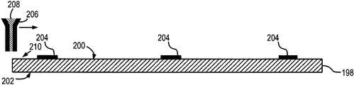
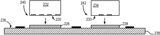
도 1 내지 도 7은 본 발명의 실시예에 따라 집적 칩 패키지를 제조하는 단계를 도시한 개략도이다.
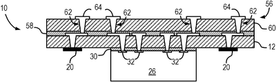
도 8은 본 발명의 실시예에 따른 집적 멀티칩 패키지의 단면도이다.
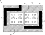
도 9는 도 8의 집적 멀티칩 패키지의 저면도이다.
도 10은 본 발명의 실시예에 따라 집적 칩 패키지를 제조하는 단계를 예시한 흐름도이다.
도 11은 본 발명의 실시예에 따른 웨이퍼 조립체의 저면도이다.
도 12는 도 11의 웨이퍼 조립체의 단면도이다.
도 13은 도 11의 웨이퍼 조립체에서 절단된 다이 조립체의 단면도이다.
도 14는 본 발명의 다른 실시예에 따라 집적 칩 패키지를 제조하는 단계를 예시한 흐름도이다.
도 15는 본 발명의 실시예에 따른 웨이퍼 조립체의 저면도이다.
도 16은 도 15의 웨이퍼 조립체의 단면도이다.
도 17은 도 15의 웨이퍼 조립체에서 절단된 다이 조립체의 단면도이다.
도 18은 본 발명의 또 다른 실시예에 따라 집적 칩 패키지를 제조하는 단계를 예시한 흐름도이다.
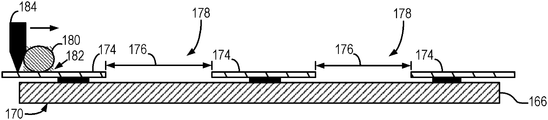
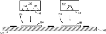
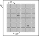
도 19 내지 도 24는 본 발명의 다른 실시예에 따라 집적 칩 패키지를 위한 빌드업 프로세스의 단계를 도시한 개략도이다.
도 25는 도 19 내지 도 24에서 설명된 실시예에 따라 접착제 층을 분배하는 데 사용되는 금속 스크린의 부분의 평면도이다.
도 26 내지 도 29는 본 발명의 다른 실시예에 따라 집적 칩 패키지를 위한 빌드업 프로세스의 단계를 도시한 개략도이다.
도 30은 본 발명의 실시예에 따라 접착제 층으로 코팅된 박리 시트(release sheet)의 평면도이다.
도 31은 접착제 층을 다이 크기로 스크라이브(scribe)한 후 도 30의 접착제 코팅된 박리 시트의 평면도이다.
도 32 내지 도 35는 본 발명의 또 다른 실시예에 따라 집적 칩 패키지의 빌드업 프로세스의 단계를 도시한 개략도이다.
Claims (35)
- 적어도 하나의 다이 패드가 배치된 활성 표면을 포함하는 제 1 다이와,
상기 제 1 다이의 상기 활성 표면에 결합된 제 1 표면 및 상기 제 1 표면과 대향하는 제 2 표면을 가진 제 1 접착제 층과,
상부 표면을 가지는 제 1 유전체 층 -상기 제 1 유전체 층의 상기 상부 표면의 제 1 부분은 상기 제 1 접착제 층의 상기 제 2 표면에 결합됨- 을 포함하되,
상기 제 1 부분과 다른, 상기 제 1 유전체 층의 상기 상부 표면의 제 2 부분은 실질적으로 접착제가 없는
칩 패키지.
- 제 1 항에 있어서,
상기 제 1 유전체 층의 상기 상부 표면의 상기 제 2 부분은 상기 유전체 층의 상기 상부 표면의 상기 제 1 부분을 실질적으로 둘러싸는
칩 패키지.
- 제 1 항에 있어서,
상기 제 1 접착제 층의 상기 제 1 표면은 상기 제 1 다이의 상기 활성 표면의 표면 영역과 거의 동일한
칩 패키지.
- 제 1 항에 있어서,
적어도 하나의 다이 패드가 배치된 활성 표면을 포함하는 제 2 다이와,
상기 제 2 다이의 상기 활성 표면에 결합된 제 1 표면 및 상기 제 1 표면과 대향하는 제 2 표면을 가진 제 2 접착제 층을 더 포함하되,
상기 제 2 접착제 층의 상기 제 2 표면은 상기 제 1 유전체 층의 상부 표면의 제 3 부분에 결합되는
칩 패키지.
- 제 4 항에 있어서,
상기 제 1 다이 및 상기 제 2 다이는 상기 제 1 다이와 상기 제 2 다이 사이에 갭(gap)이 형성되도록 배치되며,
상기 갭과 정렬되는 상기 제 1 유전체 층의 상기 상부 표면의 부분은 실질적으로 접착제가 없는
칩 패키지.
- 제 1 항에 있어서,
상기 제 1 접착제 층은 비전도성인
칩 패키지.
- 제 1 항에 있어서,
상기 제 1 유전체 층의 상기 상부 표면에 결합된 제 1 금속화 층을 더 포함하는
칩 패키지.
- 제 7 항에 있어서,
상기 제 1 유전체 층을 통해 형성되며 상기 제 1 금속화 층과 상기 적어도 하나의 다이 패드 중 적어도 하나와 접촉하는 제 1 복수의 금속화 연결부를 더 포함하는
칩 패키지.
- 제 1 항에 있어서,
상기 상부 표면과 대향하는, 상기 유전체 층의 하부 표면에 결합되는 재분포 층(re-distribution layer)을 더 포함하되,
상기 재분포 층은,
제 2 유전체 층과,
상기 제 2 유전체 층에 결합된 제 2 금속화 층과,
상기 제 2 유전체 층을 통해 형성되며 상기 제 1 금속화 층 및 제 2 금속화 층과 전기적 접촉하는 제 2 복수의 금속화 연결부를 포함하는
칩 패키지.
- 집적 칩 패키지를 형성하는 방법에 있어서,
적어도 하나의 접촉 패드가 배치된 활성 표면을 포함하는 제 1 반도체 다이를 제공하는 단계와,
상기 제 1 반도체 다이의 상기 활성 표면에 접착제 층을 도포하는 단계와,
상기 접착제 층이 도포된 상기 제 1 반도체 다이를 상기 접착제 층을 통해 유전체 기판의 상부 표면에 부착하는 단계를 포함하는
방법.
- 제 10 항에 있어서,
상기 제 1 반도체 다이의 상기 활성 표면에 상기 접착제 층을 도포하는 단계는 상기 접착제 층의 제 1 표면이 반도체 웨이퍼의 활성 표면과 접촉하도록 상기 접착제 층을 상기 반도체 웨이퍼에 도포하는 단계를 포함하며,
상기 방법은 상기 반도체 웨이퍼로부터 상기 제 1 반도체 다이를 싱귤레이팅하는(singulating) 단계를 더 포함하는
방법.
- 제 11 항에 있어서,
상기 제 1 반도체 다이를 싱귤레이팅하기 전에, 박리 시트(release sheet)를 상기 제 1 표면과 대향하는 상기 접착제 층의 제 2 표면에 결합하는 단계를 더 포함하는
방법.
- 제 11 항에 있어서,
상기 제 1 반도체 다이를 싱귤레이팅하기 전에 상기 접착제 층을 B 스테이지 경화하는(B-stage curing) 단계를 더 포함하는
방법.
- 제 10 항에 있어서,
적어도 하나의 다이 패드가 배치된 활성 표면을 포함하는 제 2 반도체 다이를 제공하는 단계와,
상기 제 2 반도체 다이의 상기 활성 표면에 접착제 층을 도포하는 단계와,
상기 접착제 층이 도포된 상기 제 2 반도체 다이를 상기 유전체 기판의 상부 표면에 부착하는 단계를 더 포함하는
방법.
- 제 14 항에 있어서,
상기 제 1 반도체 다이와 제 2 반도체 다이의 접착제 층 사이의 상기 유전체 기판의 상기 상부 표면에 갭이 형성되도록 상기 제 1 반도체 다이 및 상기 제 2 반도체 다이를 상기 유전체 기판의 상기 상부 표면에 배치하는 단계를 더 포함하는
방법.
- 제 10 항에 있어서,
상기 유전체 기판의 상기 상부 표면에 제 1 금속화 층을 형성하는 단계와,
상기 유전체 기판을 통해 제 1 복수의 금속화 연결부를 형성하는 단계를 더 포함하되,
상기 제 1 복수의 금속화 연결부는 상기 제 1 금속화 층과 상기 적어도 하나의 접촉 패드 중 적어도 하나와 접촉하는
방법.
- 집적 칩 패키지로서,
유전체 기판과,
제 1 다이 조립체를 포함하되,
상기 제 1 다이 조립체는,
접촉 패드가 배치된 활성 표면을 가진 반도체 다이와,
상기 반도체 다이의 상기 활성 표면에 결합된 제 1 표면을 가진 비전도성 접착제 층을 포함하고,
상기 접착제 층의 제 1 표면의 표면 영역은 상기 반도체 다이의 활성 표면의 표면 영역과 실질적으로 동일하며,
상기 제 1 표면과 대향하는 상기 접착제 층의 제 2 표면은 상기 유전체 기판의 표면에 결합되고,
상기 제 1 다이 조립체에 인접한 유연한 기판의 표면의 하위 부분은 실질적으로 접착제가 없는
집적 칩 패키지. - 제 17 항에 있어서,
제 2 다이 조립체를 더 포함하되,
상기 제 2 다이 조립체는,
접촉 패드가 배치된 활성 표면을 가진 반도체 다이와,
상기 반도체 다이의 상기 활성 표면에 결합된 접착제 층 -상기 접착제 층의 표면 영역은 상기 반도체 다이의 활성 표면의 표면 영역과 실질적으로 동일함- 을 포함하며,
상기 제 2 다이 조립체는 상기 유연한 기판의 상기 표면에 결합되는
집적 칩 패키지.
- 제 18 항에 있어서,
상기 제 1 다이 조립체와 제 2 다이 조립체 사이의 상기 유연한 기판의 상기 표면에 형성된 갭은 실질적으로 접착제가 없는
집적 칩 패키지.
- 제 18 항에 있어서,
상기 제 2 다이 조립체는 상기 제 1 다이 조립체의 상기 접착제 층이 상기 제 2 다이 조립체의 상기 접착제 층과 접촉하지 않도록 상기 유연한 기판의 상기 표면에 배치되는
집적 칩 패키지.
- 집적 칩 패키지를 형성하는 방법에 있어서,
다이 위치가 유전체 기판의 상부 표면에 배치된 상기 유전체 기판을 제공하는 단계와,
적어도 하나의 접촉 패드가 배치된 활성 표면을 포함하는 제 1 반도체 다이를 제공하는 단계와,
접착제 층을 상기 제 1 반도체 다이의 상기 활성 표면 및 상기 유전체 기판의 상기 다이 위치 중 하나에 도포하는 단계 -상기 접착제 층은 상기 제 1 반도체 다이의 상기 활성 표면의 상기 표면 영역과 거의 동일함- 와,
상기 제 1 반도체 다이를 상기 접착제 층을 통해 상기 유전체 기판의 상기 상부 표면에 부착하는 단계를 포함하는
방법.
- 제 21 항에 있어서,
상기 제 1 반도체 다이를 상기 유전체 기판에 부착하기 전에 상기 접착제 층을 상기 제 1 반도체 다이의 상기 활성 표면에 도포하는 단계를 더 포함하는
방법.
- 제 21 항에 있어서,
상기 제 1 반도체 다이를 상기 유전체 기판에 부착하기 전에 상기 접착제 층을 상기 유전체 기판의 상기 상부 표면 상의 상기 다이 위치에 도포하는 단계를 더 포함하는
방법.
- 제 23 항에 있어서,
적어도 하나의 부분적으로 경화된 접착제 패드를 상기 유전체 기판의 상기 상부 표면에 배치하는 단계를 더 포함하는
방법.
- 제 23 항에 있어서,
상기 접착제 층을 상기 유전체 기판의 상기 상부 표면 상의 상기 다이 위치에 도포하도록 마스킹 동작을 수행하는 단계를 더 포함하는
방법.
- 제 23 항에 있어서,
금속 스크린의 개구부가 상기 유전체 기판의 상부 표면 상의 상기 다이 위치와 정렬되도록 상기 금속 스크린을 상기 유전체 기판의 상부 표면과 정렬하는 단계와,
상기 접착제 층을 형성하도록 상기 금속 스크린의 개구부를 통해 접착제를 분배하는 단계를 더 포함하는
방법.
- 제 23 항에 있어서,
상기 유전체 기판의 상기 상부 표면에 상기 접착제 층을 잉크젯 인쇄하는 단계를 더 포함하는
방법.
- 제 21 항에 있어서,
상기 다이 위치를 둘러싼 상기 유전체 기판의 상기 상부 표면의 영역이 실질적으로 접착제가 없도록 상기 접착제 층을 도포하는 단계를 더 포함하는
방법.
- 집적 칩 패키지를 형성하는 방법에 있어서,
복수의 다이 위치가 유전체 기판의 표면에 배치된 상기 유전체 기판을 제공하는 단계와,
인접한 다이 위치 사이의 상기 유전체 기판의 표면에 갭이 형성되도록 패턴화된 접착제 층을 상기 유전체 기판의 상기 복수의 다이 위치에 도포하는 단계 -상기 갭은 실질적으로 접착제가 없음- 와,
복수의 반도체 다이를 상기 접착제 층을 통해 상기 유전체 기판에 부착하는 단계를 포함하는
방법.
- 제 29 항에 있어서,
상기 유전체 기판의 상기 복수의 다이 위치에 상기 접착제 층을 잉크젯 인쇄하는 단계와,
형성된 각각의 다이 위치에 대응하는 복수의 홀을 가진 스크린을 통해 상기 접착제 층을 상기 유전체 기판의 상기 복수의 다이 위치에 패턴화하는 단계를 더 포함하는
방법.
- 제 29 항에 있어서,
복수의 부분적으로 경화된 접착제 부분을 형성하는 단계 -각각의 접착제 부분은 각각의 반도체 다이의 활성 표면의 표면 영역과 실질적으로 동일한 표면 영역을 가짐- 와,
상기 패턴화된 접착제 층을 형성하기 위해 상기 복수의 부분적으로 경화된 접착제 부분을 상기 유전체 기판의 상기 복수의 다이 위치에 배치하는 단계를 더 포함하는
방법.
- 제 29 항에 있어서,
상기 복수의 반도체 다이를 부착하기 전에 상기 접착제 층을 부분적으로 경화시키는 단계를 더 포함하는
방법.
- 제 29 항에 있어서,
상기 복수의 다이를 부착한 후에 상기 접착제 층을 완전히 경화시키는 단계를 더 포함하는
방법.
- 제 29 항에 있어서,
상기 복수의 다이 위치를 둘러싼 상기 유전체 기판의 상기 표면의 하위 부분이 실질적으로 접착제가 없도록 상기 접착제 층을 패턴화하는 단계를 더 포함하는
방법.
- 제 29 항에 있어서,
제 1 금속화 층을 상기 유전체 기판의 표면에 형성하는 단계와,
상기 유전체 기판을 통해 제 1 복수의 금속화 연결부를 형성하는 단계 -상기 제 1 복수의 금속화 연결부는 상기 제 1 금속화 층과 상기 복수의 반도체 다이의 하나의 다이의 적어도 하나의 접촉 패드 중 적어도 하나와 접촉함- 를 더 포함하는
방법.
Applications Claiming Priority (2)
| Application Number | Priority Date | Filing Date | Title |
|---|---|---|---|
| US13/524,369 US9117813B2 (en) | 2012-06-15 | 2012-06-15 | Integrated circuit package and method of making same |
| US13/524,369 | 2012-06-15 |
Publications (2)
| Publication Number | Publication Date |
|---|---|
| KR20130141387A true KR20130141387A (ko) | 2013-12-26 |
| KR102027339B1 KR102027339B1 (ko) | 2019-10-01 |
Family
ID=48578955
Family Applications (1)
| Application Number | Title | Priority Date | Filing Date |
|---|---|---|---|
| KR1020130067968A Active KR102027339B1 (ko) | 2012-06-15 | 2013-06-13 | 집적 회로 패키지 및 그 제조 방법 |
Country Status (6)
| Country | Link |
|---|---|
| US (2) | US9117813B2 (ko) |
| EP (1) | EP2674970A3 (ko) |
| JP (1) | JP2014003292A (ko) |
| KR (1) | KR102027339B1 (ko) |
| CA (1) | CA2818040C (ko) |
| TW (1) | TWI578452B (ko) |
Families Citing this family (9)
| Publication number | Priority date | Publication date | Assignee | Title |
|---|---|---|---|---|
| US11128786B2 (en) * | 2014-11-21 | 2021-09-21 | Apple Inc. | Bending a circuit-bearing die |
| US9666516B2 (en) * | 2014-12-01 | 2017-05-30 | General Electric Company | Electronic packages and methods of making and using the same |
| US20170064821A1 (en) * | 2015-08-31 | 2017-03-02 | Kristof Darmawikarta | Electronic package and method forming an electrical package |
| JP2017073472A (ja) * | 2015-10-07 | 2017-04-13 | 株式会社ディスコ | 半導体装置の製造方法 |
| US20190148429A1 (en) | 2016-03-12 | 2019-05-16 | Ningbo Sunny Opotech Co., Ltd. | Camera module, and photosensitive component thereof and manufacturing method therefor |
| KR102555721B1 (ko) | 2018-08-20 | 2023-07-17 | 삼성전자주식회사 | 플립 칩 본딩 방법 |
| US12009319B2 (en) * | 2020-01-08 | 2024-06-11 | Texas Instruments Incorporated | Integrated circuit with metal stop ring outside the scribe seal |
| US12550417B2 (en) * | 2023-07-17 | 2026-02-10 | Taiwan Semiconductor Manufacturing Co., Ltd. | Integrated circuit packages and methods of forming the same |
| CN120229024B (zh) * | 2025-05-29 | 2025-08-29 | 浙江鼎晶科技有限公司 | 一种Micro OLED的喷墨方法 |
Citations (4)
| Publication number | Priority date | Publication date | Assignee | Title |
|---|---|---|---|---|
| US5353195A (en) * | 1993-07-09 | 1994-10-04 | General Electric Company | Integral power and ground structure for multi-chip modules |
| US5527741A (en) * | 1994-10-11 | 1996-06-18 | Martin Marietta Corporation | Fabrication and structures of circuit modules with flexible interconnect layers |
| US6306680B1 (en) * | 1999-02-22 | 2001-10-23 | General Electric Company | Power overlay chip scale packages for discrete power devices |
| EP2184774A1 (en) * | 2008-11-05 | 2010-05-12 | General Electric Company | Low-temperature recoverable electronic component |
Family Cites Families (16)
| Publication number | Priority date | Publication date | Assignee | Title |
|---|---|---|---|---|
| US4793883A (en) | 1986-07-14 | 1988-12-27 | National Starch And Chemical Corporation | Method of bonding a semiconductor chip to a substrate |
| US5776799A (en) * | 1996-11-08 | 1998-07-07 | Samsung Electronics Co., Ltd. | Lead-on-chip type semiconductor chip package using an adhesive deposited on chip active surfaces at a wafer level and method for manufacturing same |
| US6242282B1 (en) | 1999-10-04 | 2001-06-05 | General Electric Company | Circuit chip package and fabrication method |
| US6773962B2 (en) | 2001-03-15 | 2004-08-10 | General Electric Company | Microelectromechanical system device packaging method |
| KR100517075B1 (ko) | 2003-08-11 | 2005-09-26 | 삼성전자주식회사 | 반도체 소자 제조 방법 |
| US7243421B2 (en) * | 2003-10-29 | 2007-07-17 | Conductive Inkjet Technology Limited | Electrical connection of components |
| US7101620B1 (en) * | 2004-09-07 | 2006-09-05 | National Semiconductor Corporation | Thermal release wafer mount tape with B-stage adhesive |
| US8049338B2 (en) | 2006-04-07 | 2011-11-01 | General Electric Company | Power semiconductor module and fabrication method |
| US9953910B2 (en) * | 2007-06-21 | 2018-04-24 | General Electric Company | Demountable interconnect structure |
| KR100999919B1 (ko) * | 2008-09-08 | 2010-12-13 | 삼성전기주식회사 | 인쇄회로기판 제조 방법 |
| US7851266B2 (en) * | 2008-11-26 | 2010-12-14 | Micron Technologies, Inc. | Microelectronic device wafers including an in-situ molded adhesive, molds for in-situ molding adhesives on microelectronic device wafers, and methods of molding adhesives on microelectronic device wafers |
| US8008125B2 (en) | 2009-03-06 | 2011-08-30 | General Electric Company | System and method for stacked die embedded chip build-up |
| US20110156261A1 (en) | 2009-03-24 | 2011-06-30 | Christopher James Kapusta | Integrated circuit package and method of making same |
| JP2011253939A (ja) * | 2010-06-02 | 2011-12-15 | Sony Chemical & Information Device Corp | ウエハのダイシング方法、接続方法及び接続構造体 |
| US8623699B2 (en) | 2010-07-26 | 2014-01-07 | General Electric Company | Method of chip package build-up |
| US8114712B1 (en) | 2010-12-22 | 2012-02-14 | General Electric Company | Method for fabricating a semiconductor device package |
-
2012
- 2012-06-15 US US13/524,369 patent/US9117813B2/en active Active
-
2013
- 2013-05-31 TW TW102119463A patent/TWI578452B/zh active
- 2013-06-06 CA CA2818040A patent/CA2818040C/en active Active
- 2013-06-11 JP JP2013122304A patent/JP2014003292A/ja active Pending
- 2013-06-13 KR KR1020130067968A patent/KR102027339B1/ko active Active
- 2013-06-13 EP EP20130171914 patent/EP2674970A3/en not_active Ceased
-
2015
- 2015-06-18 US US14/742,773 patent/US9613932B2/en active Active
Patent Citations (4)
| Publication number | Priority date | Publication date | Assignee | Title |
|---|---|---|---|---|
| US5353195A (en) * | 1993-07-09 | 1994-10-04 | General Electric Company | Integral power and ground structure for multi-chip modules |
| US5527741A (en) * | 1994-10-11 | 1996-06-18 | Martin Marietta Corporation | Fabrication and structures of circuit modules with flexible interconnect layers |
| US6306680B1 (en) * | 1999-02-22 | 2001-10-23 | General Electric Company | Power overlay chip scale packages for discrete power devices |
| EP2184774A1 (en) * | 2008-11-05 | 2010-05-12 | General Electric Company | Low-temperature recoverable electronic component |
Also Published As
| Publication number | Publication date |
|---|---|
| US20150287699A1 (en) | 2015-10-08 |
| JP2014003292A (ja) | 2014-01-09 |
| TW201405724A (zh) | 2014-02-01 |
| US20130334706A1 (en) | 2013-12-19 |
| EP2674970A3 (en) | 2014-03-26 |
| CA2818040A1 (en) | 2013-12-15 |
| KR102027339B1 (ko) | 2019-10-01 |
| US9613932B2 (en) | 2017-04-04 |
| EP2674970A2 (en) | 2013-12-18 |
| US9117813B2 (en) | 2015-08-25 |
| TWI578452B (zh) | 2017-04-11 |
| CA2818040C (en) | 2020-09-22 |
Similar Documents
| Publication | Publication Date | Title |
|---|---|---|
| KR102027339B1 (ko) | 집적 회로 패키지 및 그 제조 방법 | |
| US9236348B2 (en) | Ultrathin buried die module and method of manufacturing thereof | |
| US10607929B2 (en) | Electronics package having a self-aligning interconnect assembly and method of making same | |
| US12218098B2 (en) | Chip assembling on adhesion layer or dielectric layer, extending beyond chip, on substrate | |
| TWI536526B (zh) | 用於一積體電路封裝之電氣互連及其製造方法 | |
| US20120282767A1 (en) | Method for producing a two-sided fan-out wafer level package with electrically conductive interconnects, and a corresponding semiconductor package | |
| US10347548B2 (en) | Integrated circuit package structure and testing method using the same | |
| JP2009246367A (ja) | ウェーハ・スケール・パッケージを形成するシステム及び方法 | |
| US8378487B2 (en) | Wafer level chip package and a method of fabricating thereof | |
| US11133283B2 (en) | Integrated fan-out device | |
| TWI425580B (zh) | 製造半導體晶片封裝模組之方法 |
Legal Events
| Date | Code | Title | Description |
|---|---|---|---|
| PA0109 | Patent application |
St.27 status event code: A-0-1-A10-A12-nap-PA0109 |
|
| PG1501 | Laying open of application |
St.27 status event code: A-1-1-Q10-Q12-nap-PG1501 |
|
| R18-X000 | Changes to party contact information recorded |
St.27 status event code: A-3-3-R10-R18-oth-X000 |
|
| R18-X000 | Changes to party contact information recorded |
St.27 status event code: A-3-3-R10-R18-oth-X000 |
|
| A201 | Request for examination | ||
| E13-X000 | Pre-grant limitation requested |
St.27 status event code: A-2-3-E10-E13-lim-X000 |
|
| P11-X000 | Amendment of application requested |
St.27 status event code: A-2-2-P10-P11-nap-X000 |
|
| P13-X000 | Application amended |
St.27 status event code: A-2-2-P10-P13-nap-X000 |
|
| PA0201 | Request for examination |
St.27 status event code: A-1-2-D10-D11-exm-PA0201 |
|
| E902 | Notification of reason for refusal | ||
| PE0902 | Notice of grounds for rejection |
St.27 status event code: A-1-2-D10-D21-exm-PE0902 |
|
| P11-X000 | Amendment of application requested |
St.27 status event code: A-2-2-P10-P11-nap-X000 |
|
| P13-X000 | Application amended |
St.27 status event code: A-2-2-P10-P13-nap-X000 |
|
| E701 | Decision to grant or registration of patent right | ||
| PE0701 | Decision of registration |
St.27 status event code: A-1-2-D10-D22-exm-PE0701 |
|
| GRNT | Written decision to grant | ||
| PR0701 | Registration of establishment |
St.27 status event code: A-2-4-F10-F11-exm-PR0701 |
|
| PR1002 | Payment of registration fee |
St.27 status event code: A-2-2-U10-U11-oth-PR1002 Fee payment year number: 1 |
|
| PG1601 | Publication of registration |
St.27 status event code: A-4-4-Q10-Q13-nap-PG1601 |
|
| R18-X000 | Changes to party contact information recorded |
St.27 status event code: A-5-5-R10-R18-oth-X000 |
|
| R18-X000 | Changes to party contact information recorded |
St.27 status event code: A-5-5-R10-R18-oth-X000 |
|
| FPAY | Annual fee payment |
Payment date: 20220822 Year of fee payment: 4 |
|
| PR1001 | Payment of annual fee |
St.27 status event code: A-4-4-U10-U11-oth-PR1001 Fee payment year number: 4 |
|
| PR1001 | Payment of annual fee |
St.27 status event code: A-4-4-U10-U11-oth-PR1001 Fee payment year number: 5 |
|
| PR1001 | Payment of annual fee |
St.27 status event code: A-4-4-U10-U11-oth-PR1001 Fee payment year number: 6 |
|
| R18-X000 | Changes to party contact information recorded |
St.27 status event code: A-5-5-R10-R18-oth-X000 |
|
| P22-X000 | Classification modified |
St.27 status event code: A-4-4-P10-P22-nap-X000 |