KR20140001549A - 인쇄회로기판 및 이를 포함하는 ic 칩 패키지 - Google Patents
인쇄회로기판 및 이를 포함하는 ic 칩 패키지 Download PDFInfo
- Publication number
- KR20140001549A KR20140001549A KR1020120069407A KR20120069407A KR20140001549A KR 20140001549 A KR20140001549 A KR 20140001549A KR 1020120069407 A KR1020120069407 A KR 1020120069407A KR 20120069407 A KR20120069407 A KR 20120069407A KR 20140001549 A KR20140001549 A KR 20140001549A
- Authority
- KR
- South Korea
- Prior art keywords
- printed circuit
- circuit board
- insulating layer
- chip
- chip package
- Prior art date
- Legal status (The legal status is an assumption and is not a legal conclusion. Google has not performed a legal analysis and makes no representation as to the accuracy of the status listed.)
- Granted
Links
Images



Classifications
-
- H—ELECTRICITY
- H10—SEMICONDUCTOR DEVICES; ELECTRIC SOLID-STATE DEVICES NOT OTHERWISE PROVIDED FOR
- H10W—GENERIC PACKAGES, INTERCONNECTIONS, CONNECTORS OR OTHER CONSTRUCTIONAL DETAILS OF DEVICES COVERED BY CLASS H10
- H10W72/00—Interconnections or connectors in packages
-
- H—ELECTRICITY
- H05—ELECTRIC TECHNIQUES NOT OTHERWISE PROVIDED FOR
- H05K—PRINTED CIRCUITS; CASINGS OR CONSTRUCTIONAL DETAILS OF ELECTRIC APPARATUS; MANUFACTURE OF ASSEMBLAGES OF ELECTRICAL COMPONENTS
- H05K1/00—Printed circuits
- H05K1/02—Details
-
- H—ELECTRICITY
- H10—SEMICONDUCTOR DEVICES; ELECTRIC SOLID-STATE DEVICES NOT OTHERWISE PROVIDED FOR
- H10W—GENERIC PACKAGES, INTERCONNECTIONS, CONNECTORS OR OTHER CONSTRUCTIONAL DETAILS OF DEVICES COVERED BY CLASS H10
- H10W72/00—Interconnections or connectors in packages
- H10W72/50—Bond wires
- H10W72/551—Materials of bond wires
- H10W72/552—Materials of bond wires comprising metals or metalloids, e.g. silver
-
- H—ELECTRICITY
- H10—SEMICONDUCTOR DEVICES; ELECTRIC SOLID-STATE DEVICES NOT OTHERWISE PROVIDED FOR
- H10W—GENERIC PACKAGES, INTERCONNECTIONS, CONNECTORS OR OTHER CONSTRUCTIONAL DETAILS OF DEVICES COVERED BY CLASS H10
- H10W72/00—Interconnections or connectors in packages
- H10W72/50—Bond wires
- H10W72/551—Materials of bond wires
- H10W72/552—Materials of bond wires comprising metals or metalloids, e.g. silver
- H10W72/5522—Materials of bond wires comprising metals or metalloids, e.g. silver comprising gold [Au]
-
- H—ELECTRICITY
- H10—SEMICONDUCTOR DEVICES; ELECTRIC SOLID-STATE DEVICES NOT OTHERWISE PROVIDED FOR
- H10W—GENERIC PACKAGES, INTERCONNECTIONS, CONNECTORS OR OTHER CONSTRUCTIONAL DETAILS OF DEVICES COVERED BY CLASS H10
- H10W90/00—Package configurations
- H10W90/701—Package configurations characterised by the relative positions of pads or connectors relative to package parts
- H10W90/751—Package configurations characterised by the relative positions of pads or connectors relative to package parts of bond wires
- H10W90/754—Package configurations characterised by the relative positions of pads or connectors relative to package parts of bond wires between a chip and a stacked insulating package substrate, interposer or RDL
Landscapes
- Engineering & Computer Science (AREA)
- Microelectronics & Electronic Packaging (AREA)
- Structure Of Printed Boards (AREA)
- Insulated Metal Substrates For Printed Circuits (AREA)
Abstract
Description
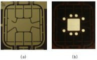
도 2는 도 1의 스마트 IC 칩 패키지의 정면 및 이면을 찍은 사진들이다
도 3은 본 발명의 일실시예에 따른 인쇄회로기판 제조 공정을 나타낸다.
도 4는 도 3의 인쇄회로기판을 포함하는 IC 칩 패키지의 단면을 나타낸 도면이다.
도 5는 본 발명의 다른 실시예에 따른 인쇄회로기판 제조 공정을 나타낸다.
142: 회로 패턴층 160: 와이어
150: IC 칩 170: 몰딩부
Claims (10)
- 폴리에틸렌 나프탈레이트(Polyethylene naphthalate, 이하 PET 라 함) 필름으로 형성된 절연층; 및
상기 절연층의 일 측면 상에 형성된 회로 패턴층을 포함하는 인쇄회로기판. - 종이(paper)로 형성된 절연층; 및
상기 절연층의 일 측면 상에 형성된 회로 패턴층을 포함하는 인쇄회로기판. - 청구항 1 또는 2에 있어서,
상기 회로 패턴층은 구리, 알루미늄, 또는 황동으로 형성되는 인쇄회로기판. - 청구항 1 또는 2에 있어서,
상기 절연층의 다른 면은 상기 절연층의 다른 면 상에 형성될 몰딩부의 접착력을 위해 거칠기를 갖도록 표면 처리되는 인쇄회로기판. - 청구항 1 또는 2에 있어서,
상기 절연층의 다른 면 상에 형성될 몰딩부의 접착력을 위해 상기 절연층의 다른 면 상에 형성되는 제1 접착층을 더 포함하는 인쇄회로기판. - 청구항 5에 있어서,
상기 절연층과 상기 회로패턴층 사이에 형성되는 제2 접착층을 더 포함하는 인쇄회로기판. - 청구항 1 또는 2의 인쇄회로기판;
상기 인쇄회로기판에 실장된 IC 칩;
상기 인쇄회로기판과 상기 IC 칩 사이에 본딩된 금속 와이어: 및
상기 IC 칩 및 상기 와이어 상에 형성된 몰딩부를 포함하는 IC 칩 패키지. - 청구항 7에 있어서,
상기 금속 와이어는 금 또는 알루미늄으로 이루어진 IC 칩 패키지. - 청구항 7에 있어서,
상기 몰딩부는 에폭시 수지로 이루어진 IC 칩 패키지. - 청구항 7에 있어서,
상기 몰딩부는 EMC(Epoxy Molding Compound) 몰드 방식, 댐앤필(Dam and Fill) 방식 또는 글로브탑(Grobtop) 방식을 이용하여 형성된 IC 칩 패키지.
Priority Applications (1)
| Application Number | Priority Date | Filing Date | Title |
|---|---|---|---|
| KR1020120069407A KR102007375B1 (ko) | 2012-06-27 | 2012-06-27 | 인쇄회로기판 및 이를 포함하는 ic 칩 패키지 |
Applications Claiming Priority (1)
| Application Number | Priority Date | Filing Date | Title |
|---|---|---|---|
| KR1020120069407A KR102007375B1 (ko) | 2012-06-27 | 2012-06-27 | 인쇄회로기판 및 이를 포함하는 ic 칩 패키지 |
Publications (2)
| Publication Number | Publication Date |
|---|---|
| KR20140001549A true KR20140001549A (ko) | 2014-01-07 |
| KR102007375B1 KR102007375B1 (ko) | 2019-08-06 |
Family
ID=50139055
Family Applications (1)
| Application Number | Title | Priority Date | Filing Date |
|---|---|---|---|
| KR1020120069407A Active KR102007375B1 (ko) | 2012-06-27 | 2012-06-27 | 인쇄회로기판 및 이를 포함하는 ic 칩 패키지 |
Country Status (1)
| Country | Link |
|---|---|
| KR (1) | KR102007375B1 (ko) |
Families Citing this family (1)
| Publication number | Priority date | Publication date | Assignee | Title |
|---|---|---|---|---|
| KR102719024B1 (ko) * | 2021-06-30 | 2024-10-17 | 주식회사 아젠컴 | 집적회로 카드, 집적회로 카드용 기판 구조체 및 그 제조 방법 |
Citations (4)
| Publication number | Priority date | Publication date | Assignee | Title |
|---|---|---|---|---|
| WO1999004367A1 (fr) * | 1997-07-18 | 1999-01-28 | Dai Nippon Printing Co., Ltd. | Module a circuit integre, carte a circuit integre, resine d'etancheite pour module a circuit integre, et procede de fabrication d'un module a circuit integre |
| JPH11288449A (ja) * | 1998-04-02 | 1999-10-19 | Toppan Printing Co Ltd | Icモジュール、icカードおよびicチップの樹脂封止方法 |
| JP2002103494A (ja) * | 2000-10-05 | 2002-04-09 | Matsushita Electric Ind Co Ltd | プリプレグとプリント配線基板およびその製造方法 |
| JP2006041162A (ja) * | 2004-07-27 | 2006-02-09 | Dainippon Printing Co Ltd | Icモジュールの製造方法、icカードとicカードの製造方法 |
-
2012
- 2012-06-27 KR KR1020120069407A patent/KR102007375B1/ko active Active
Patent Citations (4)
| Publication number | Priority date | Publication date | Assignee | Title |
|---|---|---|---|---|
| WO1999004367A1 (fr) * | 1997-07-18 | 1999-01-28 | Dai Nippon Printing Co., Ltd. | Module a circuit integre, carte a circuit integre, resine d'etancheite pour module a circuit integre, et procede de fabrication d'un module a circuit integre |
| JPH11288449A (ja) * | 1998-04-02 | 1999-10-19 | Toppan Printing Co Ltd | Icモジュール、icカードおよびicチップの樹脂封止方法 |
| JP2002103494A (ja) * | 2000-10-05 | 2002-04-09 | Matsushita Electric Ind Co Ltd | プリプレグとプリント配線基板およびその製造方法 |
| JP2006041162A (ja) * | 2004-07-27 | 2006-02-09 | Dainippon Printing Co Ltd | Icモジュールの製造方法、icカードとicカードの製造方法 |
Also Published As
| Publication number | Publication date |
|---|---|
| KR102007375B1 (ko) | 2019-08-06 |
Similar Documents
| Publication | Publication Date | Title |
|---|---|---|
| US8704101B2 (en) | Package carrier and manufacturing method thereof | |
| US9391044B2 (en) | Printed wiring board and method for manufacturing printed wiring board | |
| CN103650650B (zh) | 印刷电路板及其制造方法 | |
| JP2010287870A (ja) | プリント基板及びそれを含んだ半導体装置、並びにプリント基板の製造方法 | |
| KR101150036B1 (ko) | 전자소자 내장형 다층 연성인쇄회로기판 및 그 제조 방법 | |
| KR20080082365A (ko) | 금속 코어를 사용한 pcb, 그 제조방법 및 반도체 패키지제조방법 | |
| CN103281858A (zh) | 印刷电路板及其制造方法、倒装芯片封装件及其制造方法 | |
| KR20050087563A (ko) | 방열판이 장착된 인쇄회로기판과 이 회로기판을 이용한발광다이오드 패캐지 및 그 제조방법 | |
| KR101956119B1 (ko) | 스마트 ic용 인쇄회로기판 및 그 제조방법 | |
| KR102119760B1 (ko) | Ic 모듈용 인쇄회로기판 및 그 제조방법 | |
| US7607222B2 (en) | Method of manufacturing an electronic component package | |
| KR102007375B1 (ko) | 인쇄회로기판 및 이를 포함하는 ic 칩 패키지 | |
| KR20130134768A (ko) | 스마트 ic용 인쇄회로기판 및 그 제조 방법 | |
| KR101886340B1 (ko) | 스마트 ic모듈 및 그 제조방법 | |
| KR20130116657A (ko) | 칩 패키지 부재 제조 방법 및 칩 패키지 제조방법 | |
| KR101956103B1 (ko) | 인쇄회로기판 및 이를 포함하는 스마트 ic 모듈 | |
| KR20130135484A (ko) | 스마트 ic용 인쇄회로기판 및 그 제조방법 | |
| KR101510379B1 (ko) | 인쇄회로기판 어셈블리 | |
| KR101118878B1 (ko) | 회로 기판 및 그 제조 방법, 그리고 상기 회로 기판을 구비하는 반도체 패키지 및 그 제조 방법 | |
| KR101897015B1 (ko) | 칩 패키지 부재 제조 방법 및 칩 패키지 제조방법 | |
| KR101172168B1 (ko) | 방열회로기판 및 그의 제조 방법 | |
| KR20140039749A (ko) | Ic 칩 패키지용 기판 및 그 제조 방법 | |
| KR101814818B1 (ko) | 스마트 ic용 기판 | |
| US20160163624A1 (en) | Package structure | |
| KR20140078106A (ko) | 칩 패키지 및 그 제조방법 |
Legal Events
| Date | Code | Title | Description |
|---|---|---|---|
| PA0109 | Patent application |
St.27 status event code: A-0-1-A10-A12-nap-PA0109 |
|
| PG1501 | Laying open of application |
St.27 status event code: A-1-1-Q10-Q12-nap-PG1501 |
|
| PN2301 | Change of applicant |
St.27 status event code: A-3-3-R10-R13-asn-PN2301 St.27 status event code: A-3-3-R10-R11-asn-PN2301 |
|
| R17-X000 | Change to representative recorded |
St.27 status event code: A-3-3-R10-R17-oth-X000 |
|
| R18-X000 | Changes to party contact information recorded |
St.27 status event code: A-3-3-R10-R18-oth-X000 |
|
| A201 | Request for examination | ||
| PA0201 | Request for examination |
St.27 status event code: A-1-2-D10-D11-exm-PA0201 |
|
| R17-X000 | Change to representative recorded |
St.27 status event code: A-3-3-R10-R17-oth-X000 |
|
| D13-X000 | Search requested |
St.27 status event code: A-1-2-D10-D13-srh-X000 |
|
| R18-X000 | Changes to party contact information recorded |
St.27 status event code: A-3-3-R10-R18-oth-X000 |
|
| D14-X000 | Search report completed |
St.27 status event code: A-1-2-D10-D14-srh-X000 |
|
| E902 | Notification of reason for refusal | ||
| PE0902 | Notice of grounds for rejection |
St.27 status event code: A-1-2-D10-D21-exm-PE0902 |
|
| E13-X000 | Pre-grant limitation requested |
St.27 status event code: A-2-3-E10-E13-lim-X000 |
|
| P11-X000 | Amendment of application requested |
St.27 status event code: A-2-2-P10-P11-nap-X000 |
|
| P13-X000 | Application amended |
St.27 status event code: A-2-2-P10-P13-nap-X000 |
|
| E90F | Notification of reason for final refusal | ||
| PE0902 | Notice of grounds for rejection |
St.27 status event code: A-1-2-D10-D21-exm-PE0902 |
|
| P11-X000 | Amendment of application requested |
St.27 status event code: A-2-2-P10-P11-nap-X000 |
|
| P13-X000 | Application amended |
St.27 status event code: A-2-2-P10-P13-nap-X000 |
|
| E701 | Decision to grant or registration of patent right | ||
| PE0701 | Decision of registration |
St.27 status event code: A-1-2-D10-D22-exm-PE0701 |
|
| GRNT | Written decision to grant | ||
| PR0701 | Registration of establishment |
St.27 status event code: A-2-4-F10-F11-exm-PR0701 |
|
| PR1002 | Payment of registration fee |
St.27 status event code: A-2-2-U10-U11-oth-PR1002 Fee payment year number: 1 |
|
| PG1601 | Publication of registration |
St.27 status event code: A-4-4-Q10-Q13-nap-PG1601 |
|
| R18-X000 | Changes to party contact information recorded |
St.27 status event code: A-5-5-R10-R18-oth-X000 |
|
| PN2301 | Change of applicant |
St.27 status event code: A-5-5-R10-R13-asn-PN2301 St.27 status event code: A-5-5-R10-R11-asn-PN2301 |
|
| PR1001 | Payment of annual fee |
St.27 status event code: A-4-4-U10-U11-oth-PR1001 Fee payment year number: 4 |
|
| PR1001 | Payment of annual fee |
St.27 status event code: A-4-4-U10-U11-oth-PR1001 Fee payment year number: 5 |
|
| PR1001 | Payment of annual fee |
St.27 status event code: A-4-4-U10-U11-oth-PR1001 Fee payment year number: 6 |
|
| PR1001 | Payment of annual fee |
St.27 status event code: A-4-4-U10-U11-oth-PR1001 Fee payment year number: 7 |
|
| P22-X000 | Classification modified |
St.27 status event code: A-4-4-P10-P22-nap-X000 |