KR20140015331A - 잉크젯 기록용 도전성 수성 잉크 - Google Patents
잉크젯 기록용 도전성 수성 잉크 Download PDFInfo
- Publication number
- KR20140015331A KR20140015331A KR1020137021716A KR20137021716A KR20140015331A KR 20140015331 A KR20140015331 A KR 20140015331A KR 1020137021716 A KR1020137021716 A KR 1020137021716A KR 20137021716 A KR20137021716 A KR 20137021716A KR 20140015331 A KR20140015331 A KR 20140015331A
- Authority
- KR
- South Korea
- Prior art keywords
- inkjet recording
- aqueous ink
- polyhydric alcohol
- ink
- dispersion
- Prior art date
- Legal status (The legal status is an assumption and is not a legal conclusion. Google has not performed a legal analysis and makes no representation as to the accuracy of the status listed.)
- Granted
Links
Classifications
-
- H—ELECTRICITY
- H01—ELECTRIC ELEMENTS
- H01B—CABLES; CONDUCTORS; INSULATORS; SELECTION OF MATERIALS FOR THEIR CONDUCTIVE, INSULATING OR DIELECTRIC PROPERTIES
- H01B1/00—Conductors or conductive bodies characterised by the conductive materials; Selection of materials as conductors
- H01B1/20—Conductive material dispersed in non-conductive organic material
- H01B1/22—Conductive material dispersed in non-conductive organic material the conductive material comprising metals or alloys
-
- B—PERFORMING OPERATIONS; TRANSPORTING
- B05—SPRAYING OR ATOMISING IN GENERAL; APPLYING FLUENT MATERIALS TO SURFACES, IN GENERAL
- B05D—PROCESSES FOR APPLYING FLUENT MATERIALS TO SURFACES, IN GENERAL
- B05D5/00—Processes for applying liquids or other fluent materials to surfaces to obtain special surface effects, finishes or structures
- B05D5/12—Processes for applying liquids or other fluent materials to surfaces to obtain special surface effects, finishes or structures to obtain a coating with specific electrical properties
-
- C—CHEMISTRY; METALLURGY
- C09—DYES; PAINTS; POLISHES; NATURAL RESINS; ADHESIVES; COMPOSITIONS NOT OTHERWISE PROVIDED FOR; APPLICATIONS OF MATERIALS NOT OTHERWISE PROVIDED FOR
- C09D—COATING COMPOSITIONS, e.g. PAINTS, VARNISHES OR LACQUERS; FILLING PASTES; CHEMICAL PAINT OR INK REMOVERS; INKS; CORRECTING FLUIDS; WOODSTAINS; PASTES OR SOLIDS FOR COLOURING OR PRINTING; USE OF MATERIALS THEREFOR
- C09D11/00—Inks
- C09D11/30—Inkjet printing inks
-
- C—CHEMISTRY; METALLURGY
- C09—DYES; PAINTS; POLISHES; NATURAL RESINS; ADHESIVES; COMPOSITIONS NOT OTHERWISE PROVIDED FOR; APPLICATIONS OF MATERIALS NOT OTHERWISE PROVIDED FOR
- C09D—COATING COMPOSITIONS, e.g. PAINTS, VARNISHES OR LACQUERS; FILLING PASTES; CHEMICAL PAINT OR INK REMOVERS; INKS; CORRECTING FLUIDS; WOODSTAINS; PASTES OR SOLIDS FOR COLOURING OR PRINTING; USE OF MATERIALS THEREFOR
- C09D11/00—Inks
- C09D11/30—Inkjet printing inks
- C09D11/32—Inkjet printing inks characterised by colouring agents
- C09D11/322—Pigment inks
-
- C—CHEMISTRY; METALLURGY
- C09—DYES; PAINTS; POLISHES; NATURAL RESINS; ADHESIVES; COMPOSITIONS NOT OTHERWISE PROVIDED FOR; APPLICATIONS OF MATERIALS NOT OTHERWISE PROVIDED FOR
- C09D—COATING COMPOSITIONS, e.g. PAINTS, VARNISHES OR LACQUERS; FILLING PASTES; CHEMICAL PAINT OR INK REMOVERS; INKS; CORRECTING FLUIDS; WOODSTAINS; PASTES OR SOLIDS FOR COLOURING OR PRINTING; USE OF MATERIALS THEREFOR
- C09D11/00—Inks
- C09D11/30—Inkjet printing inks
- C09D11/38—Inkjet printing inks characterised by non-macromolecular additives other than solvents, pigments or dyes
-
- C—CHEMISTRY; METALLURGY
- C09—DYES; PAINTS; POLISHES; NATURAL RESINS; ADHESIVES; COMPOSITIONS NOT OTHERWISE PROVIDED FOR; APPLICATIONS OF MATERIALS NOT OTHERWISE PROVIDED FOR
- C09D—COATING COMPOSITIONS, e.g. PAINTS, VARNISHES OR LACQUERS; FILLING PASTES; CHEMICAL PAINT OR INK REMOVERS; INKS; CORRECTING FLUIDS; WOODSTAINS; PASTES OR SOLIDS FOR COLOURING OR PRINTING; USE OF MATERIALS THEREFOR
- C09D11/00—Inks
- C09D11/52—Electrically conductive inks
-
- H—ELECTRICITY
- H05—ELECTRIC TECHNIQUES NOT OTHERWISE PROVIDED FOR
- H05K—PRINTED CIRCUITS; CASINGS OR CONSTRUCTIONAL DETAILS OF ELECTRIC APPARATUS; MANUFACTURE OF ASSEMBLAGES OF ELECTRICAL COMPONENTS
- H05K3/00—Apparatus or processes for manufacturing printed circuits
- H05K3/10—Apparatus or processes for manufacturing printed circuits in which conductive material is applied to the insulating support in such a manner as to form the desired conductive pattern
- H05K3/12—Apparatus or processes for manufacturing printed circuits in which conductive material is applied to the insulating support in such a manner as to form the desired conductive pattern using thick film techniques, e.g. printing techniques to apply the conductive material or similar techniques for applying conductive paste or ink patterns
- H05K3/1241—Apparatus or processes for manufacturing printed circuits in which conductive material is applied to the insulating support in such a manner as to form the desired conductive pattern using thick film techniques, e.g. printing techniques to apply the conductive material or similar techniques for applying conductive paste or ink patterns by ink-jet printing or drawing by dispensing
- H05K3/125—Apparatus or processes for manufacturing printed circuits in which conductive material is applied to the insulating support in such a manner as to form the desired conductive pattern using thick film techniques, e.g. printing techniques to apply the conductive material or similar techniques for applying conductive paste or ink patterns by ink-jet printing or drawing by dispensing by ink-jet printing
Landscapes
- Chemical & Material Sciences (AREA)
- Engineering & Computer Science (AREA)
- Life Sciences & Earth Sciences (AREA)
- Materials Engineering (AREA)
- Wood Science & Technology (AREA)
- Organic Chemistry (AREA)
- Spectroscopy & Molecular Physics (AREA)
- Dispersion Chemistry (AREA)
- Physics & Mathematics (AREA)
- Manufacturing & Machinery (AREA)
- Microelectronics & Electronic Packaging (AREA)
- Inks, Pencil-Leads, Or Crayons (AREA)
- Conductive Materials (AREA)
- Manufacturing Of Printed Wiring (AREA)
- Ink Jet Recording Methods And Recording Media Thereof (AREA)
- Manufacturing Of Electric Cables (AREA)
- Ink Jet (AREA)
Abstract
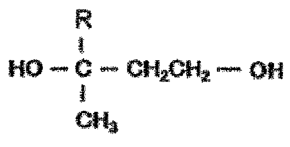
(상기 식 중, R은 수소 원자, 메틸기, 에틸기, n-프로필기로 이루어지는 군에서 선택되는 어느 하나의 저급 알킬기를 나타낸다)
Description

Claims (2)
- 금속 나노 입자(X)와, 다가 알코올(A)과, 물(B)을 함유하는 잉크젯 기록용 도전성 수성 잉크에 있어서, 다가 알코올(A)로서, 하기 일반식으로 표시되는 다가 알코올을 사용하는 것을 특징으로 하는 잉크젯 기록용 도전성 수성 잉크.
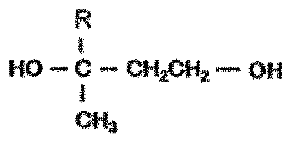
(상기 식 중, R은 수소 원자, 메틸기, 에틸기, n-프로필기로 이루어지는 군에서 선택되는 어느 하나의 저급 알킬기를 나타낸다) - 제1항에 있어서,
일반식으로 표시되는 다가 알코올이, 이소프렌글리콜 및/또는 1,3-부틸렌글리콜인 잉크젯 기록용 도전성 수성 잉크.
Applications Claiming Priority (3)
| Application Number | Priority Date | Filing Date | Title |
|---|---|---|---|
| JP2011050126 | 2011-03-08 | ||
| JPJP-P-2011-050126 | 2011-03-08 | ||
| PCT/JP2012/055524 WO2012121196A1 (ja) | 2011-03-08 | 2012-03-05 | インクジェット記録用導電性水性インク |
Publications (2)
| Publication Number | Publication Date |
|---|---|
| KR20140015331A true KR20140015331A (ko) | 2014-02-06 |
| KR101853695B1 KR101853695B1 (ko) | 2018-05-02 |
Family
ID=46798158
Family Applications (1)
| Application Number | Title | Priority Date | Filing Date |
|---|---|---|---|
| KR1020137021716A Expired - Fee Related KR101853695B1 (ko) | 2011-03-08 | 2012-03-05 | 잉크젯 기록용 도전성 수성 잉크 |
Country Status (7)
| Country | Link |
|---|---|
| US (1) | US9384868B2 (ko) |
| EP (1) | EP2684918B1 (ko) |
| JP (2) | JP5310957B2 (ko) |
| KR (1) | KR101853695B1 (ko) |
| CN (1) | CN103415580A (ko) |
| TW (1) | TWI540188B (ko) |
| WO (1) | WO2012121196A1 (ko) |
Families Citing this family (9)
| Publication number | Priority date | Publication date | Assignee | Title |
|---|---|---|---|---|
| WO2014052887A2 (en) * | 2012-09-27 | 2014-04-03 | Rhodia Operations | Process for making silver nanostructures and copolymer useful in such process |
| TWI574284B (zh) * | 2014-06-25 | 2017-03-11 | 柯尼卡美能達股份有限公司 | 附導電性圖案基材之製造方法 |
| CN108148471A (zh) * | 2016-12-05 | 2018-06-12 | 洛阳尖端技术研究院 | 一种导电油墨及其制备方法 |
| JP2018180168A (ja) * | 2017-04-07 | 2018-11-15 | ホヤ レンズ タイランド リミテッドHOYA Lens Thailand Ltd | 処理パターンが形成された光学部材の製造方法 |
| JP6530019B2 (ja) * | 2017-08-08 | 2019-06-12 | 田中貴金属工業株式会社 | 金属インク |
| JP7019996B2 (ja) * | 2017-08-23 | 2022-02-16 | コニカミノルタ株式会社 | 水系インクおよび画像形成方法 |
| CN112088193A (zh) * | 2018-05-08 | 2020-12-15 | 爱克发-格法特公司 | 导电油墨 |
| JPWO2022091883A1 (ko) * | 2020-10-27 | 2022-05-05 | ||
| CN115651448B (zh) * | 2021-07-07 | 2024-04-09 | 华南理工大学 | 一种具备n型导电的导电油墨及其制备与应用 |
Family Cites Families (19)
| Publication number | Priority date | Publication date | Assignee | Title |
|---|---|---|---|---|
| US5286415A (en) * | 1992-12-28 | 1994-02-15 | Advanced Products, Inc. | Water-based polymer thick film conductive ink |
| CN101036199A (zh) * | 2004-10-08 | 2007-09-12 | 三井金属矿业株式会社 | 导电性油墨 |
| JP4799881B2 (ja) * | 2004-12-27 | 2011-10-26 | 三井金属鉱業株式会社 | 導電性インク |
| JP2007146117A (ja) * | 2005-11-04 | 2007-06-14 | Mitsui Mining & Smelting Co Ltd | ニッケルインク及びそのニッケルインクで形成した導体膜 |
| US8277693B2 (en) * | 2006-07-28 | 2012-10-02 | Furukawa Electric Co., Ltd. | Method for producing fine particle dispersion and fine particle dispersion |
| DE102007037079A1 (de) * | 2006-10-25 | 2008-04-30 | Bayer Materialscience Ag | Silberhaltige wässrige Formulierung und ihre Verwendung zur Herstellung von elektrisch leitenden oder spiegelnden Beschichtungen |
| JP2008184567A (ja) * | 2007-01-31 | 2008-08-14 | Ricoh Co Ltd | 記録用インク、並びにインクカートリッジ、インクジェット記録方法、及びインクジェット記録装置 |
| KR20080088712A (ko) * | 2007-03-30 | 2008-10-06 | 삼성전자주식회사 | 전도성 잉크 조성물 및 이를 이용한 전도성 패턴의 형성방법 |
| EP2147733A4 (en) | 2007-05-16 | 2012-12-12 | Dainippon Ink & Chemicals | Method for production of silver-containing nano-structure, and silver-containing nano-structure |
| JP2009091383A (ja) | 2007-10-03 | 2009-04-30 | Seiko Epson Corp | 導体パターン形成用インク、導体パターンおよび配線基板 |
| JP4867905B2 (ja) * | 2007-12-11 | 2012-02-01 | セイコーエプソン株式会社 | 導体パターン形成用インク、導体パターン、および配線基板 |
| CN101519552B (zh) * | 2008-02-29 | 2011-08-24 | 中国科学院化学研究所 | 含贵金属纳米颗粒的喷墨水溶性墨水的制备方法 |
| US8506849B2 (en) * | 2008-03-05 | 2013-08-13 | Applied Nanotech Holdings, Inc. | Additives and modifiers for solvent- and water-based metallic conductive inks |
| JP5117420B2 (ja) * | 2008-03-27 | 2013-01-16 | 古河電気工業株式会社 | 銅微粒子分散水溶液の製造方法及び銅微粒子分散水溶液の保管方法 |
| JP2010047807A (ja) | 2008-08-22 | 2010-03-04 | Seiko Epson Corp | 複合化金属薄膜粒子、複合化金属薄膜粒子分散液、導電回路製造用インク、導電回路の製造方法および導電回路 |
| JP5201407B2 (ja) | 2008-09-24 | 2013-06-05 | Dic株式会社 | 導電性インクジェットインク |
| JP5661273B2 (ja) * | 2008-11-26 | 2015-01-28 | 三ツ星ベルト株式会社 | 金属コロイド粒子及びそのペースト並びにその製造方法 |
| JP5399100B2 (ja) * | 2009-03-04 | 2014-01-29 | 三ツ星ベルト株式会社 | 金属コロイド粒子凝集体及びその製造方法 |
| CN101805538B (zh) * | 2010-04-08 | 2014-05-07 | 中国科学院宁波材料技术与工程研究所 | 可低温烧结的导电墨水 |
-
2012
- 2012-03-05 CN CN2012800120159A patent/CN103415580A/zh active Pending
- 2012-03-05 KR KR1020137021716A patent/KR101853695B1/ko not_active Expired - Fee Related
- 2012-03-05 US US14/003,520 patent/US9384868B2/en not_active Expired - Fee Related
- 2012-03-05 JP JP2012537254A patent/JP5310957B2/ja active Active
- 2012-03-05 EP EP12754756.0A patent/EP2684918B1/en not_active Not-in-force
- 2012-03-05 WO PCT/JP2012/055524 patent/WO2012121196A1/ja not_active Ceased
- 2012-03-08 TW TW101107809A patent/TWI540188B/zh not_active IP Right Cessation
-
2013
- 2013-05-10 JP JP2013099780A patent/JP2013225515A/ja active Pending
Also Published As
| Publication number | Publication date |
|---|---|
| JPWO2012121196A1 (ja) | 2014-07-17 |
| CN103415580A (zh) | 2013-11-27 |
| KR101853695B1 (ko) | 2018-05-02 |
| EP2684918A1 (en) | 2014-01-15 |
| WO2012121196A1 (ja) | 2012-09-13 |
| TWI540188B (zh) | 2016-07-01 |
| US20140134327A1 (en) | 2014-05-15 |
| EP2684918A4 (en) | 2015-04-29 |
| JP5310957B2 (ja) | 2013-10-09 |
| EP2684918B1 (en) | 2018-09-12 |
| TW201245348A (en) | 2012-11-16 |
| JP2013225515A (ja) | 2013-10-31 |
| US9384868B2 (en) | 2016-07-05 |
Similar Documents
| Publication | Publication Date | Title |
|---|---|---|
| JP5310957B2 (ja) | インクジェット記録用導電性水性インク | |
| JP6083623B2 (ja) | 銀ナノ粒子及び銀ナノ粒子インク | |
| KR101248447B1 (ko) | 스크린 인쇄용 도전성 페이스트 | |
| TWI583753B (zh) | 導電性印墨組成物 | |
| JP2009275227A (ja) | 銀ナノ粒子含有印刷可能組成物、該組成物を用いた導電性被膜の製造方法、および該方法により製造された被膜 | |
| US20130264104A1 (en) | Conductive metal ink composition, and method for forming a conductive pattern | |
| US10774231B2 (en) | Composition for sintering, method for producing silver nanoparticles, circuit board, and method for manufacturing circuit board | |
| DE102016225051A1 (de) | Zwischenschichtzusammensetzung für elektronisches drucken | |
| JPWO2016125355A1 (ja) | 導電性の微小粒子 | |
| JP6404261B2 (ja) | 銀粉 | |
| JP2014067677A (ja) | 導電ペースト、プリント配線基板 | |
| Shabbir et al. | Introduction to smart multifunctional metal nano-inks | |
| KR102959075B1 (ko) | 인쇄 제품, 그를 위한 제조 방법, 및 그의 용도 | |
| EP3231607B1 (en) | Interlayer composition and devices made therefrom | |
| KR100772440B1 (ko) | 미세배선 형성방법 | |
| CN109996386A (zh) | 一种实现纳米银颗粒墨水室温烧结的预涂层及其制备方法 | |
| JP2020181710A (ja) | 塗布剤、印刷物、及び印刷物の製造方法 | |
| CN110128879A (zh) | 一种用于喷墨打印的纳米钨墨水及其制备方法 | |
| KR20190073217A (ko) | 잉크젯 프린팅용 구리나노잉크 |
Legal Events
| Date | Code | Title | Description |
|---|---|---|---|
| PA0105 | International application |
St.27 status event code: A-0-1-A10-A15-nap-PA0105 |
|
| P11-X000 | Amendment of application requested |
St.27 status event code: A-2-2-P10-P11-nap-X000 |
|
| P13-X000 | Application amended |
St.27 status event code: A-2-2-P10-P13-nap-X000 |
|
| PG1501 | Laying open of application |
St.27 status event code: A-1-1-Q10-Q12-nap-PG1501 |
|
| A201 | Request for examination | ||
| P11-X000 | Amendment of application requested |
St.27 status event code: A-2-2-P10-P11-nap-X000 |
|
| P13-X000 | Application amended |
St.27 status event code: A-2-2-P10-P13-nap-X000 |
|
| PA0201 | Request for examination |
St.27 status event code: A-1-2-D10-D11-exm-PA0201 |
|
| E902 | Notification of reason for refusal | ||
| PE0902 | Notice of grounds for rejection |
St.27 status event code: A-1-2-D10-D21-exm-PE0902 |
|
| T11-X000 | Administrative time limit extension requested |
St.27 status event code: U-3-3-T10-T11-oth-X000 |
|
| E13-X000 | Pre-grant limitation requested |
St.27 status event code: A-2-3-E10-E13-lim-X000 |
|
| P11-X000 | Amendment of application requested |
St.27 status event code: A-2-2-P10-P11-nap-X000 |
|
| P13-X000 | Application amended |
St.27 status event code: A-2-2-P10-P13-nap-X000 |
|
| E701 | Decision to grant or registration of patent right | ||
| PE0701 | Decision of registration |
St.27 status event code: A-1-2-D10-D22-exm-PE0701 |
|
| GRNT | Written decision to grant | ||
| PR0701 | Registration of establishment |
St.27 status event code: A-2-4-F10-F11-exm-PR0701 |
|
| PR1002 | Payment of registration fee |
St.27 status event code: A-2-2-U10-U12-oth-PR1002 Fee payment year number: 1 |
|
| PG1601 | Publication of registration |
St.27 status event code: A-4-4-Q10-Q13-nap-PG1601 |
|
| PC1903 | Unpaid annual fee |
St.27 status event code: A-4-4-U10-U13-oth-PC1903 Not in force date: 20210426 Payment event data comment text: Termination Category : DEFAULT_OF_REGISTRATION_FEE |
|
| PC1903 | Unpaid annual fee |
St.27 status event code: N-4-6-H10-H13-oth-PC1903 Ip right cessation event data comment text: Termination Category : DEFAULT_OF_REGISTRATION_FEE Not in force date: 20210426 |