KR20140020190A - 웨이퍼 레벨의 발광 다이오드 어레이 및 그의 제조방법 - Google Patents
웨이퍼 레벨의 발광 다이오드 어레이 및 그의 제조방법 Download PDFInfo
- Publication number
- KR20140020190A KR20140020190A KR1020130088709A KR20130088709A KR20140020190A KR 20140020190 A KR20140020190 A KR 20140020190A KR 1020130088709 A KR1020130088709 A KR 1020130088709A KR 20130088709 A KR20130088709 A KR 20130088709A KR 20140020190 A KR20140020190 A KR 20140020190A
- Authority
- KR
- South Korea
- Prior art keywords
- light emitting
- semiconductor layer
- emitting diode
- electrodes
- interlayer insulating
- Prior art date
- Legal status (The legal status is an assumption and is not a legal conclusion. Google has not performed a legal analysis and makes no representation as to the accuracy of the status listed.)
- Granted
Links
- 238000000034 method Methods 0.000 title claims description 44
- 239000004065 semiconductor Substances 0.000 claims abstract description 153
- 239000000758 substrate Substances 0.000 claims abstract description 44
- 238000004519 manufacturing process Methods 0.000 claims abstract description 12
- 239000000463 material Substances 0.000 claims abstract description 8
- 239000010410 layer Substances 0.000 claims description 229
- 239000011229 interlayer Substances 0.000 claims description 65
- 229910052804 chromium Inorganic materials 0.000 claims description 4
- 229910052759 nickel Inorganic materials 0.000 claims description 4
- 229910052703 rhodium Inorganic materials 0.000 claims description 4
- 229910052782 aluminium Inorganic materials 0.000 claims description 3
- 238000005520 cutting process Methods 0.000 claims description 2
- 239000007769 metal material Substances 0.000 claims description 2
- 229910052719 titanium Inorganic materials 0.000 claims description 2
- 239000010408 film Substances 0.000 description 20
- 238000005530 etching Methods 0.000 description 14
- 239000002184 metal Substances 0.000 description 10
- 229910052751 metal Inorganic materials 0.000 description 10
- 229920002120 photoresistant polymer Polymers 0.000 description 7
- 238000010586 diagram Methods 0.000 description 6
- 230000015572 biosynthetic process Effects 0.000 description 5
- 238000006243 chemical reaction Methods 0.000 description 3
- 230000006866 deterioration Effects 0.000 description 3
- 230000020169 heat generation Effects 0.000 description 3
- 238000000465 moulding Methods 0.000 description 3
- 238000012858 packaging process Methods 0.000 description 3
- 238000000059 patterning Methods 0.000 description 3
- 238000000926 separation method Methods 0.000 description 3
- 230000004888 barrier function Effects 0.000 description 2
- 229910052697 platinum Inorganic materials 0.000 description 2
- 229910052709 silver Inorganic materials 0.000 description 2
- 229910002601 GaN Inorganic materials 0.000 description 1
- 206010039740 Screaming Diseases 0.000 description 1
- 229910004298 SiO 2 Inorganic materials 0.000 description 1
- 239000002131 composite material Substances 0.000 description 1
- 238000005336 cracking Methods 0.000 description 1
- 239000013078 crystal Substances 0.000 description 1
- 238000009826 distribution Methods 0.000 description 1
- 239000012467 final product Substances 0.000 description 1
- 238000010438 heat treatment Methods 0.000 description 1
- 230000001939 inductive effect Effects 0.000 description 1
- 239000011810 insulating material Substances 0.000 description 1
- 238000009413 insulation Methods 0.000 description 1
- 239000012212 insulator Substances 0.000 description 1
- 238000002955 isolation Methods 0.000 description 1
- 238000004806 packaging method and process Methods 0.000 description 1
- 229910052594 sapphire Inorganic materials 0.000 description 1
- 239000010980 sapphire Substances 0.000 description 1
- HBMJWWWQQXIZIP-UHFFFAOYSA-N silicon carbide Chemical compound [Si+]#[C-] HBMJWWWQQXIZIP-UHFFFAOYSA-N 0.000 description 1
- 229910010271 silicon carbide Inorganic materials 0.000 description 1
- 239000002356 single layer Substances 0.000 description 1
- 238000002207 thermal evaporation Methods 0.000 description 1
- 239000010409 thin film Substances 0.000 description 1
- 238000002834 transmittance Methods 0.000 description 1
Images













Classifications
-
- H—ELECTRICITY
- H10—SEMICONDUCTOR DEVICES; ELECTRIC SOLID-STATE DEVICES NOT OTHERWISE PROVIDED FOR
- H10H—INORGANIC LIGHT-EMITTING SEMICONDUCTOR DEVICES HAVING POTENTIAL BARRIERS
- H10H29/00—Integrated devices, or assemblies of multiple devices, comprising at least one light-emitting semiconductor element covered by group H10H20/00
- H10H29/10—Integrated devices comprising at least one light-emitting semiconductor component covered by group H10H20/00
- H10H29/14—Integrated devices comprising at least one light-emitting semiconductor component covered by group H10H20/00 comprising multiple light-emitting semiconductor components
- H10H29/142—Two-dimensional arrangements, e.g. asymmetric LED layout
-
- H—ELECTRICITY
- H10—SEMICONDUCTOR DEVICES; ELECTRIC SOLID-STATE DEVICES NOT OTHERWISE PROVIDED FOR
- H10H—INORGANIC LIGHT-EMITTING SEMICONDUCTOR DEVICES HAVING POTENTIAL BARRIERS
- H10H20/00—Individual inorganic light-emitting semiconductor devices having potential barriers, e.g. light-emitting diodes [LED]
- H10H20/80—Constructional details
- H10H20/83—Electrodes
- H10H20/831—Electrodes characterised by their shape
-
- H—ELECTRICITY
- H10—SEMICONDUCTOR DEVICES; ELECTRIC SOLID-STATE DEVICES NOT OTHERWISE PROVIDED FOR
- H10H—INORGANIC LIGHT-EMITTING SEMICONDUCTOR DEVICES HAVING POTENTIAL BARRIERS
- H10H20/00—Individual inorganic light-emitting semiconductor devices having potential barriers, e.g. light-emitting diodes [LED]
- H10H20/80—Constructional details
- H10H20/85—Packages
- H10H20/857—Interconnections, e.g. lead-frames, bond wires or solder balls
Landscapes
- Led Devices (AREA)
- Led Device Packages (AREA)
Abstract
Description
도 3 및 도 4는 도 1의 제2 반도체층 상에 하부 전극들이 형성된 것을 도시한 평면도 및 단면도이다.
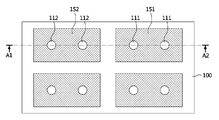
도 5는 도 3의 구조물에 대해 셀 영역들이 분리된 상태를 도시한 평면도이다.
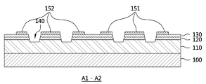
도 6은 도 5의 평면도를 A1-A2 라인을 따라 절단한 단면도이다.
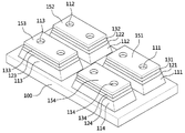
도 7은 도 5의 평면도의 사시도이다.
도 8은 도 5 내지 도 7의 구조물 전면에 제1 층간 절연막을 형성하고, 각각의 셀 영역에서 제1 반도체층 및 하부전극의 일부를 노출한 평면도이다.
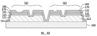
도 9 내지 도 12는 도 8의 평면도를 특정의 라인을 따라 절개한 단면도들이다.
도 13은 도 8 내지 도 12에 개시된 구조물 상에 상부 전극들을 형성한 평면도이다.
도 14 내지 도 17은 도 13의 평면도를 특정의 라인을 따라 절개한 단면도들이다.
도 18은 도 13의 평면도를 도시한 사시도이다.
도 19는 본 발명의 실시예에 따라 도 13 내지 도 18의 구조물을 모델링한 등가 회로도이다.
도 20은 도 13의 평면도에서 구조물의 전면에 제2 층간 절연막을 도포하고, 제1 셀 영역의 제1 하부 전극의 일부를 노출하고, 제4 셀 영역의 제4 하부 전극의 일부를 노출한 평면도이다.
도 21 내지 도 24는 도 20의 평면도를 특정 라인을 따라 절개한 단면도들이다.
도 25는 도 20의 구조물에 제1 패드 및 제2 패드를 형성한 평면도이다.
도 26 내지 도 29는 도 25의 평면도를 특정 라인을 따라 절개한 단면도들이다.
도 30은 도 25의 평면도를 C2-C3 라인을 따라 절개한 사시도이다.
도 31은 본 발명의 일 실시예에 따라, 10개의 발광 다이오드들을 직렬로 연결하도록 모델링한 회로도이다.
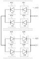
도 32는 본 발명의 일 실시예에 따라, 직/병렬 형태로 발광 다이오드들이 어레이를 구성한 것을 모델링한 회로도이다.
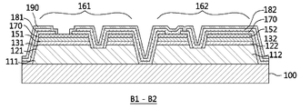
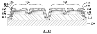
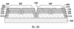
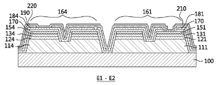
121, 122, 123, 124 : 활성층 131, 132, 133, 134 : 제2 반도체층
140 : 비아홀 151 : 제1 하부 전극
152 : 제2 하부 전극 153 : 제3 하부 전극
154 : 제4 하부 전극 161 : 제1 셀 영역
162 : 제2 셀 영역 163 : 제3 셀 영역
164 : 제4 셀 영역 170 : 제1 층간 절연막
181 : 제1 상부 전극 182 : 제2 상부 전극
183 : 제3 상부 전극 184 : 제4 상부 전극
190 : 제2 층간 절연막 210 : 제1 패드
220 : 제2 패드
Claims (20)
- 성장 기판;
상기 기판 상에 정렬되며, 각각 제1 반도체층, 활성층 및 제2 반도체층을 포함하는 복수개의 발광 다이오드들; 및
상기 복수개의 발광 다이오드들 상에 정렬되며, 서로 동일한 재료로 형성되고, 각각 대응하는 발광 다이오드의 제1 반도체층에 전기적으로 접속하는 복수개의 상부 전극들을 포함하고,
상기 상부 전극들 중 하나 이상은 인접한 발광 다이오드의 제2 반도체층에 전기적으로 접속하며, 상기 상부 전극들 중 다른 하나는 인접한 발광 다이오드의 제2 반도체층으로부터 절연된 발광 다이오드 어레이. - 청구항 1에 있어서,
상기 상부 전극들은 제1 반도체층에 오믹 콘택하는 오믹 콘택층을 포함하는 발광 다이오드 어레이. - 청구항 2에 있어서,
상기 오믹 콘택층은 Cr, Ni, Ti, Rh 및 Al으로 이루어진 군에서 선택된 어느 하나의 금속 물질을 포함하는 발광 다이오드 어레이. - 청구항 1에 있어서,
상기 오믹 콘택층은 ITO를 포함하는 발광 다이오드 어레이. - 청구항 2에 있어서,
상기 상부 전극들은 상기 오믹 콘택층 상에 위치하는 반사층을 더 포함하는 발광 다이오드 어레이. - 청구항 1에 있어서,
상기 발광 다이오드들과 상기 상부 전극들 사이에 정렬된 제1 층간 절연막을 더 포함하고,
상기 상부 전극들을 상기 제1 층간 절연막에 의해 상기 발광 다이오드들의 측면으로부터 절연되는 발광 다이오드 어레이. - 청구항 6에 있어서,
각 발광 다이오드의 제2 반도체층 상에 정렬된 하부 전극들을 더 포함하되,
상기 제1 층간 절연막은 각 발광 다이오드 상의 하부 전극의 일부를 노출시키고,
상기 인접한 발광 다이오드의 제2 반도체층에 전기적으로 접속하는 상부 전극(들)은 상기 제1 층간 절연막을 통해 상기 노출된 하부 전극에 접속하는 발광 다이오드 어레이. - 청구항 7에 있어서,
상기 하부 전극들은 각각 반사층을 포함하는 발광 다이오드 어레이. - 청구항 7에 있어서,
상기 상부 전극들을 덮는 제2 층간 절연막을 더 포함하되,
상기 제2 층간 절연막은 상기 하부 전극들 중 하나와 상기 인접한 발광 다이오드의 제2 반도체층으로부터 절연된 상부 전극을 노출시키는 발광 다이오드 어레이. - 청구항 9에 있어서,
상기 발광 다이오드들은 상기 상부 전극들에 의해 직렬 연결되고,
상기 제2 층간 절연막은 상기 직렬 연결된 발광 다이오드들 중 양측 단부의 발광 다이오드들에 대응하는 하부 전극 및 상부 전극을 노출시키는 발광 다이오드 어레이. - 청구항 9에 있어서,
상기 제2 층간 절연막 상에 위치하는 제1 패드 및 제2 패드를 더 포함하되,
상기 제1 패드는 상기 제2 층간 절연막을 통해 노출된 하부 전극에 접속되고, 상기 제2 패드는 상기 제2 층간 절연막을 통해 노출된 상부 전극에 접속하는 발광 다이오드 어레이. - 청구항 1에 있어서,
상기 발광 다이오드들은 각각 제2 반도체층 및 활성층을 통해 상기 제1 반도체층을 노출하는 비아홀을 갖고,
상기 상부 전극들은 각각 상기 비아홀을 통해 대응하는 발광 다이오드의 제1 반도체층에 접속하는 발광 다이오드 어레이. - 청구항 1에 있어서,
상기 상부 전극은 상기 발광 다이오드 어레이의 전체 면적의 30% 이상 및 100% 미만의 면적을 점유하는 발광 다이오드 어레이. - 청구항 1에 있어서,
상기 상부 전극은 너비와 폭의 비가 1:3 내지 3:1의 범위 내에 있는 플레이트 또는 시트 형상을 갖는 발광 다이오드 어레이. - 청구항 1에 있어서,
상기 상부 전극들 중 적어도 하나는 대응하는 발광 다이오드의 너비 또는 폭에 비해 더 큰 너비 또는 폭을 갖는 발광 다이오드 어레이. - 성장 기판 상에 각각 제1 반도체층, 활성층 및 제2 반도체층을 포함하는 복수의 발광 다이오드들을 형성하되, 상기 발광 다이오드들은 각각 상기 제2 반도체층 및 활성층이 제거되어 노출된 제1 반도체층을 갖고,
상기 발광 다이오드들을 덮는 제1 층간 절연막을 형성하되, 상기 제1 층간 절연막은 상기 노출된 제1 반도체층들을 노출함과 아울러 각 발광 다이오드의 제2 반도체층 상부에 위치하는 개구부들을 갖고,
상기 제1 층간 절연막 상에 동일 재료로 복수의 상부 전극들을 형성하는 것을 포함하되,
상기 상부 전극들은 각각 대응하는 발광 다이오드의 제1 반도체층에 접속하고,
상기 상부 전극들 중 하나 이상은 상기 제1 층간 절연막의 개구부를 통해 인접한 발광 다이오드의 제2 반도체층에 전기적으로 접속하며, 상기 상부 전극들 중 다른 하나는 인접한 발광 다이오드의 제2 반도체층으로부터 절연된 발광 다이오드 어레이 제조 방법. - 청구항 16에 있어서,
상기 제1 층간 절연막을 형성하기 전에 각 발광 다이오드의 제2 반도체층 상에 하부 전극들을 형성하는 것을 더 포함하는 발광 다이오드 어레이 제조 방법. - 청구항 17에 있어서,
상기 상부 전극 상에 제2 층간 절연막을 형성하는 것을 더 포함하되,
상기 제2 층간 절연막은 상기 하부 전극들 중 하나와 상기 인접한 발광 다이오드의 제2 반도체층으로부터 절연된 다른 하나의 상부 전극을 노출하는 발광 다이오드 어레이 제조 방법. - 청구항 18에 있어서,
상기 제2 층간 절연막 상에 제1 패드 및 제2 패드를 형성하는 것을 더 포함하되,
상기 제1 패드는 상기 하부 전극에 접속하고, 상기 제2 패드는 상기 상부 전극에 접속하는 발광 다이오드 어레이 제조 방법. - 청구항 16에 있어서,
상기 성장 기판을 개별 단위로 절단하는 것을 더 포함하되,
상기 상부 전극은 절단된 개별 단위의 발광 다이오드 어레이 면적의 30% 이상 100% 미만의 면적을 점유하는 발광 다이오드 어레이 제조 방법.
Priority Applications (12)
| Application Number | Priority Date | Filing Date | Title |
|---|---|---|---|
| US14/420,175 US9318530B2 (en) | 2012-08-07 | 2013-08-06 | Wafer level light-emitting diode array and method for manufacturing same |
| IN390KON2015 IN2015KN00390A (ko) | 2012-08-07 | 2013-08-06 | |
| PCT/KR2013/007091 WO2014025195A1 (ko) | 2012-08-07 | 2013-08-06 | 웨이퍼 레벨의 발광 다이오드 어레이 및 그의 제조방법 |
| CN201380042047.8A CN104521012B (zh) | 2012-08-07 | 2013-08-06 | 晶圆级发光二极管阵列及其制造方法 |
| CN201810244405.8A CN108461515A (zh) | 2012-08-07 | 2013-08-06 | 晶圆级发光二极管阵列 |
| DE112013003931.1T DE112013003931T5 (de) | 2012-08-07 | 2013-08-06 | Leuchtdiodenarray auf Wafer-Ebene und Verfahren zu dessen Herstellung |
| DE202013012471.7U DE202013012471U1 (de) | 2012-08-07 | 2013-08-06 | Leuchtdiodenarray auf Wafer-Ebene |
| TW102128317A TWI599017B (zh) | 2012-08-07 | 2013-08-07 | 晶圓等級之發光二極體陣列及其製造方法 |
| US15/081,134 US10388690B2 (en) | 2012-08-07 | 2016-03-25 | Wafer level light-emitting diode array |
| US15/835,326 US10804316B2 (en) | 2012-08-07 | 2017-12-07 | Wafer level light-emitting diode array |
| US16/858,560 US11139338B2 (en) | 2012-08-07 | 2020-04-24 | Wafer level light-emitting diode array |
| US17/492,729 US11587972B2 (en) | 2012-08-07 | 2021-10-04 | Wafer level light-emitting diode array |
Applications Claiming Priority (2)
| Application Number | Priority Date | Filing Date | Title |
|---|---|---|---|
| KR1020120086329 | 2012-08-07 | ||
| KR20120086329 | 2012-08-07 |
Related Child Applications (2)
| Application Number | Title | Priority Date | Filing Date |
|---|---|---|---|
| KR1020160133589A Division KR101798134B1 (ko) | 2016-10-14 | 2016-10-14 | 웨이퍼 레벨의 발광 다이오드 어레이 및 그의 제조방법 |
| KR1020180096788A Division KR101949718B1 (ko) | 2012-08-07 | 2018-08-20 | 웨이퍼 레벨의 발광 다이오드 어레이 |
Publications (2)
| Publication Number | Publication Date |
|---|---|
| KR20140020190A true KR20140020190A (ko) | 2014-02-18 |
| KR101892213B1 KR101892213B1 (ko) | 2018-08-28 |
Family
ID=50267340
Family Applications (2)
| Application Number | Title | Priority Date | Filing Date |
|---|---|---|---|
| KR1020130088709A Active KR101892213B1 (ko) | 2012-08-07 | 2013-07-26 | 웨이퍼 레벨의 발광 다이오드 어레이 및 그의 제조방법 |
| KR1020180096788A Active KR101949718B1 (ko) | 2012-08-07 | 2018-08-20 | 웨이퍼 레벨의 발광 다이오드 어레이 |
Family Applications After (1)
| Application Number | Title | Priority Date | Filing Date |
|---|---|---|---|
| KR1020180096788A Active KR101949718B1 (ko) | 2012-08-07 | 2018-08-20 | 웨이퍼 레벨의 발광 다이오드 어레이 |
Country Status (1)
| Country | Link |
|---|---|
| KR (2) | KR101892213B1 (ko) |
Cited By (4)
| Publication number | Priority date | Publication date | Assignee | Title |
|---|---|---|---|---|
| KR20160085605A (ko) * | 2015-01-08 | 2016-07-18 | 엘지이노텍 주식회사 | 발광 소자 패키지 |
| WO2016148424A1 (ko) * | 2015-03-16 | 2016-09-22 | 서울바이오시스 주식회사 | 금속 벌크를 포함하는 발광 소자 |
| KR20160139181A (ko) * | 2015-05-27 | 2016-12-07 | 서울바이오시스 주식회사 | 발광소자 |
| CN110690249A (zh) * | 2015-02-13 | 2020-01-14 | 首尔伟傲世有限公司 | 发光元件 |
Families Citing this family (1)
| Publication number | Priority date | Publication date | Assignee | Title |
|---|---|---|---|---|
| EP4586321A1 (en) * | 2022-09-06 | 2025-07-16 | Seoul Semiconductor Co., Ltd. | Light-emitting device |
Citations (6)
| Publication number | Priority date | Publication date | Assignee | Title |
|---|---|---|---|---|
| US6573537B1 (en) | 1999-12-22 | 2003-06-03 | Lumileds Lighting, U.S., Llc | Highly reflective ohmic contacts to III-nitride flip-chip LEDs |
| KR20070035745A (ko) | 2005-09-28 | 2007-04-02 | 서울옵토디바이스주식회사 | 다수의 셀이 결합된 발광 소자 및 이의 제조 방법 |
| KR20080002161A (ko) | 2006-06-30 | 2008-01-04 | 서울옵토디바이스주식회사 | 확장된 금속 반사층을 갖는 플립 본딩형 발광다이오드 및그 제조방법 |
| KR20090053435A (ko) * | 2007-11-23 | 2009-05-27 | 삼성전기주식회사 | 모놀리식 발광다이오드 어레이 및 그 제조방법 |
| KR20100016631A (ko) * | 2007-04-26 | 2010-02-12 | 오스람 옵토 세미컨덕터스 게엠베하 | 광전 소자,및 복수 개의 광전 소자들의 제조 방법 |
| KR20100076083A (ko) * | 2008-12-17 | 2010-07-06 | 서울반도체 주식회사 | 복수개의 발광셀들을 갖는 발광 다이오드 및 그것을 제조하는 방법 |
Family Cites Families (2)
| Publication number | Priority date | Publication date | Assignee | Title |
|---|---|---|---|---|
| JP4160881B2 (ja) * | 2003-08-28 | 2008-10-08 | 松下電器産業株式会社 | 半導体発光装置、発光モジュール、照明装置、および半導体発光装置の製造方法 |
| WO2005022654A2 (en) * | 2003-08-28 | 2005-03-10 | Matsushita Electric Industrial Co.,Ltd. | Semiconductor light emitting device, light emitting module, lighting apparatus, display element and manufacturing method of semiconductor light emitting device |
-
2013
- 2013-07-26 KR KR1020130088709A patent/KR101892213B1/ko active Active
-
2018
- 2018-08-20 KR KR1020180096788A patent/KR101949718B1/ko active Active
Patent Citations (6)
| Publication number | Priority date | Publication date | Assignee | Title |
|---|---|---|---|---|
| US6573537B1 (en) | 1999-12-22 | 2003-06-03 | Lumileds Lighting, U.S., Llc | Highly reflective ohmic contacts to III-nitride flip-chip LEDs |
| KR20070035745A (ko) | 2005-09-28 | 2007-04-02 | 서울옵토디바이스주식회사 | 다수의 셀이 결합된 발광 소자 및 이의 제조 방법 |
| KR20080002161A (ko) | 2006-06-30 | 2008-01-04 | 서울옵토디바이스주식회사 | 확장된 금속 반사층을 갖는 플립 본딩형 발광다이오드 및그 제조방법 |
| KR20100016631A (ko) * | 2007-04-26 | 2010-02-12 | 오스람 옵토 세미컨덕터스 게엠베하 | 광전 소자,및 복수 개의 광전 소자들의 제조 방법 |
| KR20090053435A (ko) * | 2007-11-23 | 2009-05-27 | 삼성전기주식회사 | 모놀리식 발광다이오드 어레이 및 그 제조방법 |
| KR20100076083A (ko) * | 2008-12-17 | 2010-07-06 | 서울반도체 주식회사 | 복수개의 발광셀들을 갖는 발광 다이오드 및 그것을 제조하는 방법 |
Cited By (8)
| Publication number | Priority date | Publication date | Assignee | Title |
|---|---|---|---|---|
| KR20160085605A (ko) * | 2015-01-08 | 2016-07-18 | 엘지이노텍 주식회사 | 발광 소자 패키지 |
| CN110690249A (zh) * | 2015-02-13 | 2020-01-14 | 首尔伟傲世有限公司 | 发光元件 |
| US11282892B2 (en) | 2015-02-13 | 2022-03-22 | Seoul Viosys Co., Ltd. | Light-emitting element including intermediate connection and branches |
| CN110690249B (zh) * | 2015-02-13 | 2024-01-19 | 首尔伟傲世有限公司 | 发光元件 |
| WO2016148424A1 (ko) * | 2015-03-16 | 2016-09-22 | 서울바이오시스 주식회사 | 금속 벌크를 포함하는 발광 소자 |
| US10270008B2 (en) | 2015-03-16 | 2019-04-23 | Seoul Viosys Co., Ltd. | Light emitting element including metal bulk |
| US10505077B2 (en) | 2015-03-16 | 2019-12-10 | Seoul Viosys Co., Ltd. | Light emitting element including metal bulk |
| KR20160139181A (ko) * | 2015-05-27 | 2016-12-07 | 서울바이오시스 주식회사 | 발광소자 |
Also Published As
| Publication number | Publication date |
|---|---|
| KR20180098486A (ko) | 2018-09-04 |
| KR101949718B1 (ko) | 2019-05-21 |
| KR101892213B1 (ko) | 2018-08-28 |
Similar Documents
| Publication | Publication Date | Title |
|---|---|---|
| US9318530B2 (en) | Wafer level light-emitting diode array and method for manufacturing same | |
| US9412922B2 (en) | Wafer level light-emitting diode array | |
| US11587972B2 (en) | Wafer level light-emitting diode array | |
| US9318529B2 (en) | Wafer level light-emitting diode array | |
| US11139338B2 (en) | Wafer level light-emitting diode array | |
| KR101949718B1 (ko) | 웨이퍼 레벨의 발광 다이오드 어레이 | |
| KR101798134B1 (ko) | 웨이퍼 레벨의 발광 다이오드 어레이 및 그의 제조방법 | |
| CN111048547A (zh) | 具有多个发光单元的发光二极管 | |
| CN113644177B (zh) | 发光二极管及发光装置 | |
| KR102122847B1 (ko) | 웨이퍼 레벨의 발광 다이오드 어레이 | |
| KR101893578B1 (ko) | 웨이퍼 레벨의 발광 다이오드 어레이 | |
| KR101752441B1 (ko) | 발광모듈 및 이를 포함하는 패키지 | |
| US20180301596A1 (en) | Semiconductor light emitting diode | |
| KR101597326B1 (ko) | 복수개의 발광셀들을 갖는 발광 소자 | |
| KR101949505B1 (ko) | 웨이퍼 레벨의 발광 다이오드 어레이 및 그의 제조방법 | |
| TWI599017B (zh) | 晶圓等級之發光二極體陣列及其製造方法 | |
| KR101893579B1 (ko) | 웨이퍼 레벨의 발광 다이오드 어레이 | |
| KR102160072B1 (ko) | 웨이퍼 레벨의 발광 다이오드 어레이 |
Legal Events
| Date | Code | Title | Description |
|---|---|---|---|
| PA0109 | Patent application |
Patent event code: PA01091R01D Comment text: Patent Application Patent event date: 20130726 |
|
| PG1501 | Laying open of application | ||
| A201 | Request for examination | ||
| PA0201 | Request for examination |
Patent event code: PA02012R01D Patent event date: 20161212 Comment text: Request for Examination of Application Patent event code: PA02011R04I Patent event date: 20161014 Comment text: Divisional Application of Patent Patent event code: PA02011R01I Patent event date: 20130726 Comment text: Patent Application |
|
| E902 | Notification of reason for refusal | ||
| PE0902 | Notice of grounds for rejection |
Comment text: Notification of reason for refusal Patent event date: 20171121 Patent event code: PE09021S01D |
|
| E701 | Decision to grant or registration of patent right | ||
| PE0701 | Decision of registration |
Patent event code: PE07011S01D Comment text: Decision to Grant Registration Patent event date: 20180521 |
|
| A107 | Divisional application of patent | ||
| PA0107 | Divisional application |
Comment text: Divisional Application of Patent Patent event date: 20180820 Patent event code: PA01071R01D |
|
| GRNT | Written decision to grant | ||
| PR0701 | Registration of establishment |
Comment text: Registration of Establishment Patent event date: 20180821 Patent event code: PR07011E01D |
|
| PR1002 | Payment of registration fee |
Payment date: 20180822 End annual number: 3 Start annual number: 1 |
|
| PG1601 | Publication of registration | ||
| PR1001 | Payment of annual fee |
Payment date: 20210719 Start annual number: 4 End annual number: 4 |
|
| PR1001 | Payment of annual fee |
Payment date: 20230620 Start annual number: 6 End annual number: 6 |