KR20140029193A - 배선 기판 - Google Patents
배선 기판 Download PDFInfo
- Publication number
- KR20140029193A KR20140029193A KR1020130097016A KR20130097016A KR20140029193A KR 20140029193 A KR20140029193 A KR 20140029193A KR 1020130097016 A KR1020130097016 A KR 1020130097016A KR 20130097016 A KR20130097016 A KR 20130097016A KR 20140029193 A KR20140029193 A KR 20140029193A
- Authority
- KR
- South Korea
- Prior art keywords
- wiring
- layer
- hole
- opening
- wiring board
- Prior art date
- Legal status (The legal status is an assumption and is not a legal conclusion. Google has not performed a legal analysis and makes no representation as to the accuracy of the status listed.)
- Granted
Links
Images



Classifications
-
- H—ELECTRICITY
- H05—ELECTRIC TECHNIQUES NOT OTHERWISE PROVIDED FOR
- H05K—PRINTED CIRCUITS; CASINGS OR CONSTRUCTIONAL DETAILS OF ELECTRIC APPARATUS; MANUFACTURE OF ASSEMBLAGES OF ELECTRICAL COMPONENTS
- H05K1/00—Printed circuits
- H05K1/18—Printed circuits structurally associated with non-printed electric components
- H05K1/182—Printed circuits structurally associated with non-printed electric components associated with components mounted in printed circuit boards [PCB], e.g. insert-mounted components [IMC]
- H05K1/184—Printed circuits structurally associated with non-printed electric components associated with components mounted in printed circuit boards [PCB], e.g. insert-mounted components [IMC] associated with components inserted in holes through the PCBs and wherein terminals of the components are connected to printed contacts on the walls of the holes or at the edges thereof or protruding over or into the holes
-
- H—ELECTRICITY
- H05—ELECTRIC TECHNIQUES NOT OTHERWISE PROVIDED FOR
- H05K—PRINTED CIRCUITS; CASINGS OR CONSTRUCTIONAL DETAILS OF ELECTRIC APPARATUS; MANUFACTURE OF ASSEMBLAGES OF ELECTRICAL COMPONENTS
- H05K3/00—Apparatus or processes for manufacturing printed circuits
- H05K3/46—Manufacturing multilayer circuits
-
- H—ELECTRICITY
- H05—ELECTRIC TECHNIQUES NOT OTHERWISE PROVIDED FOR
- H05K—PRINTED CIRCUITS; CASINGS OR CONSTRUCTIONAL DETAILS OF ELECTRIC APPARATUS; MANUFACTURE OF ASSEMBLAGES OF ELECTRICAL COMPONENTS
- H05K1/00—Printed circuits
- H05K1/18—Printed circuits structurally associated with non-printed electric components
- H05K1/182—Printed circuits structurally associated with non-printed electric components associated with components mounted in printed circuit boards [PCB], e.g. insert-mounted components [IMC]
- H05K1/185—Printed circuits structurally associated with non-printed electric components associated with components mounted in printed circuit boards [PCB], e.g. insert-mounted components [IMC] associated with components encapsulated in the insulating substrate of the PCBs; associated with components incorporated in internal layers of multilayer circuit boards
-
- H—ELECTRICITY
- H05—ELECTRIC TECHNIQUES NOT OTHERWISE PROVIDED FOR
- H05K—PRINTED CIRCUITS; CASINGS OR CONSTRUCTIONAL DETAILS OF ELECTRIC APPARATUS; MANUFACTURE OF ASSEMBLAGES OF ELECTRICAL COMPONENTS
- H05K2201/00—Indexing scheme relating to printed circuits covered by H05K1/00
- H05K2201/10—Details of components or other objects attached to or integrated in a printed circuit board
- H05K2201/10613—Details of electrical connections of non-printed components, e.g. special leads
- H05K2201/10621—Components characterised by their electrical contacts
- H05K2201/10636—Leadless chip, e.g. chip capacitor or resistor
-
- H—ELECTRICITY
- H05—ELECTRIC TECHNIQUES NOT OTHERWISE PROVIDED FOR
- H05K—PRINTED CIRCUITS; CASINGS OR CONSTRUCTIONAL DETAILS OF ELECTRIC APPARATUS; MANUFACTURE OF ASSEMBLAGES OF ELECTRICAL COMPONENTS
- H05K2203/00—Indexing scheme relating to apparatus or processes for manufacturing printed circuits covered by H05K3/00
- H05K2203/14—Related to the order of processing steps
- H05K2203/1461—Applying or finishing the circuit pattern after another process, e.g. after filling of vias with conductive paste, after making printed resistors
-
- H—ELECTRICITY
- H05—ELECTRIC TECHNIQUES NOT OTHERWISE PROVIDED FOR
- H05K—PRINTED CIRCUITS; CASINGS OR CONSTRUCTIONAL DETAILS OF ELECTRIC APPARATUS; MANUFACTURE OF ASSEMBLAGES OF ELECTRICAL COMPONENTS
- H05K3/00—Apparatus or processes for manufacturing printed circuits
- H05K3/46—Manufacturing multilayer circuits
- H05K3/4644—Manufacturing multilayer circuits by building the multilayer layer by layer, i.e. build-up multilayer circuits
-
- H—ELECTRICITY
- H10—SEMICONDUCTOR DEVICES; ELECTRIC SOLID-STATE DEVICES NOT OTHERWISE PROVIDED FOR
- H10W—GENERIC PACKAGES, INTERCONNECTIONS, CONNECTORS OR OTHER CONSTRUCTIONAL DETAILS OF DEVICES COVERED BY CLASS H10
- H10W90/00—Package configurations
- H10W90/701—Package configurations characterised by the relative positions of pads or connectors relative to package parts
- H10W90/721—Package configurations characterised by the relative positions of pads or connectors relative to package parts of bump connectors
- H10W90/724—Package configurations characterised by the relative positions of pads or connectors relative to package parts of bump connectors between a chip and a stacked insulating package substrate, interposer or RDL
-
- Y—GENERAL TAGGING OF NEW TECHNOLOGICAL DEVELOPMENTS; GENERAL TAGGING OF CROSS-SECTIONAL TECHNOLOGIES SPANNING OVER SEVERAL SECTIONS OF THE IPC; TECHNICAL SUBJECTS COVERED BY FORMER USPC CROSS-REFERENCE ART COLLECTIONS [XRACs] AND DIGESTS
- Y02—TECHNOLOGIES OR APPLICATIONS FOR MITIGATION OR ADAPTATION AGAINST CLIMATE CHANGE
- Y02P—CLIMATE CHANGE MITIGATION TECHNOLOGIES IN THE PRODUCTION OR PROCESSING OF GOODS
- Y02P70/00—Climate change mitigation technologies in the production process for final industrial or consumer products
- Y02P70/50—Manufacturing or production processes characterised by the final manufactured product
Landscapes
- Engineering & Computer Science (AREA)
- Microelectronics & Electronic Packaging (AREA)
- Manufacturing & Machinery (AREA)
- Production Of Multi-Layered Print Wiring Board (AREA)
Abstract
Description
도 1의 (b)는 비교예의 배선 기판(50)의 평면도.
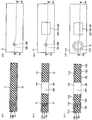
도 2의 (a1) 내지 도 2의 (c2)는 비교예의 배선 기판(50)의 제조 공정을 나타내는 도면.
도 3의 (a1) 내지 도 3의 (c2)는 비교예의 배선 기판(50)의 제조 공정을 나타내는 도면.
도 4의 (a1) 내지 도 4의 (c2)는 비교예의 배선 기판(50)의 제조 공정을 나타내는 도면.
도 5의 (a) 및 도 5의 (b)는 비교예의 배선 기판(50)의 제조 방법의 문제점을 나타내는 도면.
도 6은 비교예의 배선 기판(50)의 제조 방법의 다른 문제점을 나타내는 도면.
도 7의 (a) 내지 도 7의 (d)는 실시예에 따른 배선 기판(100)의 단면도 및 평면도.
도 8의 (a1) 내지 도 8의 (c2)는 실시예에 따른 배선 기판(100)의 제조 공정을 나타내는 도면.
도 9의 (a1) 내지 도 9의 (c2)는 실시예에 따른 배선 기판(100)의 제조 공정을 나타내는 도면.
도 10의 (a1) 내지 도 10의 (c2)는 실시예에 따른 배선 기판(100)의 제조 공정을 나타내는 도면.
도 11의 (a) 내지 도 11의 (b)는 실시예에 따른 배선 기판(100)의 이점을 나타내는 도면.
도 12는 실시예에 따른 배선 기판(100)의 다른 이점을 나타내는 도면.
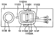
도 13은 실시예의 변형예에 따른 배선 기판(100A)의 부분 평면도.
13B : 매설용 수지 14 : 칩 커패시터
16 : 절연층 17A, 17B, 17C : 비아 전극
18A, 18B, 18C, 18D : 배선층 20A, 20B, 20C, 20D : 배선층
19A, 19B : 비아 전극 111A, 111B : 배선층
111P : 개구부 112A, 112B, 112C, 112D : 배선층
115 : 절연층 115A : 절연층
115D : 연장부
Claims (8)
- 스루홀(10P)이 관통하고 제 1 면 및 당해 제 1 면에 반대측인 제 2 면을 갖는 코어층(10),
상기 코어층(10)의 제 1 면에 형성되고 상기 스루홀(10P)과 연통하는 제 1 개구부(111P)를 갖는 제 1 배선층(111A)으로서, 상기 제 1 개구부(111P)의 개구 면적이 평면에서 볼 때 스루홀(10P)의 개구 면적보다 큰 상기 제 1 배선층(111A),
상기 스루홀(10P) 및 상기 제 1 개구부(111P) 내에 배치되고, 제 1 면, 당해 제 1 면에 반대측인 제 2 면, 및 당해 제 1 면과 당해 제 2 면 사이의 측면을 포함함과 함께, 당해 제 1 면에 한 쌍의 단자(14B, 14C)를 더 포함하는 전자 부품(14)으로서, 상기 전자 부품(14)의 제 1 면은 상기 코어층(10)의 제 1 면 측에 위치되고 상기 전자 부품(14)의 제 2 면은 상기 코어층(10)의 제 2 면 측에 위치되는 상기 전자 부품(14), 및
상기 전자 부품(14)의 제 2 면 및 측면을 덮도록, 상기 스루홀(10P), 상기 제 1 개구부(111P), 및 상기 한 쌍의 단자(14B, 14C)간의 갭에 충전되는 제 1 수지층(115)을 포함하는 배선 기판(100). - 제 1 항에 있어서,
상기 코어층(10)의 제 1 면, 상기 제 1 배선층(111A)의 표면, 및 상기 전자 부품(14)의 상기 한 쌍의 단자(14B, 14C)의 표면에 형성되는 제 2 수지층(16)을 더 포함하는 배선 기판. - 제 2 항에 있어서,
상기 제 2 수지층(16)은 상기 제 1 수지층(115)과는 상이한 수지로 이루어지는 배선 기판. - 제 1 항에 있어서,
상기 제 1 배선층(111A)은, 상기 제 1 개구부(111P)와 연통하고 평면에서 볼 때 상기 제 1 개구부(111P)로부터 바깥쪽으로 연장되는 홈(111C1)을 더 갖는 배선 기판. - 제 1 항에 있어서,
상기 제 1 배선층(111A)의 표면, 상기 한 쌍의 단자(14B, 14C)의 표면 및 상기 제 1 수지층(115)의 표면은 서로 실질적으로 동일 평면이 되는 배선 기판. - 제 1 항에 기재된 배선 기판(100), 및
상기 배선 기판(100) 상에 배치되는 반도체 소자(42)를 포함하는 반도체 디바이스. - 제 6 항에 있어서,
상기 배선 기판(100)은,
상기 코어층(10)의 제 1 면, 상기 제 1 배선층(111A)의 표면, 및 상기 전자 부품(14)의 한 쌍의 단자(14B, 14C)의 표면에 형성되는 제 2 수지층(16)을 더 포함하는 반도체 디바이스. - 제 7 항에 있어서,
상기 제 2 수지층(16)은 상기 제 1 수지층(115)과는 상이한 수지로 이루어지는 반도체 디바이스.
Applications Claiming Priority (2)
| Application Number | Priority Date | Filing Date | Title |
|---|---|---|---|
| JPJP-P-2012-190381 | 2012-08-30 | ||
| JP2012190381A JP6166878B2 (ja) | 2012-08-30 | 2012-08-30 | 配線基板、及び、配線基板の製造方法 |
Publications (2)
| Publication Number | Publication Date |
|---|---|
| KR20140029193A true KR20140029193A (ko) | 2014-03-10 |
| KR101925864B1 KR101925864B1 (ko) | 2018-12-06 |
Family
ID=50187322
Family Applications (1)
| Application Number | Title | Priority Date | Filing Date |
|---|---|---|---|
| KR1020130097016A Active KR101925864B1 (ko) | 2012-08-30 | 2013-08-16 | 배선 기판 |
Country Status (3)
| Country | Link |
|---|---|
| US (1) | US8867225B2 (ko) |
| JP (1) | JP6166878B2 (ko) |
| KR (1) | KR101925864B1 (ko) |
Families Citing this family (9)
| Publication number | Priority date | Publication date | Assignee | Title |
|---|---|---|---|---|
| JP6460439B2 (ja) * | 2014-03-31 | 2019-01-30 | 京セラ株式会社 | 印刷配線板およびその製造方法 |
| US9640521B2 (en) | 2014-09-30 | 2017-05-02 | Taiwan Semiconductor Manufacturing Company, Ltd. | Multi-die package with bridge layer and method for making the same |
| JP6490412B2 (ja) * | 2014-12-01 | 2019-03-27 | 株式会社東芝 | 電子機器 |
| KR102356810B1 (ko) * | 2015-01-22 | 2022-01-28 | 삼성전기주식회사 | 전자부품내장형 인쇄회로기판 및 그 제조방법 |
| JP6487257B2 (ja) * | 2015-03-31 | 2019-03-20 | 出光ユニテック株式会社 | ジッパーテープ体およびジッパーテープ付袋体の製造方法 |
| JP6487256B2 (ja) * | 2015-03-31 | 2019-03-20 | 出光ユニテック株式会社 | ジッパーテープ付袋体の製造方法 |
| JP6639934B2 (ja) | 2016-02-08 | 2020-02-05 | 新光電気工業株式会社 | 配線基板、半導体装置及び配線基板の製造方法 |
| US11871524B2 (en) | 2016-09-09 | 2024-01-09 | Fujikura Ltd. | Component-incorporated substrate and method for manufacturing same |
| US11270920B2 (en) * | 2018-08-14 | 2022-03-08 | Medtronic, Inc. | Integrated circuit package and method of forming same |
Family Cites Families (7)
| Publication number | Priority date | Publication date | Assignee | Title |
|---|---|---|---|---|
| JP2001217514A (ja) * | 2000-02-03 | 2001-08-10 | Denso Corp | 多層配線基板 |
| JP4726546B2 (ja) | 2005-06-03 | 2011-07-20 | 日本特殊陶業株式会社 | 配線基板の製造方法 |
| EP1729552A3 (en) | 2005-06-03 | 2009-01-07 | Ngk Spark Plug Co., Ltd. | Wiring board and manufacturing method of wiring board |
| WO2010018708A1 (ja) * | 2008-08-12 | 2010-02-18 | 株式会社村田製作所 | 部品内蔵モジュールの製造方法及び部品内蔵モジュール |
| JP2010171413A (ja) * | 2008-12-26 | 2010-08-05 | Ngk Spark Plug Co Ltd | 部品内蔵配線基板の製造方法 |
| JP5001395B2 (ja) * | 2010-03-31 | 2012-08-15 | イビデン株式会社 | 配線板及び配線板の製造方法 |
| KR101085733B1 (ko) * | 2010-05-28 | 2011-11-21 | 삼성전기주식회사 | 전자소자 내장 인쇄회로기판 및 그 제조방법 |
-
2012
- 2012-08-30 JP JP2012190381A patent/JP6166878B2/ja active Active
-
2013
- 2013-08-16 KR KR1020130097016A patent/KR101925864B1/ko active Active
- 2013-08-22 US US13/973,346 patent/US8867225B2/en active Active
Also Published As
| Publication number | Publication date |
|---|---|
| JP6166878B2 (ja) | 2017-07-19 |
| KR101925864B1 (ko) | 2018-12-06 |
| US8867225B2 (en) | 2014-10-21 |
| JP2014049558A (ja) | 2014-03-17 |
| US20140063763A1 (en) | 2014-03-06 |
Similar Documents
| Publication | Publication Date | Title |
|---|---|---|
| KR20140029193A (ko) | 배선 기판 | |
| US8419884B2 (en) | Method for manufacturing multilayer wiring substrate | |
| US8559184B2 (en) | Electronic component built-in substrate and method of manufacturing the same | |
| US9773747B2 (en) | Wiring substrate and method for manufacturing wiring subtrate | |
| US9288910B2 (en) | Substrate with built-in electronic component and method for manufacturing substrate with built-in electronic component | |
| US11812556B2 (en) | Printed circuit board and manufacturing method thereof | |
| KR101514518B1 (ko) | 전자부품 내장 인쇄회로기판 및 그 제조방법 | |
| KR101025524B1 (ko) | 배선 기판 및 그 제조 방법 | |
| JP5989814B2 (ja) | 埋め込み基板、印刷回路基板及びその製造方法 | |
| CN102090159A (zh) | 刚挠性电路板以及其电子设备 | |
| US20160021744A1 (en) | Printed circuit board and method of manufacturing the same | |
| KR20080019282A (ko) | 회로 보드 구조체 제조 방법 및 회로 보드 구조체 | |
| US20140116763A1 (en) | Wiring board with built-in electronic component and method for manufacturing the same | |
| US20140116767A1 (en) | Wiring board with built-in electronic component and method for manufacturing the same | |
| KR20130135097A (ko) | 전자 부품 내장 기판 및 그 제조 방법 | |
| KR101003341B1 (ko) | 코어 기판 및 그 제조 방법 | |
| US20140318834A1 (en) | Wiring board and method for manufacturing the same | |
| KR20170001388A (ko) | 인쇄회로기판 및 인쇄회로기판의 제조 방법 | |
| US8737085B2 (en) | Wiring board with a built-in component and method for manufacturing the same | |
| KR20160090625A (ko) | 전자소자내장형 인쇄회로기판 및 그 제조방법 | |
| KR20180128766A (ko) | 전자부품 내장 인쇄회로기판 | |
| US9420696B2 (en) | Method of manufacturing wiring substrate | |
| KR102281460B1 (ko) | 임베디드 기판 및 임베디드 기판의 제조 방법 | |
| KR20160010996A (ko) | 인쇄회로기판 및 인쇄회로기판의 제조 방법 | |
| KR20160079658A (ko) | 배선 기판의 제조 방법 |
Legal Events
| Date | Code | Title | Description |
|---|---|---|---|
| PA0109 | Patent application |
St.27 status event code: A-0-1-A10-A12-nap-PA0109 |
|
| PG1501 | Laying open of application |
St.27 status event code: A-1-1-Q10-Q12-nap-PG1501 |
|
| A201 | Request for examination | ||
| E13-X000 | Pre-grant limitation requested |
St.27 status event code: A-2-3-E10-E13-lim-X000 |
|
| P11-X000 | Amendment of application requested |
St.27 status event code: A-2-2-P10-P11-nap-X000 |
|
| P13-X000 | Application amended |
St.27 status event code: A-2-2-P10-P13-nap-X000 |
|
| PA0201 | Request for examination |
St.27 status event code: A-1-2-D10-D11-exm-PA0201 |
|
| R17-X000 | Change to representative recorded |
St.27 status event code: A-3-3-R10-R17-oth-X000 |
|
| E701 | Decision to grant or registration of patent right | ||
| PE0701 | Decision of registration |
St.27 status event code: A-1-2-D10-D22-exm-PE0701 |
|
| GRNT | Written decision to grant | ||
| PR0701 | Registration of establishment |
St.27 status event code: A-2-4-F10-F11-exm-PR0701 |
|
| PR1002 | Payment of registration fee |
St.27 status event code: A-2-2-U10-U11-oth-PR1002 Fee payment year number: 1 |
|
| PG1601 | Publication of registration |
St.27 status event code: A-4-4-Q10-Q13-nap-PG1601 |
|
| FPAY | Annual fee payment |
Payment date: 20211027 Year of fee payment: 4 |
|
| PR1001 | Payment of annual fee |
St.27 status event code: A-4-4-U10-U11-oth-PR1001 Fee payment year number: 4 |
|
| FPAY | Annual fee payment |
Payment date: 20221017 Year of fee payment: 5 |
|
| PR1001 | Payment of annual fee |
St.27 status event code: A-4-4-U10-U11-oth-PR1001 Fee payment year number: 5 |
|
| PR1001 | Payment of annual fee |
St.27 status event code: A-4-4-U10-U11-oth-PR1001 Fee payment year number: 6 |
|
| PR1001 | Payment of annual fee |
St.27 status event code: A-4-4-U10-U11-oth-PR1001 Fee payment year number: 7 |
|
| PR1001 | Payment of annual fee |
St.27 status event code: A-4-4-U10-U11-oth-PR1001 Fee payment year number: 8 |
|
| U11 | Full renewal or maintenance fee paid |
Free format text: ST27 STATUS EVENT CODE: A-4-4-U10-U11-OTH-PR1001 (AS PROVIDED BY THE NATIONAL OFFICE) Year of fee payment: 8 |