KR20140031908A - 반도체 기판 프로세싱 시스템 - Google Patents
반도체 기판 프로세싱 시스템 Download PDFInfo
- Publication number
- KR20140031908A KR20140031908A KR1020137031080A KR20137031080A KR20140031908A KR 20140031908 A KR20140031908 A KR 20140031908A KR 1020137031080 A KR1020137031080 A KR 1020137031080A KR 20137031080 A KR20137031080 A KR 20137031080A KR 20140031908 A KR20140031908 A KR 20140031908A
- Authority
- KR
- South Korea
- Prior art keywords
- chamber
- substrate
- transfer chamber
- gas
- processing system
- Prior art date
- Legal status (The legal status is an assumption and is not a legal conclusion. Google has not performed a legal analysis and makes no representation as to the accuracy of the status listed.)
- Granted
Links
Images




Classifications
-
- C—CHEMISTRY; METALLURGY
- C23—COATING METALLIC MATERIAL; COATING MATERIAL WITH METALLIC MATERIAL; CHEMICAL SURFACE TREATMENT; DIFFUSION TREATMENT OF METALLIC MATERIAL; COATING BY VACUUM EVAPORATION, BY SPUTTERING, BY ION IMPLANTATION OR BY CHEMICAL VAPOUR DEPOSITION, IN GENERAL; INHIBITING CORROSION OF METALLIC MATERIAL OR INCRUSTATION IN GENERAL
- C23C—COATING METALLIC MATERIAL; COATING MATERIAL WITH METALLIC MATERIAL; SURFACE TREATMENT OF METALLIC MATERIAL BY DIFFUSION INTO THE SURFACE, BY CHEMICAL CONVERSION OR SUBSTITUTION; COATING BY VACUUM EVAPORATION, BY SPUTTERING, BY ION IMPLANTATION OR BY CHEMICAL VAPOUR DEPOSITION, IN GENERAL
- C23C16/00—Chemical coating by decomposition of gaseous compounds, without leaving reaction products of surface material in the coating, i.e. chemical vapour deposition [CVD] processes
- C23C16/06—Chemical coating by decomposition of gaseous compounds, without leaving reaction products of surface material in the coating, i.e. chemical vapour deposition [CVD] processes characterised by the deposition of metallic material
-
- C—CHEMISTRY; METALLURGY
- C23—COATING METALLIC MATERIAL; COATING MATERIAL WITH METALLIC MATERIAL; CHEMICAL SURFACE TREATMENT; DIFFUSION TREATMENT OF METALLIC MATERIAL; COATING BY VACUUM EVAPORATION, BY SPUTTERING, BY ION IMPLANTATION OR BY CHEMICAL VAPOUR DEPOSITION, IN GENERAL; INHIBITING CORROSION OF METALLIC MATERIAL OR INCRUSTATION IN GENERAL
- C23C—COATING METALLIC MATERIAL; COATING MATERIAL WITH METALLIC MATERIAL; SURFACE TREATMENT OF METALLIC MATERIAL BY DIFFUSION INTO THE SURFACE, BY CHEMICAL CONVERSION OR SUBSTITUTION; COATING BY VACUUM EVAPORATION, BY SPUTTERING, BY ION IMPLANTATION OR BY CHEMICAL VAPOUR DEPOSITION, IN GENERAL
- C23C16/00—Chemical coating by decomposition of gaseous compounds, without leaving reaction products of surface material in the coating, i.e. chemical vapour deposition [CVD] processes
- C23C16/22—Chemical coating by decomposition of gaseous compounds, without leaving reaction products of surface material in the coating, i.e. chemical vapour deposition [CVD] processes characterised by the deposition of inorganic material, other than metallic material
- C23C16/30—Deposition of compounds, mixtures or solid solutions, e.g. borides, carbides, nitrides
- C23C16/301—AIII BV compounds, where A is Al, Ga, In or Tl and B is N, P, As, Sb or Bi
-
- C—CHEMISTRY; METALLURGY
- C23—COATING METALLIC MATERIAL; COATING MATERIAL WITH METALLIC MATERIAL; CHEMICAL SURFACE TREATMENT; DIFFUSION TREATMENT OF METALLIC MATERIAL; COATING BY VACUUM EVAPORATION, BY SPUTTERING, BY ION IMPLANTATION OR BY CHEMICAL VAPOUR DEPOSITION, IN GENERAL; INHIBITING CORROSION OF METALLIC MATERIAL OR INCRUSTATION IN GENERAL
- C23C—COATING METALLIC MATERIAL; COATING MATERIAL WITH METALLIC MATERIAL; SURFACE TREATMENT OF METALLIC MATERIAL BY DIFFUSION INTO THE SURFACE, BY CHEMICAL CONVERSION OR SUBSTITUTION; COATING BY VACUUM EVAPORATION, BY SPUTTERING, BY ION IMPLANTATION OR BY CHEMICAL VAPOUR DEPOSITION, IN GENERAL
- C23C16/00—Chemical coating by decomposition of gaseous compounds, without leaving reaction products of surface material in the coating, i.e. chemical vapour deposition [CVD] processes
- C23C16/44—Chemical coating by decomposition of gaseous compounds, without leaving reaction products of surface material in the coating, i.e. chemical vapour deposition [CVD] processes characterised by the method of coating
- C23C16/4412—Details relating to the exhausts, e.g. pumps, filters, scrubbers, particle traps
-
- C—CHEMISTRY; METALLURGY
- C23—COATING METALLIC MATERIAL; COATING MATERIAL WITH METALLIC MATERIAL; CHEMICAL SURFACE TREATMENT; DIFFUSION TREATMENT OF METALLIC MATERIAL; COATING BY VACUUM EVAPORATION, BY SPUTTERING, BY ION IMPLANTATION OR BY CHEMICAL VAPOUR DEPOSITION, IN GENERAL; INHIBITING CORROSION OF METALLIC MATERIAL OR INCRUSTATION IN GENERAL
- C23C—COATING METALLIC MATERIAL; COATING MATERIAL WITH METALLIC MATERIAL; SURFACE TREATMENT OF METALLIC MATERIAL BY DIFFUSION INTO THE SURFACE, BY CHEMICAL CONVERSION OR SUBSTITUTION; COATING BY VACUUM EVAPORATION, BY SPUTTERING, BY ION IMPLANTATION OR BY CHEMICAL VAPOUR DEPOSITION, IN GENERAL
- C23C16/00—Chemical coating by decomposition of gaseous compounds, without leaving reaction products of surface material in the coating, i.e. chemical vapour deposition [CVD] processes
- C23C16/44—Chemical coating by decomposition of gaseous compounds, without leaving reaction products of surface material in the coating, i.e. chemical vapour deposition [CVD] processes characterised by the method of coating
- C23C16/455—Chemical coating by decomposition of gaseous compounds, without leaving reaction products of surface material in the coating, i.e. chemical vapour deposition [CVD] processes characterised by the method of coating characterised by the method used for introducing gases into reaction chamber or for modifying gas flows in reaction chamber
- C23C16/45563—Gas nozzles
- C23C16/45565—Shower nozzles
-
- C—CHEMISTRY; METALLURGY
- C23—COATING METALLIC MATERIAL; COATING MATERIAL WITH METALLIC MATERIAL; CHEMICAL SURFACE TREATMENT; DIFFUSION TREATMENT OF METALLIC MATERIAL; COATING BY VACUUM EVAPORATION, BY SPUTTERING, BY ION IMPLANTATION OR BY CHEMICAL VAPOUR DEPOSITION, IN GENERAL; INHIBITING CORROSION OF METALLIC MATERIAL OR INCRUSTATION IN GENERAL
- C23C—COATING METALLIC MATERIAL; COATING MATERIAL WITH METALLIC MATERIAL; SURFACE TREATMENT OF METALLIC MATERIAL BY DIFFUSION INTO THE SURFACE, BY CHEMICAL CONVERSION OR SUBSTITUTION; COATING BY VACUUM EVAPORATION, BY SPUTTERING, BY ION IMPLANTATION OR BY CHEMICAL VAPOUR DEPOSITION, IN GENERAL
- C23C16/00—Chemical coating by decomposition of gaseous compounds, without leaving reaction products of surface material in the coating, i.e. chemical vapour deposition [CVD] processes
- C23C16/44—Chemical coating by decomposition of gaseous compounds, without leaving reaction products of surface material in the coating, i.e. chemical vapour deposition [CVD] processes characterised by the method of coating
- C23C16/455—Chemical coating by decomposition of gaseous compounds, without leaving reaction products of surface material in the coating, i.e. chemical vapour deposition [CVD] processes characterised by the method of coating characterised by the method used for introducing gases into reaction chamber or for modifying gas flows in reaction chamber
- C23C16/45563—Gas nozzles
- C23C16/45574—Nozzles for more than one gas
-
- C—CHEMISTRY; METALLURGY
- C23—COATING METALLIC MATERIAL; COATING MATERIAL WITH METALLIC MATERIAL; CHEMICAL SURFACE TREATMENT; DIFFUSION TREATMENT OF METALLIC MATERIAL; COATING BY VACUUM EVAPORATION, BY SPUTTERING, BY ION IMPLANTATION OR BY CHEMICAL VAPOUR DEPOSITION, IN GENERAL; INHIBITING CORROSION OF METALLIC MATERIAL OR INCRUSTATION IN GENERAL
- C23C—COATING METALLIC MATERIAL; COATING MATERIAL WITH METALLIC MATERIAL; SURFACE TREATMENT OF METALLIC MATERIAL BY DIFFUSION INTO THE SURFACE, BY CHEMICAL CONVERSION OR SUBSTITUTION; COATING BY VACUUM EVAPORATION, BY SPUTTERING, BY ION IMPLANTATION OR BY CHEMICAL VAPOUR DEPOSITION, IN GENERAL
- C23C16/00—Chemical coating by decomposition of gaseous compounds, without leaving reaction products of surface material in the coating, i.e. chemical vapour deposition [CVD] processes
- C23C16/44—Chemical coating by decomposition of gaseous compounds, without leaving reaction products of surface material in the coating, i.e. chemical vapour deposition [CVD] processes characterised by the method of coating
- C23C16/54—Apparatus specially adapted for continuous coating
-
- H—ELECTRICITY
- H10—SEMICONDUCTOR DEVICES; ELECTRIC SOLID-STATE DEVICES NOT OTHERWISE PROVIDED FOR
- H10P—GENERIC PROCESSES OR APPARATUS FOR THE MANUFACTURE OR TREATMENT OF DEVICES COVERED BY CLASS H10
- H10P72/00—Handling or holding of wafers, substrates or devices during manufacture or treatment thereof
- H10P72/04—Apparatus for manufacture or treatment
- H10P72/0431—Apparatus for thermal treatment
- H10P72/0436—Apparatus for thermal treatment mainly by radiation
-
- H—ELECTRICITY
- H10—SEMICONDUCTOR DEVICES; ELECTRIC SOLID-STATE DEVICES NOT OTHERWISE PROVIDED FOR
- H10P—GENERIC PROCESSES OR APPARATUS FOR THE MANUFACTURE OR TREATMENT OF DEVICES COVERED BY CLASS H10
- H10P72/00—Handling or holding of wafers, substrates or devices during manufacture or treatment thereof
- H10P72/04—Apparatus for manufacture or treatment
- H10P72/0451—Apparatus for manufacturing or treating in a plurality of work-stations
- H10P72/0461—Apparatus for manufacturing or treating in a plurality of work-stations characterised by the presence of two or more transfer chambers
-
- H—ELECTRICITY
- H10—SEMICONDUCTOR DEVICES; ELECTRIC SOLID-STATE DEVICES NOT OTHERWISE PROVIDED FOR
- H10P—GENERIC PROCESSES OR APPARATUS FOR THE MANUFACTURE OR TREATMENT OF DEVICES COVERED BY CLASS H10
- H10P72/00—Handling or holding of wafers, substrates or devices during manufacture or treatment thereof
- H10P72/04—Apparatus for manufacture or treatment
- H10P72/0451—Apparatus for manufacturing or treating in a plurality of work-stations
- H10P72/0466—Apparatus for manufacturing or treating in a plurality of work-stations characterised by the construction of the load-lock chamber
-
- H—ELECTRICITY
- H10—SEMICONDUCTOR DEVICES; ELECTRIC SOLID-STATE DEVICES NOT OTHERWISE PROVIDED FOR
- H10P—GENERIC PROCESSES OR APPARATUS FOR THE MANUFACTURE OR TREATMENT OF DEVICES COVERED BY CLASS H10
- H10P72/00—Handling or holding of wafers, substrates or devices during manufacture or treatment thereof
- H10P72/04—Apparatus for manufacture or treatment
- H10P72/0451—Apparatus for manufacturing or treating in a plurality of work-stations
- H10P72/0468—Apparatus for manufacturing or treating in a plurality of work-stations comprising a chamber adapted to a particular process
Landscapes
- Chemical & Material Sciences (AREA)
- General Chemical & Material Sciences (AREA)
- Chemical Kinetics & Catalysis (AREA)
- Engineering & Computer Science (AREA)
- Materials Engineering (AREA)
- Mechanical Engineering (AREA)
- Metallurgy (AREA)
- Organic Chemistry (AREA)
- Inorganic Chemistry (AREA)
- Chemical Vapour Deposition (AREA)
- Drying Of Semiconductors (AREA)
- Health & Medical Sciences (AREA)
- Toxicology (AREA)
Abstract
Description
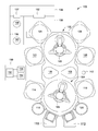
도 1은 본원에서 개시되는 프로세스들을 수행하도록 적응될 수 있는 다중-챔버(multi-chamber) 프로세싱 시스템의 개략적 상부도를 도시한다.
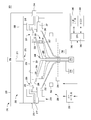
도 2는 본 발명의 일부 실시예들에 따른 프로세스 챔버의 개략적 측면도를 도시한다.
도 3은 본 발명의 일부 실시예들에 따른 도 2의 프로세스 챔버의 주입기 및 배기포트의 부분적인 개략적 상부도를 도시한다.
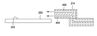
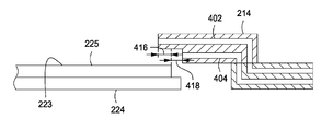
도 4a-c는 본 발명의 일부 실시예들에 따른 주입기들의 개략적인 정면 및 측면도들을 각각 도시한다.
도 5a-b는 본 발명의 일부 실시예들에 따른 주입기들의 개략적인 정면도들을 각각 도시한다.
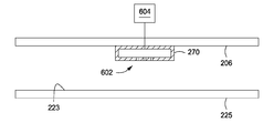
도 6은 본 발명의 일부 실시예들에 따른 샤워헤드의 개략적인 측면도를 도시한다.
이해를 용이하게 하기 위하여, 도면들에서 공통되는 동일한 요소들을 표시하기 위해 가능한 한 동일한 참조번호들이 사용되었다. 도면들은 일정한 비율로 도시된 것은 아니며, 명료함을 위해 단순화될 수 있다. 일 실시예의 요소들 및 특징들은 추가의 언급없이 다른 실시예들에 유리하게 통합될 수 있음이 고려된다.


Claims (15)
- 프로세싱 시스템으로서,
제 1 이송 챔버 ― 상기 제 1 이송 챔버는 상기 제 1 이송 챔버에 커플링된 하나 또는 둘 이상의 프로세스 챔버들에 기판을 이송하거나 상기 하나 또는 둘 이상의 프로세스 챔버들로부터 기판을 받을 수 있음 ― ; 및
상기 제 1 이송 챔버에 커플링된, 하나 또는 둘 이상의 Ⅲ-Ⅴ 재료들을 증착하기 위한 제 1 프로세스 챔버를 포함하며,
상기 제 1 프로세스 챔버는,
상기 프로세스 챔버 내의 요구되는 위치에 기판의 프로세싱 표면을 지지하기 위해 상기 제 1 프로세스 챔버 내에 배치되는 기판 지지체;
상기 기판 지지체의 제 1 측면에 배치되며, 제 1 프로세스 가스를 제공하기 위한 제 1 유동 경로 및 상기 제 1 프로세스 가스와 별개의 제 2 프로세스 가스를 제공하기 위한 제 2 유동 경로를 갖는 주입기(injector) ― 상기 주입기는 상기 기판의 상기 프로세싱 표면 전체에 걸쳐서 상기 제 1 프로세스 가스 및 상기 제 2 프로세스 가스를 제공하도록 위치됨 ― ; 및
상기 프로세스 챔버로부터 상기 제 1 프로세스 가스 및 상기 제 2 프로세스 가스를 배기하기 위해, 상기 주입기 반대편의, 상기 기판 지지체의 제 2 측면에 배치되는 배기 포트를 더 포함하며; 그리고
상기 제 1 프로세스 챔버는,
상기 기판 지지체 위에 배치되어, 상기 기판의 상기 프로세싱 표면에 상기 제 1 프로세스 가스를 제공하는 샤워헤드; 또는
상기 주입기에 커플링되어 상기 제 1 프로세스 가스를 제공하는 제 1 가스 소스 및 상기 주입기에 커플링되어 상기 제 2 프로세스 가스를 제공하는 제 2 가스 소스 ― 상기 제 1 프로세스 가스는 Ⅲ족 원소를 포함하고, 상기 제 2 프로세스 가스는 Ⅴ족 원소를 포함함 ― ;
중에서 하나 또는 둘 이상을 더 포함하는,
프로세싱 시스템. - 제 1 항에 있어서,
상기 제 1 프로세스 챔버는 상기 샤워헤드, 상기 제 1 가스 소스 및 상기 제 2 가스 소스를 포함하는,
프로세싱 시스템. - 제 1 항 또는 제 2 항에 있어서,
제 2 이송 챔버; 및
상기 제 2 이송 챔버를 상기 제 1 이송 챔버에 커플링하는 하나 또는 둘 이상의 중간 로드락 챔버들을 더 포함하는,
프로세싱 시스템. - 제 3 항에 있어서,
기판이 상기 하나 또는 둘 이상의 중간 로드락 챔버들 내에 배치될 때 상기 기판을 가스에 노출시키기 위해, 상기 하나 또는 둘 이상의 중간 로드락 챔버들에 커플링되는 가스 소스를 더 포함하는,
프로세싱 시스템. - 제 3 항에 있어서,
상기 제 1 이송 챔버 및 상기 제 2 이송 챔버는 하나 또는 둘 이상의 독립적으로 제어되는 챔버 파라미터들을 갖는,
프로세싱 시스템. - 제 5 항에 있어서,
상기 하나 또는 둘 이상의 독립적으로 제어되는 챔버 파라미터들은, 압력, 퍼지 가스 유동, 수분 레벨, 또는 잔여 가스 레벨 중에서 하나 또는 둘 이상을 포함하는,
프로세싱 시스템. - 제 3 항에 있어서,
기판을 플라즈마 세정하기 위한 제 2 프로세스 챔버; 및
하이-k 유전 재료를 증착하기 위한 제 3 프로세스 챔버를 더 포함하며,
상기 제 2 프로세스 챔버 및 상기 제 3 프로세스 챔버는 상기 제 2 이송 챔버에 커플링되는,
프로세싱 시스템. - 제 7 항에 있어서,
기판을 어닐링하기 위한 제 4 프로세스 챔버를 더 포함하며,
상기 제 4 프로세스 챔버는 상기 제 1 이송 챔버에 커플링되는,
프로세싱 시스템. - 제 8 항에 있어서,
상기 제 1 이송 챔버에 커플링되는, 하나 또는 둘 이상의 Ⅲ-Ⅴ 재료들을 증착하기 위한 제 5 프로세스 챔버를 더 포함하는,
프로세싱 시스템. - 제 9 항에 있어서,
상기 제 1 프로세스 챔버는 n-타입 Ⅲ-Ⅴ 재료들을 증착하고, 상기 제 5 프로세스 챔버는 p-타입 Ⅲ-Ⅴ 재료들을 증착하는,
프로세싱 시스템. - 제 1 항 또는 제 2 항에 있어서,
상기 제 1 프로세스 챔버는,
상기 제 1 프로세스 챔버를 둘러싸며 그리고 하우스 배기 시스템(house exhaust system)으로 환기하는(ventilating) 제 1 엔클로저(enclosure); 및
상기 제 1 엔클로저 근처에 배치되는 제 2 엔클로저 ― 상기 제 1 엔클로저는 상기 제 1 엔클로저와 상기 제 2 엔클로저 사이의 액세스 포트를 통해 상기 제 2 엔클로저에 대해 선택적으로 개방됨 ―;
를 더 포함하는,
프로세싱 시스템. - Ⅲ-Ⅴ 재료들을 증착하기 위한 프로세싱 시스템으로서,
제 1 이송 챔버 ― 상기 제 1 이송 챔버는, 상기 제 1 이송 챔버에 커플링된 프로세스 챔버들 사이에서 기판들을 이송하도록 구성된 제 1 로봇을 가짐 ― ;
제 2 이송 챔버 ― 상기 제 2 이송 챔버는, 상기 제 2 이송 챔버에 커플링된 프로세스 챔버들 사이에서 기판들을 이송하도록 구성된 제 2 로봇을 가짐 ― ;
상기 제 1 이송 챔버와 상기 제 2 이송 챔버 내의 챔버 파라미터들이 독립적으로 제어되도록, 상기 제 1 이송 챔버와 상기 제 2 이송 챔버 사이에 배치되어, 상기 제 1 이송 챔버를 상기 제 2 이송 챔버에 커플링하는 하나 또는 둘 이상의 중간 로드락들(loadlocks);
상기 제 1 이송 챔버에 커플링된, Ⅲ-Ⅴ 재료들을 증착하기 위한 제 1 프로세스 챔버;
상기 제 2 이송 챔버에 커플링되며, 기판 상에서 플라즈마 세정을 하거나 기판 상에 하이-k 유전체를 증착하도록 각각 구성되는 제 2 프로세스 챔버 또는 제 3 프로세스 챔버 중에서 하나 또는 둘 이상;
상기 제 1 이송 챔버에 커플링되며, 기판을 어닐링하거나 Ⅲ-Ⅴ 재료들을 증착하도록 각각 구성되는 제 4 프로세스 챔버 또는 제 5 프로세스 챔버 중에서 하나 또는 둘 이상; 및
상기 제 2 이송 챔버에 커플링되며, 클러스터 툴 내로의 기판의 진입(entry) 또는 상기 클러스터 툴로부터의 기판의 퇴거(egress)를 용이하게 하도록 구성되는 하나 또는 둘 이상의 제 2 로드락 챔버들을 포함하는,
프로세싱 시스템. - 제 12 항에 있어서,
기판이 상기 하나 또는 둘 이상의 중간 로드락 챔버들 내에 배치될 때 상기 기판을 가스에 노출시키기 위해, 상기 하나 또는 둘 이상의 중간 로드락 챔버들에 커플링되는 가스 소스를 더 포함하는,
프로세싱 시스템. - 제 12 항에 있어서,
상기 하나 또는 둘 이상의 독립적으로 제어되는 챔버 파라미터들은, 압력, 퍼지 가스 유동, 수분 레벨, 또는 잔여 가스 레벨 중에서 하나 또는 둘 이상을 포함하는,
프로세싱 시스템. - 제 12 항 내지 제 14 항 중 어느 한 항에 있어서,
상기 제 1 프로세스 챔버 및 상기 제 5 프로세스 챔버는, 각각, n-타입 Ⅲ-Ⅴ 재료들 및 p-타입 Ⅲ-Ⅴ 재료들을 증착하도록 구성되는,
프로세싱 시스템.
Applications Claiming Priority (5)
| Application Number | Priority Date | Filing Date | Title |
|---|---|---|---|
| US201161478776P | 2011-04-25 | 2011-04-25 | |
| US61/478,776 | 2011-04-25 | ||
| US13/441,382 | 2012-04-06 | ||
| US13/441,382 US9512520B2 (en) | 2011-04-25 | 2012-04-06 | Semiconductor substrate processing system |
| PCT/US2012/034374 WO2012148801A2 (en) | 2011-04-25 | 2012-04-20 | Semiconductor substrate processing system |
Publications (2)
| Publication Number | Publication Date |
|---|---|
| KR20140031908A true KR20140031908A (ko) | 2014-03-13 |
| KR101888366B1 KR101888366B1 (ko) | 2018-08-14 |
Family
ID=47020284
Family Applications (1)
| Application Number | Title | Priority Date | Filing Date |
|---|---|---|---|
| KR1020137031080A Active KR101888366B1 (ko) | 2011-04-25 | 2012-04-20 | 반도체 기판 프로세싱 시스템 |
Country Status (7)
| Country | Link |
|---|---|
| US (1) | US9512520B2 (ko) |
| KR (1) | KR101888366B1 (ko) |
| CN (1) | CN103493180B (ko) |
| DE (1) | DE112012001864T5 (ko) |
| SG (1) | SG194144A1 (ko) |
| TW (1) | TWI594351B (ko) |
| WO (1) | WO2012148801A2 (ko) |
Cited By (3)
| Publication number | Priority date | Publication date | Assignee | Title |
|---|---|---|---|---|
| KR20170048562A (ko) * | 2014-09-05 | 2017-05-08 | 어플라이드 머티어리얼스, 인코포레이티드 | Epi 챔버를 위한 주입 인서트 |
| KR20190004362A (ko) * | 2016-06-01 | 2019-01-11 | 어플라이드 머티어리얼스, 인코포레이티드 | 3d 낸드 응용들을 위한 터널 산화물의 고압 암모니아 질화 |
| KR20220156911A (ko) * | 2020-08-03 | 2022-11-28 | 어플라이드 머티어리얼스, 인코포레이티드 | 뱃치 열 프로세스 챔버에서 웨이퍼 에지 온도 보정 |
Families Citing this family (37)
| Publication number | Priority date | Publication date | Assignee | Title |
|---|---|---|---|---|
| US20120270384A1 (en) * | 2011-04-22 | 2012-10-25 | Applied Materials, Inc. | Apparatus for deposition of materials on a substrate |
| US9512520B2 (en) * | 2011-04-25 | 2016-12-06 | Applied Materials, Inc. | Semiconductor substrate processing system |
| US9499905B2 (en) * | 2011-07-22 | 2016-11-22 | Applied Materials, Inc. | Methods and apparatus for the deposition of materials on a substrate |
| CN107354428B (zh) * | 2012-07-02 | 2020-10-20 | 应用材料公司 | 用于制造装置的方法和设备 |
| TW201408811A (zh) * | 2012-08-28 | 2014-03-01 | Univ St Johns | 多流向原子層沈積系統 |
| US9532401B2 (en) * | 2013-03-15 | 2016-12-27 | Applied Materials, Inc. | Susceptor support shaft with uniformity tuning lenses for EPI process |
| TWI648427B (zh) * | 2013-07-17 | 2019-01-21 | 應用材料股份有限公司 | 用於交叉流動類型的熱cvd腔室之改良的氣體活化的結構 |
| KR102127715B1 (ko) * | 2013-08-09 | 2020-06-29 | 에스케이실트론 주식회사 | 에피텍셜 반응기 |
| JP6456956B2 (ja) * | 2013-08-19 | 2019-01-23 | アプライド マテリアルズ インコーポレイテッドApplied Materials,Incorporated | 不純物が積層したエピタキシーのための装置 |
| US10047457B2 (en) | 2013-09-16 | 2018-08-14 | Applied Materials, Inc. | EPI pre-heat ring |
| WO2015123022A1 (en) * | 2014-02-14 | 2015-08-20 | Applied Materials, Inc. | Upper dome with injection assembly |
| JP6271322B2 (ja) * | 2014-03-31 | 2018-01-31 | 東京エレクトロン株式会社 | 基板処理システム |
| US10249511B2 (en) | 2014-06-27 | 2019-04-02 | Lam Research Corporation | Ceramic showerhead including central gas injector for tunable convective-diffusive gas flow in semiconductor substrate processing apparatus |
| US9920844B2 (en) * | 2014-11-26 | 2018-03-20 | Lam Research Corporation | Valve manifold deadleg elimination via reentrant flow path |
| TWI677046B (zh) * | 2015-04-23 | 2019-11-11 | 美商應用材料股份有限公司 | 半導體處理系統中的外部基板材旋轉 |
| CN107690487B (zh) * | 2015-06-12 | 2021-03-09 | 应用材料公司 | 用于半导体外延生长的注射器 |
| US10770272B2 (en) * | 2016-04-11 | 2020-09-08 | Applied Materials, Inc. | Plasma-enhanced anneal chamber for wafer outgassing |
| US10260149B2 (en) * | 2016-04-28 | 2019-04-16 | Applied Materials, Inc. | Side inject nozzle design for processing chamber |
| CN107644949B (zh) * | 2016-07-21 | 2020-11-24 | Ncd有限公司 | 在oled上形成无机薄层的方法 |
| CN110622298B (zh) | 2017-05-13 | 2023-09-22 | 应用材料公司 | 用于高质量间隙填充方案的循环可流动沉积和高密度等离子体处理处理 |
| US10770314B2 (en) * | 2017-05-31 | 2020-09-08 | Taiwan Semiconductor Manufacturing Company, Ltd. | Semiconductor device, tool, and method of manufacturing |
| KR20200035186A (ko) * | 2017-08-30 | 2020-04-01 | 어플라이드 머티어리얼스, 인코포레이티드 | 통합 에피택시 시스템 고온 오염물 제거 |
| EP3707746B1 (en) * | 2017-11-11 | 2023-12-27 | Micromaterials LLC | Gas delivery system for high pressure processing chamber |
| JP7034817B2 (ja) * | 2018-04-19 | 2022-03-14 | 株式会社日本製鋼所 | レーザ処理装置及び半導体装置の製造方法 |
| WO2020046567A1 (en) * | 2018-08-29 | 2020-03-05 | Applied Materials, Inc. | Chamber injector |
| US11486038B2 (en) | 2019-01-30 | 2022-11-01 | Applied Materials, Inc. | Asymmetric injection for better wafer uniformity |
| FI129627B (en) * | 2019-06-28 | 2022-05-31 | Beneq Oy | Nuclear layer cultivation equipment |
| FI129578B (en) | 2019-06-28 | 2022-05-13 | Beneq Oy | Atomic layer growth equipment |
| CN114599816B (zh) | 2019-09-09 | 2024-10-29 | 应用材料公司 | 输送反应物气体的处理系统和方法 |
| US12588451B2 (en) * | 2020-04-09 | 2026-03-24 | Applied Materials, Inc. | Bottom purge for semiconductor processing system |
| US20210375650A1 (en) * | 2020-06-01 | 2021-12-02 | Applied Materials, Inc. | High temperature and vacuum isolation processing mini-environments |
| KR102760892B1 (ko) * | 2021-01-29 | 2025-02-03 | 주성엔지니어링(주) | 기판처리장치 |
| CN115161623A (zh) | 2021-03-18 | 2022-10-11 | Asm Ip私人控股有限公司 | 用于膜沉积期间衬底温度控制的双高温计系统 |
| KR20220130621A (ko) | 2021-03-18 | 2022-09-27 | 에이에스엠 아이피 홀딩 비.브이. | 램프 뱅크 정렬을 갖는 웨이퍼 외곽 에지 온도 측정 시스템 |
| CN115110066A (zh) | 2021-03-18 | 2022-09-27 | Asm Ip私人控股有限公司 | 形成结构的方法、半导体处理系统和半导体器件结构 |
| US12094709B2 (en) | 2021-07-30 | 2024-09-17 | Applied Materials, Inc. | Plasma treatment process to densify oxide layers |
| CN114059158A (zh) * | 2021-11-17 | 2022-02-18 | 西安奕斯伟材料科技有限公司 | 一种用于晶圆外延生长的晶圆支撑杆装置、设备及方法 |
Family Cites Families (103)
| Publication number | Priority date | Publication date | Assignee | Title |
|---|---|---|---|---|
| US4405435A (en) * | 1980-08-27 | 1983-09-20 | Hitachi, Ltd. | Apparatus for performing continuous treatment in vacuum |
| EP0254651B1 (en) * | 1986-06-28 | 1991-09-04 | Nihon Shinku Gijutsu Kabushiki Kaisha | Method and apparatus for chemical vapor deposition |
| EP0252667B1 (en) * | 1986-06-30 | 1996-03-27 | Nihon Sinku Gijutsu Kabushiki Kaisha | Chemical vapour deposition methods |
| DE3751755T2 (de) * | 1986-06-30 | 1997-04-03 | Nihon Sinku Gijutsu K K | Verfahren und Vorrichtung zum Abscheiden aus der Gasphase |
| US4800105A (en) * | 1986-07-22 | 1989-01-24 | Nihon Shinku Gijutsu Kabushiki Kaisha | Method of forming a thin film by chemical vapor deposition |
| US5096534A (en) * | 1987-06-24 | 1992-03-17 | Epsilon Technology, Inc. | Method for improving the reactant gas flow in a reaction chamber |
| DE3721636A1 (de) * | 1987-06-30 | 1989-01-12 | Aixtron Gmbh | Quarzglasreaktor fuer mocvd-anlagen |
| US4993360A (en) * | 1988-03-28 | 1991-02-19 | Kabushiki Kaisha Toshiba | Vapor growth apparatus having a diffuser section containing a flow regulating member |
| JPH0225577A (ja) * | 1988-07-15 | 1990-01-29 | Mitsubishi Electric Corp | 薄膜形成装置 |
| US5186718A (en) | 1989-05-19 | 1993-02-16 | Applied Materials, Inc. | Staged-vacuum wafer processing system and method |
| FR2653633B1 (fr) * | 1989-10-19 | 1991-12-20 | Commissariat Energie Atomique | Dispositif de traitement chimique assiste par un plasma de diffusion. |
| US5077875A (en) * | 1990-01-31 | 1992-01-07 | Raytheon Company | Reactor vessel for the growth of heterojunction devices |
| JP3131005B2 (ja) * | 1992-03-06 | 2001-01-31 | パイオニア株式会社 | 化合物半導体気相成長装置 |
| US5534069A (en) * | 1992-07-23 | 1996-07-09 | Canon Kabushiki Kaisha | Method of treating active material |
| US5916369A (en) * | 1995-06-07 | 1999-06-29 | Applied Materials, Inc. | Gas inlets for wafer processing chamber |
| US6500734B2 (en) * | 1993-07-30 | 2002-12-31 | Applied Materials, Inc. | Gas inlets for wafer processing chamber |
| US5551982A (en) * | 1994-03-31 | 1996-09-03 | Applied Materials, Inc. | Semiconductor wafer process chamber with susceptor back coating |
| US6093252A (en) * | 1995-08-03 | 2000-07-25 | Asm America, Inc. | Process chamber with inner support |
| US5772771A (en) * | 1995-12-13 | 1998-06-30 | Applied Materials, Inc. | Deposition chamber for improved deposition thickness uniformity |
| US6090211A (en) * | 1996-03-27 | 2000-07-18 | Matsushita Electric Industrial Co., Ltd. | Apparatus and method for forming semiconductor thin layer |
| US6070551A (en) * | 1996-05-13 | 2000-06-06 | Applied Materials, Inc. | Deposition chamber and method for depositing low dielectric constant films |
| TW343356B (en) * | 1996-05-13 | 1998-10-21 | Applied Materials Inc | Deposition chamber and method for depositing low dielectric films |
| US5994209A (en) * | 1996-11-13 | 1999-11-30 | Applied Materials, Inc. | Methods and apparatus for forming ultra-shallow doped regions using doped silicon oxide films |
| US5939831A (en) * | 1996-11-13 | 1999-08-17 | Applied Materials, Inc. | Methods and apparatus for pre-stabilized plasma generation for microwave clean applications |
| US5879574A (en) * | 1996-11-13 | 1999-03-09 | Applied Materials, Inc. | Systems and methods for detecting end of chamber clean in a thermal (non-plasma) process |
| US5968587A (en) * | 1996-11-13 | 1999-10-19 | Applied Materials, Inc. | Systems and methods for controlling the temperature of a vapor deposition apparatus |
| US6347636B1 (en) * | 1996-11-13 | 2002-02-19 | Applied Materials, Inc. | Methods and apparatus for gettering fluorine from chamber material surfaces |
| US6152070A (en) * | 1996-11-18 | 2000-11-28 | Applied Materials, Inc. | Tandem process chamber |
| US6153260A (en) * | 1997-04-11 | 2000-11-28 | Applied Materials, Inc. | Method for heating exhaust gas in a substrate reactor |
| US20030049372A1 (en) * | 1997-08-11 | 2003-03-13 | Cook Robert C. | High rate deposition at low pressures in a small batch reactor |
| US6321680B2 (en) * | 1997-08-11 | 2001-11-27 | Torrex Equipment Corporation | Vertical plasma enhanced process apparatus and method |
| US5914050A (en) * | 1997-09-22 | 1999-06-22 | Applied Materials, Inc. | Purged lower liner |
| US20030164225A1 (en) * | 1998-04-20 | 2003-09-04 | Tadashi Sawayama | Processing apparatus, exhaust processing process and plasma processing |
| US6281141B1 (en) * | 1999-02-08 | 2001-08-28 | Steag Rtp Systems, Inc. | Process for forming thin dielectric layers in semiconductor devices |
| KR100319494B1 (ko) * | 1999-07-15 | 2002-01-09 | 김용일 | 원자층 에피택시 공정을 위한 반도체 박막 증착장치 |
| US6318384B1 (en) * | 1999-09-24 | 2001-11-20 | Applied Materials, Inc. | Self cleaning method of forming deep trenches in silicon substrates |
| KR100722592B1 (ko) * | 1999-12-22 | 2007-05-28 | 아익스트론 아게 | 화학 기상 증착 반응기 |
| KR100531629B1 (ko) * | 2000-08-11 | 2005-11-29 | 동경 엘렉트론 주식회사 | 기판의 처리장치 및 처리방법 |
| JP2002110564A (ja) * | 2000-10-02 | 2002-04-12 | Japan Pionics Co Ltd | 気相成長装置及び気相成長方法 |
| JP3670208B2 (ja) * | 2000-11-08 | 2005-07-13 | アルプス電気株式会社 | プラズマ処理装置,プラズマ処理システムおよびこれらの性能確認システム,検査方法 |
| US6852194B2 (en) | 2001-05-21 | 2005-02-08 | Tokyo Electron Limited | Processing apparatus, transferring apparatus and transferring method |
| JP2002371361A (ja) * | 2001-06-18 | 2002-12-26 | Japan Pionics Co Ltd | 気相成長装置及び気相成長方法 |
| US7085616B2 (en) * | 2001-07-27 | 2006-08-01 | Applied Materials, Inc. | Atomic layer deposition apparatus |
| US6820570B2 (en) * | 2001-08-15 | 2004-11-23 | Nobel Biocare Services Ag | Atomic layer deposition reactor |
| US20030045098A1 (en) * | 2001-08-31 | 2003-03-06 | Applied Materials, Inc. | Method and apparatus for processing a wafer |
| JP2003077974A (ja) * | 2001-08-31 | 2003-03-14 | Hitachi Kokusai Electric Inc | 基板処理装置および半導体装置の製造方法 |
| US7229666B2 (en) * | 2002-01-22 | 2007-06-12 | Micron Technology, Inc. | Chemical vapor deposition method |
| US20030230385A1 (en) * | 2002-06-13 | 2003-12-18 | Applied Materials, Inc. | Electro-magnetic configuration for uniformity enhancement in a dual chamber plasma processing system |
| US7153542B2 (en) * | 2002-08-06 | 2006-12-26 | Tegal Corporation | Assembly line processing method |
| US6927140B2 (en) * | 2002-08-21 | 2005-08-09 | Intel Corporation | Method for fabricating a bipolar transistor base |
| TWI277363B (en) * | 2002-08-30 | 2007-03-21 | Semiconductor Energy Lab | Fabrication system, light-emitting device and fabricating method of organic compound-containing layer |
| US20040050326A1 (en) * | 2002-09-12 | 2004-03-18 | Thilderkvist Karin Anna Lena | Apparatus and method for automatically controlling gas flow in a substrate processing system |
| JP4257576B2 (ja) * | 2003-03-25 | 2009-04-22 | ローム株式会社 | 成膜装置 |
| US7118781B1 (en) * | 2003-04-16 | 2006-10-10 | Cree, Inc. | Methods for controlling formation of deposits in a deposition system and deposition methods including the same |
| JP4833512B2 (ja) * | 2003-06-24 | 2011-12-07 | 東京エレクトロン株式会社 | 被処理体処理装置、被処理体処理方法及び被処理体搬送方法 |
| US7264849B2 (en) * | 2003-07-11 | 2007-09-04 | Optisolar, Inc. | Roll-vortex plasma chemical vapor deposition method |
| US20050178336A1 (en) * | 2003-07-15 | 2005-08-18 | Heng Liu | Chemical vapor deposition reactor having multiple inlets |
| JP4164092B2 (ja) * | 2003-08-26 | 2008-10-08 | 株式会社日立国際電気 | 半導体装置の製造方法および基板処理装置 |
| US7368368B2 (en) * | 2004-08-18 | 2008-05-06 | Cree, Inc. | Multi-chamber MOCVD growth apparatus for high performance/high throughput |
| KR100782369B1 (ko) * | 2004-11-11 | 2007-12-07 | 삼성전자주식회사 | 반도체 제조장치 |
| US20070196011A1 (en) * | 2004-11-22 | 2007-08-23 | Cox Damon K | Integrated vacuum metrology for cluster tool |
| WO2006055984A2 (en) * | 2004-11-22 | 2006-05-26 | Applied Materials, Inc. | Substrate processing apparatus using a batch processing chamber |
| JP2006176826A (ja) * | 2004-12-22 | 2006-07-06 | Canon Anelva Corp | 薄膜処理装置 |
| JP4475136B2 (ja) * | 2005-02-18 | 2010-06-09 | 東京エレクトロン株式会社 | 処理システム、前処理装置及び記憶媒体 |
| JP2006253696A (ja) * | 2005-03-10 | 2006-09-21 | Asm America Inc | ガスインジェクタ制御システム |
| US7608549B2 (en) * | 2005-03-15 | 2009-10-27 | Asm America, Inc. | Method of forming non-conformal layers |
| US7422636B2 (en) * | 2005-03-25 | 2008-09-09 | Tokyo Electron Limited | Plasma enhanced atomic layer deposition system having reduced contamination |
| US7432201B2 (en) * | 2005-07-19 | 2008-10-07 | Applied Materials, Inc. | Hybrid PVD-CVD system |
| US20070017445A1 (en) * | 2005-07-19 | 2007-01-25 | Takako Takehara | Hybrid PVD-CVD system |
| US8148271B2 (en) * | 2005-08-05 | 2012-04-03 | Hitachi Kokusai Electric Inc. | Substrate processing apparatus, coolant gas supply nozzle and semiconductor device manufacturing method |
| US20070080141A1 (en) * | 2005-10-07 | 2007-04-12 | Applied Materials, Inc. | Low-voltage inductively coupled source for plasma processing |
| US7494545B2 (en) | 2006-02-03 | 2009-02-24 | Applied Materials, Inc. | Epitaxial deposition process and apparatus |
| KR100745130B1 (ko) * | 2006-02-09 | 2007-08-01 | 삼성전자주식회사 | 박막 증착 장치 및 방법 |
| JP4865352B2 (ja) * | 2006-02-17 | 2012-02-01 | 三菱重工業株式会社 | プラズマ処理装置及びプラズマ処理方法 |
| US20080220150A1 (en) * | 2007-03-05 | 2008-09-11 | Applied Materials, Inc. | Microbatch deposition chamber with radiant heating |
| US9157152B2 (en) * | 2007-03-29 | 2015-10-13 | Tokyo Electron Limited | Vapor deposition system |
| US8008166B2 (en) * | 2007-07-26 | 2011-08-30 | Applied Materials, Inc. | Method and apparatus for cleaning a substrate surface |
| US7922864B2 (en) * | 2007-11-20 | 2011-04-12 | Optisolar, Inc. | Quick-change precursor manifold for large-area CVD and PECVD |
| KR101376336B1 (ko) * | 2007-11-27 | 2014-03-18 | 한국에이에스엠지니텍 주식회사 | 원자층 증착 장치 |
| KR101248651B1 (ko) * | 2008-02-08 | 2013-03-28 | 도쿄엘렉트론가부시키가이샤 | 절연막의 형성 방법, 컴퓨터 판독 가능한 기억 매체 및 처리 시스템 |
| US20100075488A1 (en) * | 2008-09-19 | 2010-03-25 | Applied Materials, Inc. | Cvd reactor with multiple processing levels and dual-axis motorized lift mechanism |
| US8512472B2 (en) * | 2008-11-13 | 2013-08-20 | Applied Materials, Inc. | Method and apparatus to enhance process gas temperature in a CVD reactor |
| US8147137B2 (en) * | 2008-11-19 | 2012-04-03 | Applied Materials, Inc. | Pyrometry for substrate processing |
| JP5295095B2 (ja) * | 2008-12-29 | 2013-09-18 | ケー.シー.テック カンパニー リミテッド | 原子層蒸着装置 |
| US8486191B2 (en) * | 2009-04-07 | 2013-07-16 | Asm America, Inc. | Substrate reactor with adjustable injectors for mixing gases within reaction chamber |
| JP5181100B2 (ja) * | 2009-04-09 | 2013-04-10 | 東京エレクトロン株式会社 | 基板処理装置、基板処理方法及び記憶媒体 |
| JP5268766B2 (ja) * | 2009-04-23 | 2013-08-21 | Sumco Techxiv株式会社 | 成膜反応装置及び成膜基板製造方法 |
| JP5730496B2 (ja) * | 2009-05-01 | 2015-06-10 | 株式会社日立国際電気 | 熱処理装置、半導体デバイスの製造方法および基板処理方法 |
| US8999798B2 (en) * | 2009-12-17 | 2015-04-07 | Applied Materials, Inc. | Methods for forming NMOS EPI layers |
| US20120201959A1 (en) * | 2011-02-04 | 2012-08-09 | Applied Materials, Inc. | In-Situ Hydroxylation System |
| JP2012195565A (ja) * | 2011-02-28 | 2012-10-11 | Hitachi Kokusai Electric Inc | 基板処理装置、基板処理方法及び半導体装置の製造方法 |
| JP5837178B2 (ja) * | 2011-03-22 | 2015-12-24 | アプライド マテリアルズ インコーポレイテッドApplied Materials,Incorporated | 化学気相堆積チャンバ用のライナアセンブリ |
| WO2012138866A1 (en) * | 2011-04-08 | 2012-10-11 | Applied Materials, Inc. | Apparatus and method for uv treatment, chemical treatment, and deposition |
| US20120270384A1 (en) * | 2011-04-22 | 2012-10-25 | Applied Materials, Inc. | Apparatus for deposition of materials on a substrate |
| US9512520B2 (en) * | 2011-04-25 | 2016-12-06 | Applied Materials, Inc. | Semiconductor substrate processing system |
| JP6000665B2 (ja) * | 2011-09-26 | 2016-10-05 | 株式会社日立国際電気 | 半導体装置の製造方法、基板処理装置及びプログラム |
| US8960235B2 (en) * | 2011-10-28 | 2015-02-24 | Applied Materials, Inc. | Gas dispersion apparatus |
| US20140137801A1 (en) * | 2012-10-26 | 2014-05-22 | Applied Materials, Inc. | Epitaxial chamber with customizable flow injection |
| US20140116336A1 (en) * | 2012-10-26 | 2014-05-01 | Applied Materials, Inc. | Substrate process chamber exhaust |
| US10344380B2 (en) * | 2013-02-11 | 2019-07-09 | Globalwafers Co., Ltd. | Liner assemblies for substrate processing systems |
| US9322097B2 (en) * | 2013-03-13 | 2016-04-26 | Applied Materials, Inc. | EPI base ring |
| JP6368773B2 (ja) * | 2013-04-30 | 2018-08-01 | アプライド マテリアルズ インコーポレイテッドApplied Materials,Incorporated | 空間的に分散されたガス流路を有する流量制御ライナー |
| KR102264053B1 (ko) * | 2013-05-01 | 2021-06-11 | 어플라이드 머티어리얼스, 인코포레이티드 | Epi 챔버 유동 조작을 위한 주입구 및 배기구 설계 |
-
2012
- 2012-04-06 US US13/441,382 patent/US9512520B2/en not_active Expired - Fee Related
- 2012-04-20 CN CN201280019821.9A patent/CN103493180B/zh active Active
- 2012-04-20 SG SG2013075205A patent/SG194144A1/en unknown
- 2012-04-20 DE DE112012001864.8T patent/DE112012001864T5/de not_active Withdrawn
- 2012-04-20 WO PCT/US2012/034374 patent/WO2012148801A2/en not_active Ceased
- 2012-04-20 KR KR1020137031080A patent/KR101888366B1/ko active Active
- 2012-04-23 TW TW101114397A patent/TWI594351B/zh active
Cited By (4)
| Publication number | Priority date | Publication date | Assignee | Title |
|---|---|---|---|---|
| KR20170048562A (ko) * | 2014-09-05 | 2017-05-08 | 어플라이드 머티어리얼스, 인코포레이티드 | Epi 챔버를 위한 주입 인서트 |
| KR20190004362A (ko) * | 2016-06-01 | 2019-01-11 | 어플라이드 머티어리얼스, 인코포레이티드 | 3d 낸드 응용들을 위한 터널 산화물의 고압 암모니아 질화 |
| KR20200133830A (ko) * | 2016-06-01 | 2020-11-30 | 어플라이드 머티어리얼스, 인코포레이티드 | 3d 낸드 응용들을 위한 터널 산화물의 고압 암모니아 질화 |
| KR20220156911A (ko) * | 2020-08-03 | 2022-11-28 | 어플라이드 머티어리얼스, 인코포레이티드 | 뱃치 열 프로세스 챔버에서 웨이퍼 에지 온도 보정 |
Also Published As
| Publication number | Publication date |
|---|---|
| TW201308478A (zh) | 2013-02-16 |
| TWI594351B (zh) | 2017-08-01 |
| US20120266819A1 (en) | 2012-10-25 |
| CN103493180B (zh) | 2018-05-22 |
| WO2012148801A3 (en) | 2013-03-14 |
| KR101888366B1 (ko) | 2018-08-14 |
| DE112012001864T5 (de) | 2014-02-20 |
| WO2012148801A2 (en) | 2012-11-01 |
| US9512520B2 (en) | 2016-12-06 |
| SG194144A1 (en) | 2013-11-29 |
| CN103493180A (zh) | 2014-01-01 |
Similar Documents
| Publication | Publication Date | Title |
|---|---|---|
| KR101888366B1 (ko) | 반도체 기판 프로세싱 시스템 | |
| KR101938386B1 (ko) | 기판 상에 재료들을 증착하기 위한 장치 | |
| KR101853274B1 (ko) | 기판 상에 재료들을 증착하기 위한 방법들 및 장치 | |
| US7129187B2 (en) | Low-temperature plasma-enhanced chemical vapor deposition of silicon-nitrogen-containing films | |
| KR101893360B1 (ko) | 기판 처리 장치, 반도체 장치의 제조 방법 및 기록 매체 | |
| US20080268154A1 (en) | Methods for depositing a high-k dielectric material using chemical vapor deposition process | |
| US20090065816A1 (en) | Modulating the stress of poly-crystaline silicon films and surrounding layers through the use of dopants and multi-layer silicon films with controlled crystal structure | |
| KR102891472B1 (ko) | 뱃치 열 프로세스 챔버에서 웨이퍼 에지 온도 보정 | |
| TWI913723B (zh) | 用於形成過渡金屬材料的群集處理系統 | |
| US20200283898A1 (en) | High selectivity atomic layer deposition process | |
| TWI570261B (zh) | 對介電基板上以cctba為基礎之cvd鈷成核作用進行改良的表面處理 | |
| CN111105975B (zh) | 半导体元件制造系统及操作半导体元件制造系统的方法 | |
| KR20220157468A (ko) | 뱃치 열 프로세스 챔버 | |
| US20120201959A1 (en) | In-Situ Hydroxylation System | |
| KR101970378B1 (ko) | 인-시튜 수산화 장치 |
Legal Events
| Date | Code | Title | Description |
|---|---|---|---|
| PA0105 | International application |
St.27 status event code: A-0-1-A10-A15-nap-PA0105 |
|
| P11-X000 | Amendment of application requested |
St.27 status event code: A-2-2-P10-P11-nap-X000 |
|
| P13-X000 | Application amended |
St.27 status event code: A-2-2-P10-P13-nap-X000 |
|
| PG1501 | Laying open of application |
St.27 status event code: A-1-1-Q10-Q12-nap-PG1501 |
|
| P11-X000 | Amendment of application requested |
St.27 status event code: A-2-2-P10-P11-nap-X000 |
|
| P13-X000 | Application amended |
St.27 status event code: A-2-2-P10-P13-nap-X000 |
|
| A201 | Request for examination | ||
| P11-X000 | Amendment of application requested |
St.27 status event code: A-2-2-P10-P11-nap-X000 |
|
| P13-X000 | Application amended |
St.27 status event code: A-2-2-P10-P13-nap-X000 |
|
| PA0201 | Request for examination |
St.27 status event code: A-1-2-D10-D11-exm-PA0201 |
|
| A302 | Request for accelerated examination | ||
| P11-X000 | Amendment of application requested |
St.27 status event code: A-2-2-P10-P11-nap-X000 |
|
| P13-X000 | Application amended |
St.27 status event code: A-2-2-P10-P13-nap-X000 |
|
| PA0302 | Request for accelerated examination |
St.27 status event code: A-1-2-D10-D17-exm-PA0302 St.27 status event code: A-1-2-D10-D16-exm-PA0302 |
|
| E902 | Notification of reason for refusal | ||
| PE0902 | Notice of grounds for rejection |
St.27 status event code: A-1-2-D10-D21-exm-PE0902 |
|
| E902 | Notification of reason for refusal | ||
| PE0902 | Notice of grounds for rejection |
St.27 status event code: A-1-2-D10-D21-exm-PE0902 |
|
| E701 | Decision to grant or registration of patent right | ||
| PE0701 | Decision of registration |
St.27 status event code: A-1-2-D10-D22-exm-PE0701 |
|
| GRNT | Written decision to grant | ||
| PR0701 | Registration of establishment |
St.27 status event code: A-2-4-F10-F11-exm-PR0701 |
|
| PR1002 | Payment of registration fee |
St.27 status event code: A-2-2-U10-U12-oth-PR1002 Fee payment year number: 1 |
|
| PG1601 | Publication of registration |
St.27 status event code: A-4-4-Q10-Q13-nap-PG1601 |
|
| FPAY | Annual fee payment |
Payment date: 20210723 Year of fee payment: 4 |
|
| PR1001 | Payment of annual fee |
St.27 status event code: A-4-4-U10-U11-oth-PR1001 Fee payment year number: 4 |
|
| FPAY | Annual fee payment |
Payment date: 20220722 Year of fee payment: 5 |
|
| PR1001 | Payment of annual fee |
St.27 status event code: A-4-4-U10-U11-oth-PR1001 Fee payment year number: 5 |
|
| PR1001 | Payment of annual fee |
St.27 status event code: A-4-4-U10-U11-oth-PR1001 Fee payment year number: 6 |
|
| P22-X000 | Classification modified |
St.27 status event code: A-4-4-P10-P22-nap-X000 |
|
| PR1001 | Payment of annual fee |
St.27 status event code: A-4-4-U10-U11-oth-PR1001 Fee payment year number: 7 |
|
| R17 | Change to representative recorded |
Free format text: ST27 STATUS EVENT CODE: A-5-5-R10-R17-OTH-X000 (AS PROVIDED BY THE NATIONAL OFFICE) |
|
| R17-X000 | Change to representative recorded |
St.27 status event code: A-5-5-R10-R17-oth-X000 |
|
| P22-X000 | Classification modified |
St.27 status event code: A-4-4-P10-P22-nap-X000 |