KR20140034698A - 동박의 표면처리 방법 및 그 방법으로 표면처리된 동박 - Google Patents
동박의 표면처리 방법 및 그 방법으로 표면처리된 동박 Download PDFInfo
- Publication number
- KR20140034698A KR20140034698A KR1020130108233A KR20130108233A KR20140034698A KR 20140034698 A KR20140034698 A KR 20140034698A KR 1020130108233 A KR1020130108233 A KR 1020130108233A KR 20130108233 A KR20130108233 A KR 20130108233A KR 20140034698 A KR20140034698 A KR 20140034698A
- Authority
- KR
- South Korea
- Prior art keywords
- copper foil
- metal
- surface treatment
- treatment
- comparative example
- Prior art date
- Legal status (The legal status is an assumption and is not a legal conclusion. Google has not performed a legal analysis and makes no representation as to the accuracy of the status listed.)
- Ceased
Links
Images


Classifications
-
- H—ELECTRICITY
- H05—ELECTRIC TECHNIQUES NOT OTHERWISE PROVIDED FOR
- H05K—PRINTED CIRCUITS; CASINGS OR CONSTRUCTIONAL DETAILS OF ELECTRIC APPARATUS; MANUFACTURE OF ASSEMBLAGES OF ELECTRICAL COMPONENTS
- H05K3/00—Apparatus or processes for manufacturing printed circuits
- H05K3/38—Improvement of the adhesion between the insulating substrate and the metal
- H05K3/382—Improvement of the adhesion between the insulating substrate and the metal by special treatment of the metal
- H05K3/384—Improvement of the adhesion between the insulating substrate and the metal by special treatment of the metal by plating
-
- C—CHEMISTRY; METALLURGY
- C25—ELECTROLYTIC OR ELECTROPHORETIC PROCESSES; APPARATUS THEREFOR
- C25D—PROCESSES FOR THE ELECTROLYTIC OR ELECTROPHORETIC PRODUCTION OF COATINGS; ELECTROFORMING; APPARATUS THEREFOR
- C25D3/00—Electroplating: Baths therefor
- C25D3/02—Electroplating: Baths therefor from solutions
- C25D3/56—Electroplating: Baths therefor from solutions of alloys
-
- C—CHEMISTRY; METALLURGY
- C25—ELECTROLYTIC OR ELECTROPHORETIC PROCESSES; APPARATUS THEREFOR
- C25D—PROCESSES FOR THE ELECTROLYTIC OR ELECTROPHORETIC PRODUCTION OF COATINGS; ELECTROFORMING; APPARATUS THEREFOR
- C25D5/00—Electroplating characterised by the process; Pretreatment or after-treatment of workpieces
- C25D5/10—Electroplating with more than one layer of the same or of different metals
-
- C—CHEMISTRY; METALLURGY
- C25—ELECTROLYTIC OR ELECTROPHORETIC PROCESSES; APPARATUS THEREFOR
- C25D—PROCESSES FOR THE ELECTROLYTIC OR ELECTROPHORETIC PRODUCTION OF COATINGS; ELECTROFORMING; APPARATUS THEREFOR
- C25D5/00—Electroplating characterised by the process; Pretreatment or after-treatment of workpieces
- C25D5/34—Pretreatment of metallic surfaces to be electroplated
-
- C—CHEMISTRY; METALLURGY
- C25—ELECTROLYTIC OR ELECTROPHORETIC PROCESSES; APPARATUS THEREFOR
- C25D—PROCESSES FOR THE ELECTROLYTIC OR ELECTROPHORETIC PRODUCTION OF COATINGS; ELECTROFORMING; APPARATUS THEREFOR
- C25D5/00—Electroplating characterised by the process; Pretreatment or after-treatment of workpieces
- C25D5/60—Electroplating characterised by the structure or texture of the layers
- C25D5/605—Surface topography of the layers, e.g. rough, dendritic or nodular layers
-
- C—CHEMISTRY; METALLURGY
- C25—ELECTROLYTIC OR ELECTROPHORETIC PROCESSES; APPARATUS THEREFOR
- C25D—PROCESSES FOR THE ELECTROLYTIC OR ELECTROPHORETIC PRODUCTION OF COATINGS; ELECTROFORMING; APPARATUS THEREFOR
- C25D7/00—Electroplating characterised by the article coated
- C25D7/06—Wires; Strips; Foils
- C25D7/0614—Strips or foils
-
- H—ELECTRICITY
- H05—ELECTRIC TECHNIQUES NOT OTHERWISE PROVIDED FOR
- H05K—PRINTED CIRCUITS; CASINGS OR CONSTRUCTIONAL DETAILS OF ELECTRIC APPARATUS; MANUFACTURE OF ASSEMBLAGES OF ELECTRICAL COMPONENTS
- H05K3/00—Apparatus or processes for manufacturing printed circuits
- H05K3/38—Improvement of the adhesion between the insulating substrate and the metal
- H05K3/389—Improvement of the adhesion between the insulating substrate and the metal by the use of a coupling agent, e.g. silane
-
- C—CHEMISTRY; METALLURGY
- C25—ELECTROLYTIC OR ELECTROPHORETIC PROCESSES; APPARATUS THEREFOR
- C25D—PROCESSES FOR THE ELECTROLYTIC OR ELECTROPHORETIC PRODUCTION OF COATINGS; ELECTROFORMING; APPARATUS THEREFOR
- C25D3/00—Electroplating: Baths therefor
- C25D3/02—Electroplating: Baths therefor from solutions
- C25D3/38—Electroplating: Baths therefor from solutions of copper
-
- C—CHEMISTRY; METALLURGY
- C25—ELECTROLYTIC OR ELECTROPHORETIC PROCESSES; APPARATUS THEREFOR
- C25D—PROCESSES FOR THE ELECTROLYTIC OR ELECTROPHORETIC PRODUCTION OF COATINGS; ELECTROFORMING; APPARATUS THEREFOR
- C25D5/00—Electroplating characterised by the process; Pretreatment or after-treatment of workpieces
- C25D5/48—After-treatment of electroplated surfaces
-
- H—ELECTRICITY
- H05—ELECTRIC TECHNIQUES NOT OTHERWISE PROVIDED FOR
- H05K—PRINTED CIRCUITS; CASINGS OR CONSTRUCTIONAL DETAILS OF ELECTRIC APPARATUS; MANUFACTURE OF ASSEMBLAGES OF ELECTRICAL COMPONENTS
- H05K2203/00—Indexing scheme relating to apparatus or processes for manufacturing printed circuits covered by H05K3/00
- H05K2203/07—Treatments involving liquids, e.g. plating, rinsing
- H05K2203/0703—Plating
- H05K2203/0723—Electroplating, e.g. finish plating
-
- H—ELECTRICITY
- H05—ELECTRIC TECHNIQUES NOT OTHERWISE PROVIDED FOR
- H05K—PRINTED CIRCUITS; CASINGS OR CONSTRUCTIONAL DETAILS OF ELECTRIC APPARATUS; MANUFACTURE OF ASSEMBLAGES OF ELECTRICAL COMPONENTS
- H05K2203/00—Indexing scheme relating to apparatus or processes for manufacturing printed circuits covered by H05K3/00
- H05K2203/15—Position of the PCB during processing
- H05K2203/1545—Continuous processing, i.e. involving rolls moving a band-like or solid carrier along a continuous production path
Landscapes
- Engineering & Computer Science (AREA)
- Chemical & Material Sciences (AREA)
- Chemical Kinetics & Catalysis (AREA)
- Electrochemistry (AREA)
- Materials Engineering (AREA)
- Metallurgy (AREA)
- Organic Chemistry (AREA)
- Manufacturing & Machinery (AREA)
- Microelectronics & Electronic Packaging (AREA)
- Electroplating Methods And Accessories (AREA)
- Laminated Bodies (AREA)
Abstract
Description
도 2는 종래의 동박 표면처리 과정을 도시한 것이다.
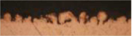
도 3은 본 발명의 방법으로 표면처리된 동박의 표면을 촬영한 이미지이다.
도 4는 본 발명의 방법으로 표면처리된 동박의 단면을 촬영한 이미지이다.
| 단계 | 구리 농도 | 황산 농도 | 전해액 온도 |
| 구리핵 생성 | 10 g/ℓ | 80 g/ℓ | 25 ℃ |
| 구리핵 성장 | 45 g/ℓ | 80 g/ℓ | 40 ℃ |
| 금속 종류 | 금속 농도 (g/ℓ) |
전류 밀도 (A/d㎡) |
도금시간 (sec) |
금속 전착량 (㎎/㎡) |
||
| 실시예 1 | 제1 금속 | Ni | 2 | 2.5 | 5 | 22.5 |
| 제2 금속 | Zn | 1 | 25.3 | |||
| 제3 금속 | Cr | 5 | 25.2 | |||
| 실시예 2 | 제1 금속 | Co | 2.5 | 2.5 | 5 | 18.7 |
| 제2 금속 | Zn | 1 | 20.3 | |||
| 제3 금속 | Cr | 5 | 27.3 | |||
| 실시예 3 | 제1 금속 | Ni | 2 | 2.5 | 5 | 25.3 |
| 제2 금속 | Sn | 1.5 | 27.8 | |||
| 제3 금속 | Cr | 5 | 22.3 | |||
| 실시예 4 | 제1 금속 | Ni | 2 | 2.5 | 5 | 20.7 |
| 제2 금속 | Zn | 1 | 23.5 | |||
| 제3 금속 | Mo | 3 | 27.3 | |||
| 실시예 5 | 제1 금속 | Ni | 1 | 2.5 | 5 | 13.5 |
| 제1 금속 | Co | 1.5 | 16.7 | |||
| 제2 금속 | Zn | 1 | 18.5 | |||
| 제3 금속 | Cr | 5 | 19.8 | |||
| 실시예 6 | 제1 금속 | W | 2 | 2.5 | 5 | 25.1 |
| 제2 금속 | Sn | 1.5 | 26.9 | |||
| 제3 금속 | Cr | 5 | 28.9 | |||
| 실시예 7 | 제1 금속 | Ni | 10 | 2.5 | 5 | 98.7 |
| 제2 금속 | Zn | 1 | 22.4 | |||
| 제3 금속 | Cr | 5 | 23.6 | |||
| 실시예 8 | 제1 금속 | Ni | 2 | 2.5 | 5 | 19.8 |
| 제2 금속 | Zn | 5 | 87.6 | |||
| 제3 금속 | Cr | 5 | 21.2 | |||
| 실시예 9 | 제1 금속 | Ni | 2 | 2.5 | 5 | 23.2 |
| 제2 금속 | Zn | 1 | 18.5 | |||
| 제3 금속 | Cr | 25 | 127.2 | |||
| 실시예 10 | 제1 금속 | Ni | 2 | 2.5 | 25 | 98.7 |
| 제2 금속 | Zn | 1 | 107.5 | |||
| 제3 금속 | Cr | 5 | 123.7 | |||
| 실시예 11 | 제1 금속 | Ni | 2 | 2.5 | 1.5 | 7.2 |
| 제2 금속 | Zn | 1 | 8.6 | |||
| 제3 금속 | Cr | 5 | 7.8 | |||
| 비교예 1 | 1차 처리 | Ni | 2 | 0.8 | 5 | 13.5 |
| 2차 처리 | Zn | 1 | 0.8 | 5 | 22.5 | |
| 3차 처리 | Cr | 5 | 0.8 | 5 | 26.4 | |
| 비교예 3 | 1차 처리 | Ni | 10 | 0.8 | 5 | 72.5 |
| 2차 처리 | Zn | 1 | 0.8 | 5 | 21.8 | |
| 3차 처리 | Cr | 5 | 0.8 | 5 | 24.7 | |
| 비교예 4 | 1차 처리 | Ni | 2 | 0.8 | 5 | 15.2 |
| 2차 처리 | Zn | 5 | 0.8 | 5 | 47.8 | |
| 3차 처리 | Cr | 5 | 0.8 | 5 | 25.3 | |
| 비교예 5 | 1차 처리 | Ni | 2 | 0.8 | 5 | 12.7 |
| 2차 처리 | Zn | 1 | 0.8 | 5 | 20.8 | |
| 3차 처리 | Cr | 25 | 0.8 | 5 | 107.8 | |
| 비교예 6 | 1차 처리 | Ni | 2 | 0.8 | 25 | 57.3 |
| 2차 처리 | Zn | 1 | 0.8 | 25 | 105.6 | |
| 3차 처리 | Cr | 5 | 0.8 | 25 | 112.5 | |
| 비교예 7 | 1차 처리 | Ni | 2 | 0.8 | 2 | 5.2 |
| 2차 처리 | Zn | 1 | 0.8 | 2 | 6.5 | |
| 3차 처리 | Cr | 5 | 0.8 | 2 | 7.1 | |
| 비교예 8 | 1차 처리 | Ni | 2 | 0.8 | 25 | 55.7 |
| 2차 처리 | Zn | 1 | 0.8 | 5 | 21.4 | |
| 3차 처리 | Cr | 5 | 0.8 | 5 | 27.3 | |
| 비교예 9 | 1차 처리 | Ni | 2 | 0.8 | 5 | 14.3 |
| 2차 처리 | Zn | 1 | 0.8 | 25 | 72.3 | |
| 3차 처리 | Cr | 5 | 0.8 | 5 | 25.4 | |
| 비교예 10 | 1차 처리 | Ni | 2 | 0.8 | 5 | 11.9 |
| 2차 처리 | Zn | 1 | 0.8 | 5 | 23.3 | |
| 3차 처리 | Cr | 5 | 0.8 | 25 | 98.7 | |
| * 상기 금속 농도는 금속 이온 자체의 농도임 | ||||||
| 접착강도A (kgf/㎝) |
접착강도B (kgf/㎝) |
내열성 (288℃,20초) |
내염산성(%) | |
| 실시예 1 | 4.48 | 4.32 | OK | 3% |
| 실시예 2 | 4.78 | 4.85 | OK | 3% |
| 실시예 3 | 5.02 | 4.88 | OK | 5% |
| 실시예 4 | 4.83 | 4.53 | OK | 2% |
| 실시예 5 | 4.85 | 4.65 | OK | 3% |
| 실시예 6 | 4.72 | 4.63 | OK | 1% |
| 실시예 7 | 4.69 | 4.55 | OK | 2.0% |
| 실시예 8 | 4.57 | 4.42 | OK | 1.3% |
| 실시예 9 | 4.59 | 4.43 | OK | 1.9% |
| 실시예 10 | 4.47 | 4.39 | OK | 5.1% |
| 실시예 11 | 4.53 | 4.48 | OK | 9.2% |
| 비교예 1 | 4.75 | 4.61 | OK | 3% |
| 비교예 2 | 3.89 | 1.93 | NG | 17% |
| 비교예 3 | 4.71 | 4.68 | OK | 1.1% |
| 비교예 4 | 4.45 | 4.28 | OK | 2.4% |
| 비교예 5 | 4.75 | 4.62 | OK | 1.3% |
| 비교예 6 | 4.54 | 4.47 | OK | 3.7% |
| 비교예 7 | 4.74 | 4.12 | OK | 11.1% |
| 비교예 8 | 4.65 | 4.49 | OK | 2.2% |
| 비교예 9 | 4.32 | 4.07 | OK | 1.1% |
| 비교예 10 | 4.57 | 4.32 | OK | 3.2% |
| 산화성 (180℃, 1hr) |
잔류 금속 테스트 | 손실율(%) | |
| 실시예 1 | OK | 잔류 없음 | 10 |
| 실시예 2 | OK | 잔류 없음 | 10 |
| 실시예 3 | OK | 잔류 없음 | 10 |
| 실시예 4 | OK | 미량 잔류 | 10 |
| 실시예 5 | OK | 잔류 없음 | 10 |
| 실시예 6 | OK | 미량 잔류 | 10 |
| 실시예 7 | OK | 미량 잔류 | 10 |
| 실시예 8 | OK | 잔류 없음 | 10 |
| 실시예 9 | OK | 미량 잔류 | 10 |
| 실시예 10 | OK | 미량 잔류 | 10 |
| 실시예 11 | OK | 잔류 없음 | 10 |
| 비교예 1 | OK | 잔류 없음 | 16 |
| 비교예 2 | NG | 잔류 없음 | 16 |
| 비교예 3 | OK | 다량 잔류 | 16 |
| 비교예 4 | OK | 미량 잔류 | 16 |
| 비교예 5 | OK | 다량 잔류 | 16 |
| 비교예 6 | OK | 다량 잔류 | 16 |
| 비교예 7 | OK | 잔류 없음 | 16 |
| 비교예 8 | OK | 다량 잔류 | 16 |
| 비교예 9 | OK | 미량 잔류 | 16 |
| 비교예 10 | OK | 다량 잔류 | 16 |
Claims (9)
- a) 동박의 표면에 노듈(nodule)을 형성시키는 단계;
b) 상기 노듈이 형성된 동박을 제1 금속, 제2 금속 및 제3 금속이 포함된 도금액에 투입하여 합금도금하는 단계; 및
c) 상기 합금도금된 동박에 실란 커플링제를 도포하는 단계를 포함하는 동박의 표면처리 방법. - 제1항에 있어서,
상기 제1 금속은 니켈(Ni), 코발트(Co), 니오브(Nb), 텅스텐(W), 구리(Cu), 아연(Zn) 및 몰리브덴(Mo)으로 이루어진 군에서 선택된 1종 이상 것을 특징으로 하는 동박의 표면처리 방법. - 제1항에 있어서,
상기 제2 금속은 아연(Zn) 또는 주석(Sn)인 것을 특징으로 하는 동박의 표면처리 방법. - 제1항에 있어서,
상기 제3 금속은 크롬(Cr) 또는 몰리브덴(Mo)인 것을 특징으로 하는 동박의 표면처리 방법. - 제1항에 있어서,
상기 도금액에 포함된 상기 제1 금속, 제2 금속 및 제3 금속의 농도비율은 0.5~3:0.5~3:2~7인 것을 특징으로 하는 동박의 표면처리 방법. - 제1항에 있어서,
상기 a) 단계는 노듈을 형성시키기 전에 동박의 표면을 세척하는 단계를 더 포함하는 것을 특징으로 하는 동박의 표면처리 방법. - 제1항 내지 제6항 중 어느 한 항의 방법으로 표면처리된 동박.
- 제7항에 있어서,
상기 동박은 압연 동박인 것을 특징으로 하는 표면처리된 동박. - 제7항의 동박을 포함하는 동박 적층체.
Priority Applications (4)
| Application Number | Priority Date | Filing Date | Title |
|---|---|---|---|
| PCT/KR2013/008195 WO2014042412A1 (ko) | 2012-09-12 | 2013-09-11 | 동박의 표면처리 방법 및 그 방법으로 표면처리된 동박 |
| US14/427,539 US20150245502A1 (en) | 2012-09-12 | 2013-09-11 | Method for surface-treating copper foil and copper foil surface-treated thereby |
| CN201380058610.0A CN104797744B (zh) | 2012-09-12 | 2013-09-11 | 铜箔的表面处理方法和由该方法进行了表面处理的铜箔 |
| EP13837186.9A EP2896723B1 (en) | 2012-09-12 | 2013-09-11 | Method for surface-treating copper foil and copper foil surface-treated thereby |
Applications Claiming Priority (2)
| Application Number | Priority Date | Filing Date | Title |
|---|---|---|---|
| KR1020120100953 | 2012-09-12 | ||
| KR20120100953 | 2012-09-12 |
Related Child Applications (1)
| Application Number | Title | Priority Date | Filing Date |
|---|---|---|---|
| KR1020160061810A Division KR101729440B1 (ko) | 2012-09-12 | 2016-05-20 | 동박의 표면처리 방법 및 그 방법으로 표면처리된 동박 |
Publications (1)
| Publication Number | Publication Date |
|---|---|
| KR20140034698A true KR20140034698A (ko) | 2014-03-20 |
Family
ID=50645059
Family Applications (2)
| Application Number | Title | Priority Date | Filing Date |
|---|---|---|---|
| KR1020130108233A Ceased KR20140034698A (ko) | 2012-09-12 | 2013-09-10 | 동박의 표면처리 방법 및 그 방법으로 표면처리된 동박 |
| KR1020160061810A Active KR101729440B1 (ko) | 2012-09-12 | 2016-05-20 | 동박의 표면처리 방법 및 그 방법으로 표면처리된 동박 |
Family Applications After (1)
| Application Number | Title | Priority Date | Filing Date |
|---|---|---|---|
| KR1020160061810A Active KR101729440B1 (ko) | 2012-09-12 | 2016-05-20 | 동박의 표면처리 방법 및 그 방법으로 표면처리된 동박 |
Country Status (5)
| Country | Link |
|---|---|
| US (1) | US20150245502A1 (ko) |
| EP (1) | EP2896723B1 (ko) |
| KR (2) | KR20140034698A (ko) |
| CN (1) | CN104797744B (ko) |
| WO (1) | WO2014042412A1 (ko) |
Cited By (3)
| Publication number | Priority date | Publication date | Assignee | Title |
|---|---|---|---|---|
| KR20170088602A (ko) | 2016-01-25 | 2017-08-02 | 엘에스엠트론 주식회사 | 전해 동박 및 그 제조 방법과, 동박적층판 및 인쇄회로기판 |
| CN110396684A (zh) * | 2018-10-31 | 2019-11-01 | 惠州联合铜箔电子材料有限公司 | 一种420-500微米超厚电解铜箔用工艺 |
| KR20200096419A (ko) * | 2019-02-01 | 2020-08-12 | 장 춘 페트로케미컬 컴퍼니 리미티드 | 전송 손실이 적은 인쇄 회로 기판용 전해 구리 호일 |
Families Citing this family (5)
| Publication number | Priority date | Publication date | Assignee | Title |
|---|---|---|---|---|
| US9647272B1 (en) | 2016-01-14 | 2017-05-09 | Chang Chun Petrochemical Co., Ltd. | Surface-treated copper foil |
| KR101734840B1 (ko) * | 2016-11-11 | 2017-05-15 | 일진머티리얼즈 주식회사 | 내굴곡성이 우수한 이차전지용 전해동박 및 그의 제조방법 |
| CN112779574B (zh) * | 2020-12-14 | 2023-09-15 | 安徽铜冠铜箔集团股份有限公司 | 一种增强电子铜箔导电性的电镀液、制备方法及电镀工艺 |
| US20250331107A1 (en) * | 2021-12-28 | 2025-10-23 | Shikoku Chemicals Corporation | Organic film and method for producing same |
| CN116970950B (zh) * | 2023-07-13 | 2024-11-08 | 南通麦特隆新材料科技有限公司 | 一种pet铜箔及其制备方法 |
Family Cites Families (14)
| Publication number | Priority date | Publication date | Assignee | Title |
|---|---|---|---|---|
| US5338619A (en) * | 1991-05-16 | 1994-08-16 | Fukuda Metal Foil And Powder Co., Ltd. | Copper foil for printed circuits and method of producing same |
| JP3067672B2 (ja) * | 1997-02-13 | 2000-07-17 | 日本電解株式会社 | プリント配線板用銅箔及びその製造方法 |
| US6610417B2 (en) * | 2001-10-04 | 2003-08-26 | Oak-Mitsui, Inc. | Nickel coated copper as electrodes for embedded passive devices |
| KR100401340B1 (ko) * | 2001-11-16 | 2003-10-10 | 엘지전선 주식회사 | Pcb용 전해동박의 표면처리방법 |
| KR100559933B1 (ko) * | 2002-11-29 | 2006-03-13 | 엘에스전선 주식회사 | 저조도 동박의 전해연마방법 및 전해연마장치와 동박 |
| TW200424359A (en) * | 2003-02-04 | 2004-11-16 | Furukawa Circuit Foil | Copper foil for high frequency circuit, method of production and apparatus for production of same, and high frequency circuit using copper foil |
| TW200500199A (en) * | 2003-02-12 | 2005-01-01 | Furukawa Circuit Foil | Copper foil for fine patterned printed circuits and method of production of same |
| KR100654737B1 (ko) * | 2004-07-16 | 2006-12-08 | 일진소재산업주식회사 | 미세회로기판용 표면처리동박의 제조방법 및 그 동박 |
| JP4904933B2 (ja) * | 2005-09-27 | 2012-03-28 | 日立電線株式会社 | ニッケルめっき液とその製造方法、ニッケルめっき方法およびプリント配線板用銅箔 |
| JP2008179127A (ja) * | 2007-01-15 | 2008-08-07 | Ls Cable Ltd | 銅箔積層構造体及び銅箔の表面処理方法 |
| KR100953464B1 (ko) * | 2007-01-15 | 2010-04-16 | 엘에스엠트론 주식회사 | 동박 적층 구조체 및 동박 표면 처리 방법 |
| KR100857311B1 (ko) * | 2007-06-18 | 2008-09-05 | 엘에스엠트론 주식회사 | 전해동박 및 그의 표면처리방법 |
| KR100991756B1 (ko) * | 2007-12-17 | 2010-11-03 | (주)인터플렉스 | 양면 연성인쇄회로기판의 제조방법 |
| KR100983682B1 (ko) * | 2008-03-31 | 2010-09-24 | 엘에스엠트론 주식회사 | 인쇄회로용 동박의 표면처리 방법과 그에 따라 제조된 동박및 그 도금장치 |
-
2013
- 2013-09-10 KR KR1020130108233A patent/KR20140034698A/ko not_active Ceased
- 2013-09-11 WO PCT/KR2013/008195 patent/WO2014042412A1/ko not_active Ceased
- 2013-09-11 EP EP13837186.9A patent/EP2896723B1/en not_active Not-in-force
- 2013-09-11 CN CN201380058610.0A patent/CN104797744B/zh not_active Expired - Fee Related
- 2013-09-11 US US14/427,539 patent/US20150245502A1/en not_active Abandoned
-
2016
- 2016-05-20 KR KR1020160061810A patent/KR101729440B1/ko active Active
Cited By (4)
| Publication number | Priority date | Publication date | Assignee | Title |
|---|---|---|---|---|
| KR20170088602A (ko) | 2016-01-25 | 2017-08-02 | 엘에스엠트론 주식회사 | 전해 동박 및 그 제조 방법과, 동박적층판 및 인쇄회로기판 |
| CN110396684A (zh) * | 2018-10-31 | 2019-11-01 | 惠州联合铜箔电子材料有限公司 | 一种420-500微米超厚电解铜箔用工艺 |
| CN110396684B (zh) * | 2018-10-31 | 2020-08-28 | 惠州联合铜箔电子材料有限公司 | 一种420-500微米超厚电解铜箔用工艺 |
| KR20200096419A (ko) * | 2019-02-01 | 2020-08-12 | 장 춘 페트로케미컬 컴퍼니 리미티드 | 전송 손실이 적은 인쇄 회로 기판용 전해 구리 호일 |
Also Published As
| Publication number | Publication date |
|---|---|
| KR20160064054A (ko) | 2016-06-07 |
| US20150245502A1 (en) | 2015-08-27 |
| CN104797744B (zh) | 2018-08-07 |
| EP2896723A1 (en) | 2015-07-22 |
| EP2896723B1 (en) | 2017-08-09 |
| WO2014042412A1 (ko) | 2014-03-20 |
| EP2896723A4 (en) | 2016-06-15 |
| CN104797744A (zh) | 2015-07-22 |
| KR101729440B1 (ko) | 2017-05-02 |
Similar Documents
| Publication | Publication Date | Title |
|---|---|---|
| CN111519215B (zh) | 用于印刷电路板的具有低传输损耗的电解铜箔 | |
| KR101729440B1 (ko) | 동박의 표면처리 방법 및 그 방법으로 표면처리된 동박 | |
| EP2100987B1 (en) | Surface treated copper foil, surface treated copper foil with very thin primer resin layer, method for manufacturing the surface treated copper foil, and method for manufacturing the surface treated copper foil with very thin primer resin layer | |
| CN106011965B (zh) | 一种电解铜箔表面的微细粗化处理工艺 | |
| DE102007045794A1 (de) | Haftvermittler für Harz und Verfahren zur Erzeugung eines Laminates, umfassend den Haftvermittler | |
| JP3250994B2 (ja) | 電解銅箔 | |
| KR20150126008A (ko) | 캐리어 부착 동박, 그것을 사용한 구리 피복 적층판, 프린트 배선판, 전자 기기 및 프린트 배선판의 제조 방법 | |
| JP5406905B2 (ja) | 高剥離強度と環境にやさしい微細な粒状表面からなるプリント回路基板用銅箔の製造方法。 | |
| CN102711393B (zh) | 一种印刷电路基板用表面细晶粒铜箔的制造方法 | |
| KR100654737B1 (ko) | 미세회로기판용 표면처리동박의 제조방법 및 그 동박 | |
| EP2590487B1 (en) | Process to manufacture fine grain surface copper foil with high peeling strength and environmental protection for printed circuit boards | |
| US7344785B2 (en) | Copper foil for printed circuit board, method for fabricating same, and trivalent chromium conversion treatment solution used for fabricating same | |
| JP3623621B2 (ja) | 銅箔の表面処理方法 | |
| KR101096638B1 (ko) | 구리 라미네이트의 박리 강도 강화 | |
| JP2631061B2 (ja) | プリント回路用銅箔及びその製造方法 | |
| US9115441B2 (en) | Process to manufacture surface fine grain copper foil with high peeling strength and environmental protection for printed circuit boards | |
| TWI415742B (zh) | A method for manufacturing fine grain copper foil with high peel strength and environmental protection for printed circuit board tool | |
| CN107018622A (zh) | 微电路基板用经表面处理的铜箔及其制造方法 | |
| JPH0314915B2 (ko) | ||
| KR102504286B1 (ko) | 표면 처리 동박 및 그 제조방법 | |
| JP2005340635A (ja) | プリント配線板用圧延銅箔及びその製造方法 | |
| JP3806677B2 (ja) | プリント配線板用銅箔 | |
| JP2008297569A (ja) | 表面処理銅箔 | |
| JPH0376798B2 (ko) | ||
| JP2005353920A (ja) | プリント配線板用銅箔の表面粗化処理方法 |
Legal Events
| Date | Code | Title | Description |
|---|---|---|---|
| A201 | Request for examination | ||
| PA0109 | Patent application |
Patent event code: PA01091R01D Comment text: Patent Application Patent event date: 20130910 |
|
| PA0201 | Request for examination | ||
| PG1501 | Laying open of application | ||
| E902 | Notification of reason for refusal | ||
| PE0902 | Notice of grounds for rejection |
Comment text: Notification of reason for refusal Patent event date: 20140808 Patent event code: PE09021S01D |
|
| AMND | Amendment | ||
| E601 | Decision to refuse application | ||
| PE0601 | Decision on rejection of patent |
Patent event date: 20150520 Comment text: Decision to Refuse Application Patent event code: PE06012S01D Patent event date: 20140808 Comment text: Notification of reason for refusal Patent event code: PE06011S01I |
|
| X091 | Application refused [patent] | ||
| AMND | Amendment | ||
| PX0901 | Re-examination |
Patent event code: PX09011S01I Patent event date: 20150520 Comment text: Decision to Refuse Application Patent event code: PX09012R01I Patent event date: 20150106 Comment text: Amendment to Specification, etc. |
|
| E902 | Notification of reason for refusal | ||
| PE0902 | Notice of grounds for rejection |
Comment text: Notification of reason for refusal Patent event date: 20150804 Patent event code: PE09021S01D |
|
| AMND | Amendment | ||
| PX0601 | Decision of rejection after re-examination |
Comment text: Decision to Refuse Application Patent event code: PX06014S01D Patent event date: 20160421 Comment text: Amendment to Specification, etc. Patent event code: PX06012R01I Patent event date: 20160202 Comment text: Notification of reason for refusal Patent event code: PX06013S01I Patent event date: 20150804 Comment text: Amendment to Specification, etc. Patent event code: PX06012R01I Patent event date: 20150715 Comment text: Decision to Refuse Application Patent event code: PX06011S01I Patent event date: 20150520 Comment text: Amendment to Specification, etc. Patent event code: PX06012R01I Patent event date: 20150106 Comment text: Notification of reason for refusal Patent event code: PX06013S01I Patent event date: 20140808 |
|
| X601 | Decision of rejection after re-examination | ||
| A107 | Divisional application of patent | ||
| PA0107 | Divisional application |
Comment text: Divisional Application of Patent Patent event date: 20160520 Patent event code: PA01071R01D |