KR20140048083A - 터치 디스플레이 패널 - Google Patents
터치 디스플레이 패널 Download PDFInfo
- Publication number
- KR20140048083A KR20140048083A KR1020137022555A KR20137022555A KR20140048083A KR 20140048083 A KR20140048083 A KR 20140048083A KR 1020137022555 A KR1020137022555 A KR 1020137022555A KR 20137022555 A KR20137022555 A KR 20137022555A KR 20140048083 A KR20140048083 A KR 20140048083A
- Authority
- KR
- South Korea
- Prior art keywords
- comb
- line
- detection line
- common electrode
- pixel electrode
- Prior art date
- Legal status (The legal status is an assumption and is not a legal conclusion. Google has not performed a legal analysis and makes no representation as to the accuracy of the status listed.)
- Granted
Links
Images








Classifications
-
- G—PHYSICS
- G06—COMPUTING OR CALCULATING; COUNTING
- G06F—ELECTRIC DIGITAL DATA PROCESSING
- G06F3/00—Input arrangements for transferring data to be processed into a form capable of being handled by the computer; Output arrangements for transferring data from processing unit to output unit, e.g. interface arrangements
- G06F3/01—Input arrangements or combined input and output arrangements for interaction between user and computer
- G06F3/03—Arrangements for converting the position or the displacement of a member into a coded form
- G06F3/041—Digitisers, e.g. for touch screens or touch pads, characterised by the transducing means
- G06F3/0412—Digitisers structurally integrated in a display
-
- G—PHYSICS
- G02—OPTICS
- G02F—OPTICAL DEVICES OR ARRANGEMENTS FOR THE CONTROL OF LIGHT BY MODIFICATION OF THE OPTICAL PROPERTIES OF THE MEDIA OF THE ELEMENTS INVOLVED THEREIN; NON-LINEAR OPTICS; FREQUENCY-CHANGING OF LIGHT; OPTICAL LOGIC ELEMENTS; OPTICAL ANALOGUE/DIGITAL CONVERTERS
- G02F1/00—Devices or arrangements for the control of the intensity, colour, phase, polarisation or direction of light arriving from an independent light source, e.g. switching, gating or modulating; Non-linear optics
- G02F1/01—Devices or arrangements for the control of the intensity, colour, phase, polarisation or direction of light arriving from an independent light source, e.g. switching, gating or modulating; Non-linear optics for the control of the intensity, phase, polarisation or colour
- G02F1/13—Devices or arrangements for the control of the intensity, colour, phase, polarisation or direction of light arriving from an independent light source, e.g. switching, gating or modulating; Non-linear optics for the control of the intensity, phase, polarisation or colour based on liquid crystals, e.g. single liquid crystal display cells
- G02F1/133—Constructional arrangements; Operation of liquid crystal cells; Circuit arrangements
- G02F1/1333—Constructional arrangements; Manufacturing methods
- G02F1/13338—Input devices, e.g. touch panels
-
- G—PHYSICS
- G06—COMPUTING OR CALCULATING; COUNTING
- G06F—ELECTRIC DIGITAL DATA PROCESSING
- G06F3/00—Input arrangements for transferring data to be processed into a form capable of being handled by the computer; Output arrangements for transferring data from processing unit to output unit, e.g. interface arrangements
- G06F3/01—Input arrangements or combined input and output arrangements for interaction between user and computer
- G06F3/03—Arrangements for converting the position or the displacement of a member into a coded form
- G06F3/041—Digitisers, e.g. for touch screens or touch pads, characterised by the transducing means
- G06F3/044—Digitisers, e.g. for touch screens or touch pads, characterised by the transducing means by capacitive means
- G06F3/0443—Digitisers, e.g. for touch screens or touch pads, characterised by the transducing means by capacitive means using a single layer of sensing electrodes
-
- G—PHYSICS
- G06—COMPUTING OR CALCULATING; COUNTING
- G06F—ELECTRIC DIGITAL DATA PROCESSING
- G06F3/00—Input arrangements for transferring data to be processed into a form capable of being handled by the computer; Output arrangements for transferring data from processing unit to output unit, e.g. interface arrangements
- G06F3/01—Input arrangements or combined input and output arrangements for interaction between user and computer
- G06F3/03—Arrangements for converting the position or the displacement of a member into a coded form
- G06F3/041—Digitisers, e.g. for touch screens or touch pads, characterised by the transducing means
- G06F3/044—Digitisers, e.g. for touch screens or touch pads, characterised by the transducing means by capacitive means
- G06F3/0445—Digitisers, e.g. for touch screens or touch pads, characterised by the transducing means by capacitive means using two or more layers of sensing electrodes, e.g. using two layers of electrodes separated by a dielectric layer
-
- G—PHYSICS
- G06—COMPUTING OR CALCULATING; COUNTING
- G06F—ELECTRIC DIGITAL DATA PROCESSING
- G06F3/00—Input arrangements for transferring data to be processed into a form capable of being handled by the computer; Output arrangements for transferring data from processing unit to output unit, e.g. interface arrangements
- G06F3/01—Input arrangements or combined input and output arrangements for interaction between user and computer
- G06F3/03—Arrangements for converting the position or the displacement of a member into a coded form
- G06F3/041—Digitisers, e.g. for touch screens or touch pads, characterised by the transducing means
- G06F3/044—Digitisers, e.g. for touch screens or touch pads, characterised by the transducing means by capacitive means
- G06F3/0446—Digitisers, e.g. for touch screens or touch pads, characterised by the transducing means by capacitive means using a grid-like structure of electrodes in at least two directions, e.g. using row and column electrodes
-
- G—PHYSICS
- G06—COMPUTING OR CALCULATING; COUNTING
- G06F—ELECTRIC DIGITAL DATA PROCESSING
- G06F3/00—Input arrangements for transferring data to be processed into a form capable of being handled by the computer; Output arrangements for transferring data from processing unit to output unit, e.g. interface arrangements
- G06F3/01—Input arrangements or combined input and output arrangements for interaction between user and computer
- G06F3/03—Arrangements for converting the position or the displacement of a member into a coded form
- G06F3/041—Digitisers, e.g. for touch screens or touch pads, characterised by the transducing means
- G06F3/044—Digitisers, e.g. for touch screens or touch pads, characterised by the transducing means by capacitive means
- G06F3/0448—Details of the electrode shape, e.g. for enhancing the detection of touches, for generating specific electric field shapes, for enhancing display quality
-
- G—PHYSICS
- G02—OPTICS
- G02F—OPTICAL DEVICES OR ARRANGEMENTS FOR THE CONTROL OF LIGHT BY MODIFICATION OF THE OPTICAL PROPERTIES OF THE MEDIA OF THE ELEMENTS INVOLVED THEREIN; NON-LINEAR OPTICS; FREQUENCY-CHANGING OF LIGHT; OPTICAL LOGIC ELEMENTS; OPTICAL ANALOGUE/DIGITAL CONVERTERS
- G02F1/00—Devices or arrangements for the control of the intensity, colour, phase, polarisation or direction of light arriving from an independent light source, e.g. switching, gating or modulating; Non-linear optics
- G02F1/01—Devices or arrangements for the control of the intensity, colour, phase, polarisation or direction of light arriving from an independent light source, e.g. switching, gating or modulating; Non-linear optics for the control of the intensity, phase, polarisation or colour
- G02F1/13—Devices or arrangements for the control of the intensity, colour, phase, polarisation or direction of light arriving from an independent light source, e.g. switching, gating or modulating; Non-linear optics for the control of the intensity, phase, polarisation or colour based on liquid crystals, e.g. single liquid crystal display cells
- G02F1/133—Constructional arrangements; Operation of liquid crystal cells; Circuit arrangements
- G02F1/1333—Constructional arrangements; Manufacturing methods
- G02F1/1343—Electrodes
- G02F1/134309—Electrodes characterised by their geometrical arrangement
- G02F1/134318—Electrodes characterised by their geometrical arrangement having a patterned common electrode
Landscapes
- Engineering & Computer Science (AREA)
- General Engineering & Computer Science (AREA)
- Theoretical Computer Science (AREA)
- Physics & Mathematics (AREA)
- General Physics & Mathematics (AREA)
- Human Computer Interaction (AREA)
- Quality & Reliability (AREA)
- Nonlinear Science (AREA)
- Liquid Crystal (AREA)
- Mathematical Physics (AREA)
- Chemical & Material Sciences (AREA)
- Crystallography & Structural Chemistry (AREA)
- Optics & Photonics (AREA)
Abstract
Description
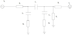
도 2는 도 1의 등가 회로도이며,
도 3은 종래 기술에서 용량성 터치 디스플레이 패널의 접촉층이 접촉된 경우의 구조도이며,
도 4는 도 3의 등가 회로도이며,
도 5는 본 발명에 따른 터치 디스플레이 패널의 구조도이며,
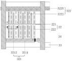
도 6은 IPS-LCD 터치 디스플레이 패널의 제1 종의 TFT 기판의 화소 유닛의 평면도이며,
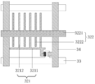
도 7은 도 6의 I-I 선을 따라 취한 단면도이며,
도 8은 도 7의 구조에 대한 최적화 구조의 구조 단면도이며,
도 9는 본 발명에 따른 구동 라인의 구조도이며,
도 10은 본 발명에 따른 검출 라인의 구조도이며,
도 11은 도 6에서 CF 기판과 TFT 기판의 화소 유닛에 의해 형성된 터치 패널의 평면도이며,
도 12는 도 11의 II-II 선을 따라 취한 단면도이며,
도 13 은 IPS-LCD 터치 디스플레이 패널의 제2 종의 TFT 기판의 화소 유닛의 평면도이며,
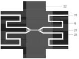
도 14는 본 발명에 다른 접촉층의 구조도이며,
도 15는 도 14의 영역(Q)의 확대도이며,
도 16은 IPS-LCD 터치 디스플레이 패널의 제2 종의 TFT 기판의 단면도이며,
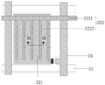
도 17은 FFS-LCD 터치 디스플레이 패널의 TFT 기판의 화소 유닛의 평면도이며,
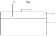
도 18은 도 17의 III-III 선을 따라 취한 단면도이며,
도 19는 도 18의 구조에 대한 최적화 구조의 구조 단면도이며,
도 20은 도 17에서 CF 기판과 TFT 기판의 화소 유닛에 의해 형성된 터치 패널의 평면도이며,
도 21은 도 20의 IV-IV 선을 따라 취한 단면도이다.
구동 라인(11) 검출 라인(12)
CF 기판(2) TFT 기판(3)
액정층(4) 유리 기판(31)
전극층(32) 게이트 라인(33)
데이터 라인(34) 화소 전극(321)
화소 전극 막대 형상부(3211) 화소 전극 빗 형상부(3212)
공통 전극(322) 공통 전극 막대 형상부(3221)
공통 전극 빗 형상부(3222) 보호 필름(35)
정렬층(36) 구동 라인(22)
검출 라인(24) 구동 라인 막대 형상부(221)
구동 라인 빗 형상부(222) 검출 라인 막대 형상부(241)
검출 라인 빗 형상부(242) 보호층(37)
절연층(38) 유전층(23)
유리 기판(21)
Claims (14)
- 서로 대향 배치된 컬러 필름(CF) 기판과 박막 트랜지스터(TFT) 기판, 상기 CF 기판과 TFT 기판 사이에 배치된 액정층을 구비하며, 빗 형상 구조를 가진 공통 전극 및/또는 빗 형상 구조를 가진 화소 전극이 상기 액정층에 인접한 TFT 기판 상에 배치되어 있고, 접촉층이 액정층에 인접한 CF 기판 상에 배치되어 있고, 상기 접촉층은 서로 절연되어 있는 구동 라인과 검출 라인을 포함하고, 상기 구동 라인 및/또는 상기 검출 라인은 상기 공통 전극의 빗 형상 구조 및/또는 상기 화소 전극의 빗 형상 구조에 대해 적어도 부분적으로 오정렬되어 있는 빗 형상 구조를 가지는 것인 터치 디스플레이 패널.
- 제1항에 있어서, 상기 구동 라인의 빗 형상 구조 및/또는 상기 검출 라인의 빗 형상 구조는 상기 공통 전극의 빗 형상 구조 및/또는 상기 화소 전극의 빗 형상 구조에 상보적인 것인 터치 디스플레이 패널.
- 제1항에 있어서, 상기 구동 라인 및 상기 검출 라인은 동일한 층에 형성되고, 상기 구동 라인은 상기 검출 라인에 수직인 것인 터치 디스플레이 패널.
- 제3항에 있어서, 상기 검출 라인은 상기 구동 라인에 의해 다수의 분리부로 분리되고, 제1 연결부는 상기 분리부 상에 배치되고, 상기 제1 연결부는 상기 구동 라인을 교차시켜 상기 검출 라인의 분리부를 연결시키는 것인 터치 디스플레이 패널.
- 제3항에 있어서, 상기 구동 라인은 상기 검출 라인에 의해 다수의 분리부로 분리되고, 제2 연결부는 상기 분리부 상에 배치되고, 상기 제2 연결부는 상기 검출 라인을 교차시켜 상기 구동 라인의 분리부를 연결시키는 것인 터치 디스플레이 패널.
- 제1항에 있어서, 상기 접촉층은 서로 절연되어 있는 제1 접촉층 및 제2 접촉층을 포함하고, 상기 구동 라인은 제1 접촉층에 형성되고, 상기 검출 라인은 제2 접촉층에 형성되는 것인 터치 디스플레이 패널.
- 제6항에 있어서, 상기 제2 접촉층은 상기 제1 접촉층보다 상기 액정층에 더 가깝고, 상기 검출 라인은 상기 공통 전극의 빗 형상 구조 및/또는 상기 화소 전극의 빗 형상 구조에 대해 오정렬되어 있는 빗 형상 구조를 가지는 것인 터치 디스플레이 패널.
- 제6항에 있어서, 상기 제1 접촉층은 상기 제2 접촉층보다 상기 액정층에 더 가깝고, 상기 구동 라인은 상기 공통 전극의 빗 형상 구조 및/또는 상기 화소 전극의 빗 형상 구조에 대해 오정렬되어 있는 빗 형상 구조를 가지는 것인 터치 디스플레이 패널.
- 제1항에 있어서, 상기 공통 전극은 상기 액정층에 인접한 TFT 기판의 표면에 배치되고, 상기 공통 전극은 빗 형상 구조를 가지고, 상기 구동 라인 및/또는 상기 검출 라인의 빗 형상 구조는 상기 공통 전극의 빗 형상 구조에 대해 적어도 부분적으로 오정렬되어 있는 것인 터치 디스플레이 패널.
- 제1항에 있어서, 상기 화소 전극은 상기 액정층에 인접한 TFT 기판의 표면에 배치되고, 상기 화소 전극은 빗 형상 구조를 가지고, 상기 구동 라인 및/또는 상기 검출 라인의 빗 형상 구조는 상기 화소 전극의 빗 형상 구조에 대해 적어도 부분적으로 오정렬되어 있는 것인 터치 디스플레이 패널.
- 제1항에 있어서, 상기 공통 전극 및 상기 화소 전극은 상기 액정층에 인접한 TFT 기판의 표면에 배치되고, 상기 공통 전극 및 상기 화소 전극은 서로에 대해 분리된 빗 형상 구조를 가지고, 상기 구동 라인 및/또는 상기 검출 라인의 빗 형상 구조는 상기 공통 전극의 빗 형상 구조와 상기 화소 전극의 빗 형상 구조 양자에 대해 적어도 부분적으로 오정렬되어 있는 것인 터치 디스플레이 패널.
- 제1항에 있어서, 상기 구동 라인 및 상기 검출 라인의 재료는 투명한 것인 터치 디스플레이 패널.
- 제1항에 있어서, 상기 공통 전극 또는 상기 화소 전극의 재료는 투명한 것인 터치 디스플레이 패널.
- 제12항에 있어서, 상기 구동 라인 및 상기 검출 라인의 재료는 산화 인듐 주석, 산화 인듐 아연, 또는 이의 조합물인 것인 터치 디스플레이 패널.
Applications Claiming Priority (3)
| Application Number | Priority Date | Filing Date | Title |
|---|---|---|---|
| CN201210253996.8A CN103294246B (zh) | 2012-07-20 | 2012-07-20 | 触摸显示面板 |
| CN201210253996.8 | 2012-07-20 | ||
| PCT/CN2012/085946 WO2014012319A1 (zh) | 2012-07-20 | 2012-12-05 | 触摸显示面板 |
Publications (2)
| Publication Number | Publication Date |
|---|---|
| KR20140048083A true KR20140048083A (ko) | 2014-04-23 |
| KR101534425B1 KR101534425B1 (ko) | 2015-07-06 |
Family
ID=49095254
Family Applications (1)
| Application Number | Title | Priority Date | Filing Date |
|---|---|---|---|
| KR1020137022555A Expired - Fee Related KR101534425B1 (ko) | 2012-07-20 | 2012-12-05 | 터치 디스플레이 패널 |
Country Status (5)
| Country | Link |
|---|---|
| US (1) | US9588368B2 (ko) |
| EP (1) | EP2706442B1 (ko) |
| KR (1) | KR101534425B1 (ko) |
| CN (1) | CN103294246B (ko) |
| WO (1) | WO2014012319A1 (ko) |
Cited By (2)
| Publication number | Priority date | Publication date | Assignee | Title |
|---|---|---|---|---|
| KR20160043585A (ko) * | 2014-10-13 | 2016-04-22 | 삼성디스플레이 주식회사 | 터치 스크린 패널 |
| KR20210032946A (ko) * | 2014-10-13 | 2021-03-25 | 삼성디스플레이 주식회사 | 터치 스크린 패널 |
Families Citing this family (20)
| Publication number | Priority date | Publication date | Assignee | Title |
|---|---|---|---|---|
| US9645431B2 (en) * | 2008-03-19 | 2017-05-09 | Egalax_Empia Technology Inc. | Touch display and method for driving a plurality of touch driving electrodes of touch display |
| KR102128394B1 (ko) * | 2013-09-11 | 2020-07-01 | 삼성디스플레이 주식회사 | 터치 감지 표시 장치 |
| CN103529607B (zh) | 2013-10-29 | 2017-05-31 | 京东方科技集团股份有限公司 | 一种液晶显示面板、显示装置及其驱动方法 |
| CN103955309B (zh) * | 2014-04-14 | 2017-08-25 | 京东方科技集团股份有限公司 | 显示面板及其驱动方法、显示装置 |
| CN103995617B (zh) * | 2014-05-30 | 2018-09-07 | 京东方科技集团股份有限公司 | 内嵌式触控显示面板、其操作方法及显示装置 |
| US20160034063A1 (en) * | 2014-07-29 | 2016-02-04 | Hannstar Display (Nanjing) Corporation | Anti-interference touch display panel |
| CN104503648B (zh) * | 2015-01-09 | 2017-06-09 | 京东方科技集团股份有限公司 | 一种内嵌式触摸屏及显示装置 |
| CN105094422B (zh) * | 2015-06-23 | 2018-09-11 | 京东方科技集团股份有限公司 | 一种触控显示面板、其制备方法、驱动方法及显示装置 |
| CN105093736A (zh) * | 2015-07-14 | 2015-11-25 | 京东方科技集团股份有限公司 | Ips阵列基板及其制作方法、显示器件 |
| CN105826328B (zh) * | 2016-05-03 | 2019-03-05 | 京东方科技集团股份有限公司 | 阵列基板及其制造方法、显示装置 |
| WO2017195339A1 (ja) * | 2016-05-13 | 2017-11-16 | 凸版印刷株式会社 | 表示装置 |
| TWI596527B (zh) * | 2016-12-14 | 2017-08-21 | 友達光電股份有限公司 | 觸控顯示裝置 |
| CN109557728B (zh) * | 2017-09-25 | 2021-12-10 | 京东方科技集团股份有限公司 | 像素结构及其制作方法、阵列基板和触控显示装置 |
| TWI654548B (zh) * | 2017-10-27 | 2019-03-21 | 友達光電股份有限公司 | 觸控裝置 |
| CN207601768U (zh) * | 2017-11-30 | 2018-07-10 | 昆山国显光电有限公司 | 一种触控面板及触控显示装置 |
| CN108803945B (zh) * | 2018-09-05 | 2024-04-12 | 京东方科技集团股份有限公司 | 一种触摸屏及显示设备 |
| KR102856005B1 (ko) | 2019-10-30 | 2025-09-05 | 엘지디스플레이 주식회사 | 터치 디스플레이 장치 및 디스플레이 패널 |
| CN111540713B (zh) * | 2020-05-09 | 2022-07-26 | 青岛三顺智能电器有限公司 | 一种触摸显示面板及其制造方法 |
| CN114698267B (zh) * | 2021-08-09 | 2024-06-04 | 上海航天电子通讯设备研究所 | Lcp多层柔性电路板曲面成型方法 |
| KR20250035693A (ko) * | 2023-09-05 | 2025-03-13 | 삼성디스플레이 주식회사 | 터치 패널 및 이를 포함하는 표시 장치 |
Family Cites Families (12)
| Publication number | Priority date | Publication date | Assignee | Title |
|---|---|---|---|---|
| JP3444540B2 (ja) * | 2000-10-17 | 2003-09-08 | 松下電器産業株式会社 | アクティブマトリックス型液晶表示装置 |
| JP3774858B2 (ja) * | 2001-04-07 | 2006-05-17 | 大林精工株式会社 | 液晶表示装置とその駆動方法 |
| CN104965621B (zh) * | 2006-06-09 | 2018-06-12 | 苹果公司 | 触摸屏液晶显示器及其操作方法 |
| JP4916852B2 (ja) * | 2006-11-29 | 2012-04-18 | 株式会社 日立ディスプレイズ | タッチパネル付き液晶表示装置 |
| CN101556390B (zh) * | 2008-04-09 | 2012-07-18 | 北京京东方光电科技有限公司 | 用于三维显示装置的开关面板和液晶显示系统 |
| JP2009265512A (ja) * | 2008-04-28 | 2009-11-12 | Sony Corp | 液晶表示装置 |
| JP5206250B2 (ja) * | 2008-05-02 | 2013-06-12 | セイコーエプソン株式会社 | 表示装置および電子機器 |
| TWI497157B (zh) * | 2009-06-19 | 2015-08-21 | Tpk Touch Solutions Inc | 具觸控功能的平面轉換式液晶顯示器 |
| CN101930132A (zh) * | 2009-06-22 | 2010-12-29 | 上海天马微电子有限公司 | 集成触摸屏及集成触摸屏的检测方法 |
| KR20120017587A (ko) * | 2010-08-19 | 2012-02-29 | 삼성모바일디스플레이주식회사 | 터치스크린패널 일체형 액정표시장치 |
| TW201227454A (en) * | 2010-12-31 | 2012-07-01 | Hong-Da Liu | An active array having the touchable sensing matrix unit and a display having the active array |
| JP5789113B2 (ja) * | 2011-03-31 | 2015-10-07 | 株式会社Joled | 表示装置および電子機器 |
-
2012
- 2012-07-20 CN CN201210253996.8A patent/CN103294246B/zh not_active Expired - Fee Related
- 2012-12-05 WO PCT/CN2012/085946 patent/WO2014012319A1/zh not_active Ceased
- 2012-12-05 KR KR1020137022555A patent/KR101534425B1/ko not_active Expired - Fee Related
- 2012-12-05 EP EP12868921.3A patent/EP2706442B1/en not_active Not-in-force
-
2013
- 2013-08-30 US US14/014,948 patent/US9588368B2/en not_active Expired - Fee Related
Cited By (2)
| Publication number | Priority date | Publication date | Assignee | Title |
|---|---|---|---|---|
| KR20160043585A (ko) * | 2014-10-13 | 2016-04-22 | 삼성디스플레이 주식회사 | 터치 스크린 패널 |
| KR20210032946A (ko) * | 2014-10-13 | 2021-03-25 | 삼성디스플레이 주식회사 | 터치 스크린 패널 |
Also Published As
| Publication number | Publication date |
|---|---|
| KR101534425B1 (ko) | 2015-07-06 |
| CN103294246B (zh) | 2016-03-16 |
| WO2014012319A1 (zh) | 2014-01-23 |
| EP2706442B1 (en) | 2022-04-27 |
| EP2706442A1 (en) | 2014-03-12 |
| US9588368B2 (en) | 2017-03-07 |
| US20140022210A1 (en) | 2014-01-23 |
| CN103294246A (zh) | 2013-09-11 |
| EP2706442A4 (en) | 2015-07-08 |
Similar Documents
| Publication | Publication Date | Title |
|---|---|---|
| KR101534425B1 (ko) | 터치 디스플레이 패널 | |
| CN103164076B (zh) | 具有集成式触摸屏的显示装置 | |
| CN114647340B (zh) | 集成触摸屏 | |
| US8687135B2 (en) | Stereoscopic liquid crystal display device having touch panel and method for manufacturing the same | |
| US9645665B2 (en) | In-cell touch panel and display device | |
| US9449992B2 (en) | Display apparatus having touch sensing part and method of manufacturing the same | |
| KR102468767B1 (ko) | 터치 일체형 표시패널 | |
| JP5971708B2 (ja) | タッチパネル内蔵型表示装置 | |
| TWI537635B (zh) | 整合型觸控螢幕 | |
| US8300027B2 (en) | Vibration touch sensor, method for vibration touch sensing and vibration touch screen display panel | |
| KR101360782B1 (ko) | 터치 스크린 일체형 표시장치 | |
| EP2527912B1 (en) | Liquid crystal display panel and driving method thereof | |
| KR20140061314A (ko) | 터치 센서, 내장형 터치 액정 디스플레이 패널 및 액정 디스플레이 | |
| JP2008009750A (ja) | タッチパネル付き液晶表示素子 | |
| CN103186297B (zh) | 一种电容式触摸液晶显示面板和液晶显示装置 | |
| CN103049155A (zh) | 一种内嵌式触摸屏及显示装置 | |
| EP2804043A1 (en) | Array substrate, touch liquid crystal display panel and manufacturing method thereof | |
| JP2009186869A (ja) | 液晶表示装置 | |
| US20160377898A1 (en) | Ips in-cell touch display panel and manufacturing method thereof | |
| KR20160081039A (ko) | 인셀 터치 방식을 이용한 액정표시장치 및 그 제조방법 | |
| CN100510863C (zh) | 具有触摸板的液晶显示装置 | |
| CN104520790A (zh) | 液晶显示装置 | |
| CN203299777U (zh) | 一种内嵌式触摸屏及显示装置 | |
| CN214586297U (zh) | 显示装置及检测装置 | |
| CN113867575A (zh) | 触控显示面板、显示装置及制作方法 |
Legal Events
| Date | Code | Title | Description |
|---|---|---|---|
| A201 | Request for examination | ||
| PA0105 | International application |
St.27 status event code: A-0-1-A10-A15-nap-PA0105 |
|
| PA0201 | Request for examination |
St.27 status event code: A-1-2-D10-D11-exm-PA0201 |
|
| PG1501 | Laying open of application |
St.27 status event code: A-1-1-Q10-Q12-nap-PG1501 |
|
| E902 | Notification of reason for refusal | ||
| PE0902 | Notice of grounds for rejection |
St.27 status event code: A-1-2-D10-D21-exm-PE0902 |
|
| P11-X000 | Amendment of application requested |
St.27 status event code: A-2-2-P10-P11-nap-X000 |
|
| P13-X000 | Application amended |
St.27 status event code: A-2-2-P10-P13-nap-X000 |
|
| E701 | Decision to grant or registration of patent right | ||
| PE0701 | Decision of registration |
St.27 status event code: A-1-2-D10-D22-exm-PE0701 |
|
| GRNT | Written decision to grant | ||
| PR0701 | Registration of establishment |
St.27 status event code: A-2-4-F10-F11-exm-PR0701 |
|
| PR1002 | Payment of registration fee |
St.27 status event code: A-2-2-U10-U12-oth-PR1002 Fee payment year number: 1 |
|
| PG1601 | Publication of registration |
St.27 status event code: A-4-4-Q10-Q13-nap-PG1601 |
|
| FPAY | Annual fee payment |
Payment date: 20180622 Year of fee payment: 4 |
|
| PR1001 | Payment of annual fee |
St.27 status event code: A-4-4-U10-U11-oth-PR1001 Fee payment year number: 4 |
|
| FPAY | Annual fee payment |
Payment date: 20190621 Year of fee payment: 5 |
|
| PR1001 | Payment of annual fee |
St.27 status event code: A-4-4-U10-U11-oth-PR1001 Fee payment year number: 5 |
|
| FPAY | Annual fee payment |
Payment date: 20200619 Year of fee payment: 6 |
|
| PR1001 | Payment of annual fee |
St.27 status event code: A-4-4-U10-U11-oth-PR1001 Fee payment year number: 6 |
|
| P22-X000 | Classification modified |
St.27 status event code: A-4-4-P10-P22-nap-X000 |
|
| FPAY | Annual fee payment |
Payment date: 20210618 Year of fee payment: 7 |
|
| PR1001 | Payment of annual fee |
St.27 status event code: A-4-4-U10-U11-oth-PR1001 Fee payment year number: 7 |
|
| FPAY | Annual fee payment |
Payment date: 20220617 Year of fee payment: 8 |
|
| PR1001 | Payment of annual fee |
St.27 status event code: A-4-4-U10-U11-oth-PR1001 Fee payment year number: 8 |
|
| PR1001 | Payment of annual fee |
St.27 status event code: A-4-4-U10-U11-oth-PR1001 Fee payment year number: 9 |
|
| PC1903 | Unpaid annual fee |
St.27 status event code: A-4-4-U10-U13-oth-PC1903 Not in force date: 20240701 Payment event data comment text: Termination Category : DEFAULT_OF_REGISTRATION_FEE |
|
| PC1903 | Unpaid annual fee |
St.27 status event code: N-4-6-H10-H13-oth-PC1903 Ip right cessation event data comment text: Termination Category : DEFAULT_OF_REGISTRATION_FEE Not in force date: 20240701 |