KR20140051443A - 슬롯형 도파관 변조기 장치를 위한 슬롯형 y-커플링 도파관 - Google Patents
슬롯형 도파관 변조기 장치를 위한 슬롯형 y-커플링 도파관 Download PDFInfo
- Publication number
- KR20140051443A KR20140051443A KR1020147007445A KR20147007445A KR20140051443A KR 20140051443 A KR20140051443 A KR 20140051443A KR 1020147007445 A KR1020147007445 A KR 1020147007445A KR 20147007445 A KR20147007445 A KR 20147007445A KR 20140051443 A KR20140051443 A KR 20140051443A
- Authority
- KR
- South Korea
- Prior art keywords
- waveguide
- slots
- single slot
- coupled
- light
- Prior art date
- Legal status (The legal status is an assumption and is not a legal conclusion. Google has not performed a legal analysis and makes no representation as to the accuracy of the status listed.)
- Granted
Links
- 238000010168 coupling process Methods 0.000 title description 12
- 238000005859 coupling reaction Methods 0.000 title description 12
- 238000000034 method Methods 0.000 claims abstract description 35
- 239000000758 substrate Substances 0.000 claims abstract description 23
- 230000001902 propagating effect Effects 0.000 claims abstract description 6
- 230000000644 propagated effect Effects 0.000 claims abstract description 5
- 239000000463 material Substances 0.000 claims description 21
- 239000004065 semiconductor Substances 0.000 claims description 14
- 229920000642 polymer Polymers 0.000 claims description 13
- 230000008569 process Effects 0.000 claims description 10
- 239000000835 fiber Substances 0.000 claims description 4
- VYPSYNLAJGMNEJ-UHFFFAOYSA-N Silicium dioxide Chemical compound O=[Si]=O VYPSYNLAJGMNEJ-UHFFFAOYSA-N 0.000 claims description 3
- XUIMIQQOPSSXEZ-UHFFFAOYSA-N Silicon Chemical compound [Si] XUIMIQQOPSSXEZ-UHFFFAOYSA-N 0.000 claims description 3
- 238000000151 deposition Methods 0.000 claims description 3
- 239000003989 dielectric material Substances 0.000 claims description 3
- 229910052710 silicon Inorganic materials 0.000 claims description 3
- 239000010703 silicon Substances 0.000 claims description 3
- 229910004298 SiO 2 Inorganic materials 0.000 claims description 2
- 235000012239 silicon dioxide Nutrition 0.000 claims 1
- 239000000377 silicon dioxide Substances 0.000 claims 1
- 230000003287 optical effect Effects 0.000 abstract description 20
- 230000008859 change Effects 0.000 description 5
- 238000004891 communication Methods 0.000 description 5
- 230000008878 coupling Effects 0.000 description 4
- 238000000231 atomic layer deposition Methods 0.000 description 2
- 230000005540 biological transmission Effects 0.000 description 2
- 238000005229 chemical vapour deposition Methods 0.000 description 2
- 238000005530 etching Methods 0.000 description 2
- -1 for example Substances 0.000 description 2
- 238000000059 patterning Methods 0.000 description 2
- 238000005240 physical vapour deposition Methods 0.000 description 2
- 239000002861 polymer material Substances 0.000 description 2
- 230000006978 adaptation Effects 0.000 description 1
- 238000005137 deposition process Methods 0.000 description 1
- 238000010586 diagram Methods 0.000 description 1
- 239000007943 implant Substances 0.000 description 1
- 239000012535 impurity Substances 0.000 description 1
- 238000001459 lithography Methods 0.000 description 1
- 238000012986 modification Methods 0.000 description 1
- 230000004048 modification Effects 0.000 description 1
- 229910052814 silicon oxide Inorganic materials 0.000 description 1
Images




Classifications
-
- G—PHYSICS
- G02—OPTICS
- G02B—OPTICAL ELEMENTS, SYSTEMS OR APPARATUS
- G02B6/00—Light guides; Structural details of arrangements comprising light guides and other optical elements, e.g. couplings
- G02B6/10—Light guides; Structural details of arrangements comprising light guides and other optical elements, e.g. couplings of the optical waveguide type
- G02B6/12—Light guides; Structural details of arrangements comprising light guides and other optical elements, e.g. couplings of the optical waveguide type of the integrated circuit kind
- G02B6/122—Basic optical elements, e.g. light-guiding paths
- G02B6/1221—Basic optical elements, e.g. light-guiding paths made from organic materials
-
- G—PHYSICS
- G02—OPTICS
- G02F—OPTICAL DEVICES OR ARRANGEMENTS FOR THE CONTROL OF LIGHT BY MODIFICATION OF THE OPTICAL PROPERTIES OF THE MEDIA OF THE ELEMENTS INVOLVED THEREIN; NON-LINEAR OPTICS; FREQUENCY-CHANGING OF LIGHT; OPTICAL LOGIC ELEMENTS; OPTICAL ANALOGUE/DIGITAL CONVERTERS
- G02F1/00—Devices or arrangements for the control of the intensity, colour, phase, polarisation or direction of light arriving from an independent light source, e.g. switching, gating or modulating; Non-linear optics
- G02F1/29—Devices or arrangements for the control of the intensity, colour, phase, polarisation or direction of light arriving from an independent light source, e.g. switching, gating or modulating; Non-linear optics for the control of the position or the direction of light beams, i.e. deflection
- G02F1/31—Digital deflection, i.e. optical switching
- G02F1/313—Digital deflection, i.e. optical switching in an optical waveguide structure
- G02F1/3132—Digital deflection, i.e. optical switching in an optical waveguide structure of directional coupler type
- G02F1/3133—Digital deflection, i.e. optical switching in an optical waveguide structure of directional coupler type the optical waveguides being made of semiconducting materials
-
- G—PHYSICS
- G02—OPTICS
- G02B—OPTICAL ELEMENTS, SYSTEMS OR APPARATUS
- G02B6/00—Light guides; Structural details of arrangements comprising light guides and other optical elements, e.g. couplings
- G02B6/10—Light guides; Structural details of arrangements comprising light guides and other optical elements, e.g. couplings of the optical waveguide type
- G02B6/12—Light guides; Structural details of arrangements comprising light guides and other optical elements, e.g. couplings of the optical waveguide type of the integrated circuit kind
- G02B6/122—Basic optical elements, e.g. light-guiding paths
- G02B6/125—Bends, branchings or intersections
-
- G—PHYSICS
- G02—OPTICS
- G02B—OPTICAL ELEMENTS, SYSTEMS OR APPARATUS
- G02B6/00—Light guides; Structural details of arrangements comprising light guides and other optical elements, e.g. couplings
- G02B6/10—Light guides; Structural details of arrangements comprising light guides and other optical elements, e.g. couplings of the optical waveguide type
- G02B6/12—Light guides; Structural details of arrangements comprising light guides and other optical elements, e.g. couplings of the optical waveguide type of the integrated circuit kind
- G02B6/13—Integrated optical circuits characterised by the manufacturing method
- G02B6/136—Integrated optical circuits characterised by the manufacturing method by etching
-
- G—PHYSICS
- G02—OPTICS
- G02F—OPTICAL DEVICES OR ARRANGEMENTS FOR THE CONTROL OF LIGHT BY MODIFICATION OF THE OPTICAL PROPERTIES OF THE MEDIA OF THE ELEMENTS INVOLVED THEREIN; NON-LINEAR OPTICS; FREQUENCY-CHANGING OF LIGHT; OPTICAL LOGIC ELEMENTS; OPTICAL ANALOGUE/DIGITAL CONVERTERS
- G02F1/00—Devices or arrangements for the control of the intensity, colour, phase, polarisation or direction of light arriving from an independent light source, e.g. switching, gating or modulating; Non-linear optics
- G02F1/01—Devices or arrangements for the control of the intensity, colour, phase, polarisation or direction of light arriving from an independent light source, e.g. switching, gating or modulating; Non-linear optics for the control of the intensity, phase, polarisation or colour
- G02F1/015—Devices or arrangements for the control of the intensity, colour, phase, polarisation or direction of light arriving from an independent light source, e.g. switching, gating or modulating; Non-linear optics for the control of the intensity, phase, polarisation or colour based on semiconductor elements having potential barriers, e.g. having a PN or PIN junction
- G02F1/025—Devices or arrangements for the control of the intensity, colour, phase, polarisation or direction of light arriving from an independent light source, e.g. switching, gating or modulating; Non-linear optics for the control of the intensity, phase, polarisation or colour based on semiconductor elements having potential barriers, e.g. having a PN or PIN junction in an optical waveguide structure
-
- G—PHYSICS
- G02—OPTICS
- G02F—OPTICAL DEVICES OR ARRANGEMENTS FOR THE CONTROL OF LIGHT BY MODIFICATION OF THE OPTICAL PROPERTIES OF THE MEDIA OF THE ELEMENTS INVOLVED THEREIN; NON-LINEAR OPTICS; FREQUENCY-CHANGING OF LIGHT; OPTICAL LOGIC ELEMENTS; OPTICAL ANALOGUE/DIGITAL CONVERTERS
- G02F1/00—Devices or arrangements for the control of the intensity, colour, phase, polarisation or direction of light arriving from an independent light source, e.g. switching, gating or modulating; Non-linear optics
- G02F1/01—Devices or arrangements for the control of the intensity, colour, phase, polarisation or direction of light arriving from an independent light source, e.g. switching, gating or modulating; Non-linear optics for the control of the intensity, phase, polarisation or colour
- G02F1/061—Devices or arrangements for the control of the intensity, colour, phase, polarisation or direction of light arriving from an independent light source, e.g. switching, gating or modulating; Non-linear optics for the control of the intensity, phase, polarisation or colour based on electro-optical organic material
- G02F1/065—Devices or arrangements for the control of the intensity, colour, phase, polarisation or direction of light arriving from an independent light source, e.g. switching, gating or modulating; Non-linear optics for the control of the intensity, phase, polarisation or colour based on electro-optical organic material in an optical waveguide structure
Landscapes
- Physics & Mathematics (AREA)
- General Physics & Mathematics (AREA)
- Optics & Photonics (AREA)
- Nonlinear Science (AREA)
- Engineering & Computer Science (AREA)
- Microelectronics & Electronic Packaging (AREA)
- Optical Modulation, Optical Deflection, Nonlinear Optics, Optical Demodulation, Optical Logic Elements (AREA)
- Optical Integrated Circuits (AREA)
Abstract
Description
도 1 은 일부 실시예들에 따라 슬롯형 Y-커플링 도파관을 갖는 변조기 장치를 포함하는 예시적인 광학 상호접속 시스템을 개략적으로 도시한다.
도 2 는 일부 실시예들에 따라 슬롯형 Y-커플링 도파관을 개략적으로 도시한다.
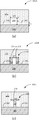
도 3(a)-3(c) 는 일부 실시예들에 따라 슬롯형 Y-커플링 도파관을 포함하는 변조기 장치의 횡단면도를 개략적으로 도시한다.
도 4 는 일부 실시예들에 따라 슬롯형 Y-커플링 도파관을 포함하는 변조기 장치 조립 방법에 대한 흐름도이다.
도 5 는 일부 실시예들에 따라 본원에 기술된 광학 상호접속 시스템의 일부가 될 수 있는 예시된 프로세서-기반 시스템을 개략적으로 도시한다.
Claims (20)
- 기판과,
상기 기판 상에 형성된 변조기 장치의 도파관을 포함하는 장치로서,
상기 도파관은,
상기 도파관을 따라서 전파되는 광을 수신하도록 구성되는 제 1 부분과,
상기 도파관에 형성되어 단일 슬롯으로 합쳐지는 제 1 의 두개의 슬롯을 포함하는 제 2 부분 - 상기 제 2 부분은 상기 제 1 부분과 결합됨 - 과,
상기 도파관에 형성되는 단일 슬롯을 포함하며, 상기 제 2 부분과 결합되는 제 3 부분과,
상기 도파관에 형성되며 상기 단일 슬롯으로부터 분기되는 제 2 의 두개의 슬롯을 포함하는 제 4 부분 - 상기 제 4 부분은 상기 제 3 부분과 결합됨 - 과,
상기 전파된 광을 출력하도록 구성되며, 상기 제 4 부분과 결합되는 제 5 부분을 포함하는
장치.
- 제 1 항에 있어서,
상기 기판은 유전체 물질을 포함하는
장치.
- 제 2 항에 있어서,
상기 기판은 실리콘 산화물(SiO2)을 포함하는
장치.
- 제 1 항에 있어서,
상기 도파관은 반도체 물질을 포함하는
장치.
- 제 4 항에 있어서,
상기 도파관은 실리콘을 포함하는
장치.
- 제 1 항에 있어서,
상기 제 2 부분의 상기 제 1 의 두개의 슬롯은 상기 도파관의 대향하는 에지들로부터 연장되고 상기 단일 슬롯으로 합쳐지며,
상기 제 4 부분의 상기 제 2 의 두개의 슬롯은 상기 단일 슬롯으로부터 분기되고 상기 도파관의 대향하는 에지들로 연장되는
장치.
- 제 6 항에 있어서,
상기 제 1 의 두개의 슬롯은 상기 도파관에서 광의 전파 방향으로 연장되는 제 1 가상선에 대해(across) 서로 대칭이며,
상기 제 2 의 두개의 슬롯은 상기 제 1 가상선에 대해 서로 대칭이며,
상기 제 1 의 두개의 슬롯 및 상기 제 2 의 두개의 슬롯은 상기 제 1 가상선에 수직인 제 2 가상선에 대해 서로 대칭인
장치.
- 제 1 항에 있어서,
상기 도파관의 제 1 부분 및 제 5 부분은 각각 상기 도파관을 통한 광 전파 방향으로 10 미크론 이상의 길이를 갖으며;
상기 도파관의 제 2 부분 및 제 4 부분은 각각 상기 도파관을 통한 광 전파 방향으로 50 미크론 이상의 길이를 갖으며;
상기 도파관의 제 3 부분은 상기 도파관을 통한 광 전파 방향으로 200 미크론 이상의 길이를 갖는
장치.
- 제 1 항에 있어서,
상기 제 2 부분의 상기 제 1 의 두개의 슬롯과, 상기 제 3 부분의 단일 슬롯과, 상기 제 4 부분의 상기 제 2 의 두개의 슬롯은 각각, 50 나노미터 내지 150 나노미터의 폭과 100 나노미터 내지 300 나노미터의 높이를 갖는
장치.
- 제 1 항에 있어서,
상기 제 2 부분의 상기 제 1 의 두개의 슬롯과, 상기 제 3 부분의 상기 단일 슬롯과, 상기 제 4 부분의 상기 제 2 의 두개의 슬롯은, 상기 도파관을 실질적으로 캡슐화하는 전기-광학(EO) 폴리머로 채워지는
장치. - 유전체 물질을 포함하는 기판을 제공하는 단계와,
상기 기판 상에 변조기 장치의 도파관 - 상기 도파관은 반도체 물질을 포함함 - 을 형성하는 단계를 포함하되,
상기 도파관은,
상기 도파관을 따라서 전파되는 광을 수신하도록 구성되는 제 1 부분과,
상기 도파관에 형성되어 단일 슬롯으로 합쳐지는 제 1 의 두개의 슬롯을 포함하는 제 2 부분 - 상기 제 2 부분은 상기 제 1 부분과 결합됨 - 과,
상기 도파관에 형성되는 단일 슬롯을 포함하며 상기 제 2 부분과 결합되는 제 3 부분과,
상기 도파관에 형성되며 상기 단일 슬롯으로부터 분기되는 제 2 의 두개의 슬롯을 포함하는 제 4 부분 - 상기 제 4 부분은 상기 제 3 부분과 결합됨 - 과,
상기 전파된 광을 출력하도록 구성되며 상기 제 4 부분과 결합되는 제 5 부분을 갖는
방법.
- 제 11 항에 있어서,
상기 도파관을 형성하는 단계는,
상기 기판 상에 상기 도파관의 상기 반도체 물질을 증착하는 단계와,
상기 제 2 부분의 상기 제 1 의 두개의 슬롯과, 상기 제 3 부분의 상기 단일 슬롯과, 상기 제 4 부분의 상기 제 2 의 두개의 슬롯을 형성하도록 상기 반도체 물질의 일부분을 제거하는 단계를 포함하는
방법.
- 제 12 항에 있어서,
상기 반도체 물질의 일부분을 제거하는 단계는,
증착된 상기 반도체 물질을 식각하는 이방성 식각 공정을 이용하는 단계를 포함하는
방법.
- 제 11 항에 있어서,
상기 제 2 부분의 상기 제 1 의 두개의 슬롯은 상기 도파관의 대향하는 에지들로부터 연장되고 상기 단일 슬롯으로 합쳐지며,
상기 제 4 부분의 상기 제 2 의 두개의 슬롯은 상기 단일 슬롯으로부터 분기되고 상기 도파관의 대향하는 에지들로 연장되는
방법.
- 제 11 항에 있어서,
상기 제 2 부분의 상기 제 1 의 두개의 슬롯과, 상기 제 3 부분의 상기 단일 슬롯과, 상기 제 4 부분의 상기 제 2 의 두개의 슬롯을 실질적으로 채우도록 전기-광학(EO) 폴리머를 증착시키는 단계를 더 포함하는
방법.
- 변조기 장치를 구동하도록 구성되는 프로세서와,
상기 프로세서와 결합되며 도파관을 포함하는 상기 변조기 장치를 포함하는 시스템으로서,
상기 도파관은,
상기 도파관을 따라서 전파되는 광을 수신하도록 구성되는 제 1 부분과,
상기 도파관에 형성되어 단일 슬롯으로 합쳐지는 제 1 의 두개의 슬롯을 포함하는 제 2 부분 - 상기 제 2 부분은 상기 제 1 부분과 결합됨 - 과,
상기 도파관에 형성되는 단일 슬롯을 포함하며, 상기 제 2 부분과 결합되는 제 3 부분과,
상기 도파관에 형성되며 상기 단일 슬롯으로부터 분기되는 제 2 의 두개의 슬롯을 포함하는 제 4 부분 - 상기 제 4 부분은 상기 제 3 부분과 결합됨 - 과,
상기 전파된 광을 출력하도록 구성되며 상기 제 4 부분과 결합되는 제 5 부분을 갖는
시스템.
- 제 16 항에 있어서,
상기 도파관을 따라서 전파되는 광을 제공하도록 상기 변조기와 결합된 레이저 광원과,
상기 도파관으로부터 다른 프로세서-기반 시스템으로 출력되는 광을 전달하며 상기 다른 프로세서-기반 시스템으로부터 수신되는 광을 전달하기 위한 접속기와,
상기 다른 프로세서-기반 시스템으로부터 수신되는 상기 접속기로부터의 광을 수신하기 위한 검출기 - 상기 프로세서는 상기 검출기로부터 수신된 신호를 처리하도록 구성됨 - 를 더 포함하는
시스템.
- 제 17 항에 있어서,
상기 다른 프로세서-기반 시스템과,
상기 접속기와 결합되며, 상기 변조기 장치로부터 상기 다른 프로세서-기반 시스템으로 광을 전달하며 상기 다른 프로세서-기반 시스템으로부터 상기 검출기로 광을 전달하도록 구성되는 섬유(fiber)를 더 포함하는
시스템.
- 제 16 항에 있어서,
상기 제 2 부분의 상기 제 1 의 두개의 슬롯은 상기 도파관의 대향하는 에지들로부터 연장되고 상기 단일 슬롯으로 합쳐지며,
상기 제 4 부분의 상기 제 2 의 두개의 슬롯들은 상기 단일 슬롯으로부터 분기되고 상기 도파관의 대향하는 에지들로 연장되는
시스템.
- 제 16 항에 있어서,
상기 시스템은 휴대용 컴퓨팅 장치, 태블릿, 또는 스마트폰인
시스템.
Applications Claiming Priority (1)
| Application Number | Priority Date | Filing Date | Title |
|---|---|---|---|
| PCT/US2011/052849 WO2013043183A1 (en) | 2011-09-22 | 2011-09-22 | Slotted y-coupling waveguide for slotted waveguide modulator device |
Publications (2)
| Publication Number | Publication Date |
|---|---|
| KR20140051443A true KR20140051443A (ko) | 2014-04-30 |
| KR101618189B1 KR101618189B1 (ko) | 2016-05-04 |
Family
ID=47914715
Family Applications (1)
| Application Number | Title | Priority Date | Filing Date |
|---|---|---|---|
| KR1020147007445A Active KR101618189B1 (ko) | 2011-09-22 | 2011-09-22 | 슬롯형 도파관 변조기 디바이스를 위한 슬롯형 y-커플링 도파관 |
Country Status (4)
| Country | Link |
|---|---|
| US (1) | US9025926B2 (ko) |
| KR (1) | KR101618189B1 (ko) |
| TW (1) | TWI483012B (ko) |
| WO (1) | WO2013043183A1 (ko) |
Families Citing this family (9)
| Publication number | Priority date | Publication date | Assignee | Title |
|---|---|---|---|---|
| US9939578B2 (en) | 2013-05-10 | 2018-04-10 | Intel Corporation | Low cost integration of optical components in planar lightwave circuits |
| CN103869414A (zh) * | 2014-04-08 | 2014-06-18 | 中国电子科技集团公司第四十四研究所 | 新型双y波导集成光学器件及其制作方法 |
| US11644618B2 (en) | 2018-06-22 | 2023-05-09 | Apple Inc. | Discrete optical unit on a substrate of an integrated photonics chip |
| US10823912B1 (en) * | 2018-09-27 | 2020-11-03 | Apple Inc. | Silicon photonics using off-cut wafer having top-side vertical outcoupler from etched cavity |
| US11525958B1 (en) | 2019-09-09 | 2022-12-13 | Apple Inc. | Off-cut wafer with a supported outcoupler |
| WO2022087479A1 (en) | 2020-10-23 | 2022-04-28 | Alexander Goldis | Fast-axis collimator with hanging connector |
| US12405420B2 (en) | 2021-09-23 | 2025-09-02 | Apple Inc. | Light output devices and light outputting methods for optical systems |
| US12292597B2 (en) | 2021-09-23 | 2025-05-06 | Apple Inc. | Light output devices and light outputting methods for optical systems |
| US20230280605A1 (en) * | 2022-03-07 | 2023-09-07 | Lightwave Logic Inc | Slot modulators with improved rf and bandwidth performance |
Family Cites Families (16)
| Publication number | Priority date | Publication date | Assignee | Title |
|---|---|---|---|---|
| US5138687A (en) * | 1989-09-26 | 1992-08-11 | Omron Corporation | Rib optical waveguide and method of manufacturing the same |
| JP3738469B2 (ja) * | 1995-07-27 | 2006-01-25 | 日立化成工業株式会社 | ポリイミド及びこれを用いた光部品 |
| GB2373343A (en) * | 2001-03-16 | 2002-09-18 | Bookham Technology Plc | Rib waveguide for connection to an optical component |
| US6633692B2 (en) * | 2001-07-31 | 2003-10-14 | The National University Of Singapore | High carrier injection optical waveguide switch |
| US7113676B2 (en) * | 2003-12-04 | 2006-09-26 | David Piede | Planar waveguide optical isolator in thin silicon-on-isolator (SOI) structure |
| JP4482486B2 (ja) | 2005-05-19 | 2010-06-16 | 日本電信電話株式会社 | 半導体スターカプラ型光合流分岐回路及び半導体アレイ回折格子 |
| CN101356655B (zh) * | 2005-11-10 | 2010-09-15 | 康乃尔研究基金会有限公司 | 发光缝隙波导器件 |
| JP4847176B2 (ja) * | 2006-03-29 | 2011-12-28 | 住友大阪セメント株式会社 | 光制御素子及びその製造方法 |
| FR2907916B1 (fr) * | 2006-10-31 | 2009-01-23 | Commissariat Energie Atomique | Nouvelle structure de guide a fente |
| KR100907250B1 (ko) * | 2007-12-10 | 2009-07-10 | 한국전자통신연구원 | 도파로 구조체 |
| US20090231686A1 (en) | 2008-01-12 | 2009-09-17 | Robert Atkins | Multi-functional integrated optical waveguides |
| US8768124B2 (en) * | 2009-01-05 | 2014-07-01 | Georgetown University | Direct coupling of optical slot waveguide to another optical waveguide |
| JP2012523580A (ja) * | 2009-04-10 | 2012-10-04 | コーニンクレッカ フィリップス エレクトロニクス エヌ ヴィ | 曲面スリット付き光ガイド曲がり |
| WO2010126525A1 (en) * | 2009-04-30 | 2010-11-04 | Hewlett-Packard Development Company, L.P. | Optical apparatus, system and method employing an endohedral metallofullerene |
| US8340486B1 (en) * | 2009-06-09 | 2012-12-25 | University Of Washington | Effective χ2 on the basis of electric biasing of χ3 materials |
| US8300990B2 (en) * | 2010-04-14 | 2012-10-30 | Oracle America, Inc. | Slotted optical waveguide with electro-optic material |
-
2011
- 2011-09-22 WO PCT/US2011/052849 patent/WO2013043183A1/en not_active Ceased
- 2011-09-22 KR KR1020147007445A patent/KR101618189B1/ko active Active
- 2011-09-22 US US13/581,720 patent/US9025926B2/en not_active Expired - Fee Related
-
2012
- 2012-08-31 TW TW101131832A patent/TWI483012B/zh not_active IP Right Cessation
Also Published As
| Publication number | Publication date |
|---|---|
| TWI483012B (zh) | 2015-05-01 |
| WO2013043183A1 (en) | 2013-03-28 |
| US20140199015A1 (en) | 2014-07-17 |
| TW201323951A (zh) | 2013-06-16 |
| KR101618189B1 (ko) | 2016-05-04 |
| US9025926B2 (en) | 2015-05-05 |
Similar Documents
| Publication | Publication Date | Title |
|---|---|---|
| KR101618189B1 (ko) | 슬롯형 도파관 변조기 디바이스를 위한 슬롯형 y-커플링 도파관 | |
| EP3807935B1 (en) | Vertical silicon-on-metal superconducting quantum interference device and method of production | |
| TWI582478B (zh) | 光學耦合器及形成光學裝置之光波導的方法 | |
| KR101591847B1 (ko) | 효율적인 실리콘-온-인슐레이터 격자 결합기 | |
| US8923665B2 (en) | Material structures for front-end of the line integration of optical polarization splitters and rotators | |
| US9696486B2 (en) | Surface-normal coupler for silicon-on-insulator platforms | |
| US20170168235A1 (en) | Chip-to-chip interconnect with embedded electro-optical bridge structures | |
| US11088311B2 (en) | Three-dimensional integration for qubits on multiple height crystalline dielectric | |
| US10937671B2 (en) | Conductive heat spreader and heat sink assembly for optical devices | |
| O'Connor et al. | Integrated optical interconnect architectures for embedded systems | |
| CN105637396A (zh) | 具有用于监控2×1光开关断开状态的集成光电二极管的2×1mmi的设备及方法 | |
| US12158625B2 (en) | Bidirectional optical grating coupler with multiple light paths for testing photonics devices | |
| US11550200B2 (en) | Reconfigurable optical grating/coupler | |
| US12429401B2 (en) | Tunable in-pool waveguide and method | |
| US20240111093A1 (en) | Glass recirculator for optical signal rerouting across photonic integrated circuits | |
| US20260118612A1 (en) | Diagonal directional coupler elevator | |
| WO2025264282A9 (en) | Waveguide located over deep oxide filled trench and method of making thereof | |
| CN116819678A (zh) | 包括超材料结构的槽形波导 |
Legal Events
| Date | Code | Title | Description |
|---|---|---|---|
| A201 | Request for examination | ||
| PA0105 | International application |
Patent event date: 20140320 Patent event code: PA01051R01D Comment text: International Patent Application |
|
| PA0201 | Request for examination | ||
| PG1501 | Laying open of application | ||
| E902 | Notification of reason for refusal | ||
| PE0902 | Notice of grounds for rejection |
Comment text: Notification of reason for refusal Patent event date: 20150703 Patent event code: PE09021S01D |
|
| E701 | Decision to grant or registration of patent right | ||
| PE0701 | Decision of registration |
Patent event code: PE07011S01D Comment text: Decision to Grant Registration Patent event date: 20160128 |
|
| GRNT | Written decision to grant | ||
| PR0701 | Registration of establishment |
Comment text: Registration of Establishment Patent event date: 20160428 Patent event code: PR07011E01D |
|
| PR1002 | Payment of registration fee |
Payment date: 20160429 End annual number: 3 Start annual number: 1 |
|
| PG1601 | Publication of registration | ||
| FPAY | Annual fee payment |
Payment date: 20190328 Year of fee payment: 4 |
|
| PR1001 | Payment of annual fee |
Payment date: 20190328 Start annual number: 4 End annual number: 4 |
|
| PR1001 | Payment of annual fee |
Payment date: 20210329 Start annual number: 6 End annual number: 6 |
|
| PR1001 | Payment of annual fee |
Payment date: 20220329 Start annual number: 7 End annual number: 7 |
|
| PR1001 | Payment of annual fee |
Payment date: 20230329 Start annual number: 8 End annual number: 8 |
|
| PR1001 | Payment of annual fee |
Payment date: 20231205 Start annual number: 9 End annual number: 9 |
|
| PR1001 | Payment of annual fee |
Payment date: 20241128 Start annual number: 10 End annual number: 10 |