KR20140055029A - 크로스토크를 감소시키는 실리콘 광증배관 소자 - Google Patents
크로스토크를 감소시키는 실리콘 광증배관 소자 Download PDFInfo
- Publication number
- KR20140055029A KR20140055029A KR1020120121269A KR20120121269A KR20140055029A KR 20140055029 A KR20140055029 A KR 20140055029A KR 1020120121269 A KR1020120121269 A KR 1020120121269A KR 20120121269 A KR20120121269 A KR 20120121269A KR 20140055029 A KR20140055029 A KR 20140055029A
- Authority
- KR
- South Korea
- Prior art keywords
- micro
- silicon
- pixels
- present
- trench
- Prior art date
- Legal status (The legal status is an assumption and is not a legal conclusion. Google has not performed a legal analysis and makes no representation as to the accuracy of the status listed.)
- Ceased
Links
- XUIMIQQOPSSXEZ-UHFFFAOYSA-N Silicon Chemical compound [Si] XUIMIQQOPSSXEZ-UHFFFAOYSA-N 0.000 title claims abstract description 43
- 229910052710 silicon Inorganic materials 0.000 title claims abstract description 43
- 239000010703 silicon Substances 0.000 title claims abstract description 43
- 230000003287 optical effect Effects 0.000 title description 5
- 239000000463 material Substances 0.000 claims abstract description 13
- 238000000034 method Methods 0.000 claims description 10
- XAGFODPZIPBFFR-UHFFFAOYSA-N aluminium Chemical compound [Al] XAGFODPZIPBFFR-UHFFFAOYSA-N 0.000 claims description 7
- 229910052782 aluminium Inorganic materials 0.000 claims description 7
- 239000004642 Polyimide Substances 0.000 claims description 4
- 229920001721 polyimide Polymers 0.000 claims description 4
- 238000005530 etching Methods 0.000 claims description 3
- 238000002955 isolation Methods 0.000 claims description 3
- 239000000758 substrate Substances 0.000 description 18
- 230000005684 electric field Effects 0.000 description 8
- 238000010586 diagram Methods 0.000 description 4
- 238000001514 detection method Methods 0.000 description 3
- 238000005259 measurement Methods 0.000 description 3
- 229920002120 photoresistant polymer Polymers 0.000 description 3
- 230000002411 adverse Effects 0.000 description 2
- 150000002500 ions Chemical class 0.000 description 2
- 238000012986 modification Methods 0.000 description 2
- 230000004048 modification Effects 0.000 description 2
- 230000001699 photocatalysis Effects 0.000 description 2
- VYPSYNLAJGMNEJ-UHFFFAOYSA-N Silicium dioxide Chemical compound O=[Si]=O VYPSYNLAJGMNEJ-UHFFFAOYSA-N 0.000 description 1
- 230000015556 catabolic process Effects 0.000 description 1
- 238000010276 construction Methods 0.000 description 1
- 238000001803 electron scattering Methods 0.000 description 1
- 239000000945 filler Substances 0.000 description 1
- 239000007943 implant Substances 0.000 description 1
- 238000006303 photolysis reaction Methods 0.000 description 1
- 229910021420 polycrystalline silicon Inorganic materials 0.000 description 1
- 229920005591 polysilicon Polymers 0.000 description 1
- 230000035945 sensitivity Effects 0.000 description 1
- 229910052814 silicon oxide Inorganic materials 0.000 description 1
Images

Classifications
-
- H—ELECTRICITY
- H10—SEMICONDUCTOR DEVICES; ELECTRIC SOLID-STATE DEVICES NOT OTHERWISE PROVIDED FOR
- H10F—INORGANIC SEMICONDUCTOR DEVICES SENSITIVE TO INFRARED RADIATION, LIGHT, ELECTROMAGNETIC RADIATION OF SHORTER WAVELENGTH OR CORPUSCULAR RADIATION
- H10F30/00—Individual radiation-sensitive semiconductor devices in which radiation controls the flow of current through the devices, e.g. photodetectors
- H10F30/20—Individual radiation-sensitive semiconductor devices in which radiation controls the flow of current through the devices, e.g. photodetectors the devices having potential barriers, e.g. phototransistors
-
- H—ELECTRICITY
- H10—SEMICONDUCTOR DEVICES; ELECTRIC SOLID-STATE DEVICES NOT OTHERWISE PROVIDED FOR
- H10F—INORGANIC SEMICONDUCTOR DEVICES SENSITIVE TO INFRARED RADIATION, LIGHT, ELECTROMAGNETIC RADIATION OF SHORTER WAVELENGTH OR CORPUSCULAR RADIATION
- H10F19/00—Integrated devices, or assemblies of multiple devices, comprising at least one photovoltaic cell covered by group H10F10/00, e.g. photovoltaic modules
- H10F19/10—Integrated devices, or assemblies of multiple devices, comprising at least one photovoltaic cell covered by group H10F10/00, e.g. photovoltaic modules comprising photovoltaic cells in arrays in a single semiconductor substrate, the photovoltaic cells having vertical junctions or V-groove junctions
-
- H—ELECTRICITY
- H10—SEMICONDUCTOR DEVICES; ELECTRIC SOLID-STATE DEVICES NOT OTHERWISE PROVIDED FOR
- H10F—INORGANIC SEMICONDUCTOR DEVICES SENSITIVE TO INFRARED RADIATION, LIGHT, ELECTROMAGNETIC RADIATION OF SHORTER WAVELENGTH OR CORPUSCULAR RADIATION
- H10F99/00—Subject matter not provided for in other groups of this subclass
-
- Y—GENERAL TAGGING OF NEW TECHNOLOGICAL DEVELOPMENTS; GENERAL TAGGING OF CROSS-SECTIONAL TECHNOLOGIES SPANNING OVER SEVERAL SECTIONS OF THE IPC; TECHNICAL SUBJECTS COVERED BY FORMER USPC CROSS-REFERENCE ART COLLECTIONS [XRACs] AND DIGESTS
- Y02—TECHNOLOGIES OR APPLICATIONS FOR MITIGATION OR ADAPTATION AGAINST CLIMATE CHANGE
- Y02E—REDUCTION OF GREENHOUSE GAS [GHG] EMISSIONS, RELATED TO ENERGY GENERATION, TRANSMISSION OR DISTRIBUTION
- Y02E10/00—Energy generation through renewable energy sources
- Y02E10/50—Photovoltaic [PV] energy
Landscapes
- Light Receiving Elements (AREA)
Abstract
Description
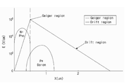
도 2는 일반적인 실리콘 광증배관 소자에서 에피택시층 내 전기장의 분포를 나타내는 도면이다.
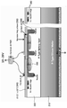
도 3은 본 발명의 일 실시예에 따른 크로스토크를 감소시키는 실리콘 광증배관 소자의 단면을 나타내는 도면이다.
도 4는 크로스토크 현상을 설명하기 위한 도면이다.
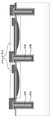
도 5는 도 3에 도시된 트랜치 구조를 구체적으로 도시한 도면이다.
230: PN 접합층 240: 절연층
250: 저항 260: 알루미늄 구성
270: 트랜치 구조 275: 충전 물질
280: 가드링
Claims (5)
- 다수의 마이크로 픽셀로 이루어진 실리콘 광증배관 소자(Silicon Photomultiplier)에 있어서,
상기 마이크로 픽셀들을 광학적으로 서로 분리시키는 다수의 트랜치 구조; 및
상기 트랜치 구조 내부에 채워져 상기 마이크로 픽셀 간의 크로스토크 현상을 감소시키는 충전 물질을 포함하는 실리콘 광증배관 소자.
- 제 1 항에 있어서,
상기 트랜치 구조는 STI(Shallow Trench Isolation) 공정에 따른 식각에 의해 형성되는 실리콘 광증배관 소자.
- 제 1 항에 있어서,
상기 트랜치 구조는 일자 구조, U자 구조, V자 구조 중 어느 하나의 형태로 형성되는 실리콘 광증배관 소자.
- 제 1 항에 있어서,
상기 충전 물질은 폴리이미드(Polyimide)인 실리콘 광증배관 소자.
- 제 1 항에 있어서,
상기 충전 물질은 알루미늄(Al)인 실리콘 광증배관 소자.
Priority Applications (1)
| Application Number | Priority Date | Filing Date | Title |
|---|---|---|---|
| KR1020120121269A KR20140055029A (ko) | 2012-10-30 | 2012-10-30 | 크로스토크를 감소시키는 실리콘 광증배관 소자 |
Applications Claiming Priority (1)
| Application Number | Priority Date | Filing Date | Title |
|---|---|---|---|
| KR1020120121269A KR20140055029A (ko) | 2012-10-30 | 2012-10-30 | 크로스토크를 감소시키는 실리콘 광증배관 소자 |
Publications (1)
| Publication Number | Publication Date |
|---|---|
| KR20140055029A true KR20140055029A (ko) | 2014-05-09 |
Family
ID=50886771
Family Applications (1)
| Application Number | Title | Priority Date | Filing Date |
|---|---|---|---|
| KR1020120121269A Ceased KR20140055029A (ko) | 2012-10-30 | 2012-10-30 | 크로스토크를 감소시키는 실리콘 광증배관 소자 |
Country Status (1)
| Country | Link |
|---|---|
| KR (1) | KR20140055029A (ko) |
Cited By (1)
| Publication number | Priority date | Publication date | Assignee | Title |
|---|---|---|---|---|
| KR20200085911A (ko) * | 2016-01-15 | 2020-07-15 | 소니 뎁쓰센싱 솔루션즈 에스에이/엔브이 | 다수 전류 및 분리 수단을 갖는 검출기 디바이스 |
-
2012
- 2012-10-30 KR KR1020120121269A patent/KR20140055029A/ko not_active Ceased
Cited By (1)
| Publication number | Priority date | Publication date | Assignee | Title |
|---|---|---|---|---|
| KR20200085911A (ko) * | 2016-01-15 | 2020-07-15 | 소니 뎁쓰센싱 솔루션즈 에스에이/엔브이 | 다수 전류 및 분리 수단을 갖는 검출기 디바이스 |
Similar Documents
| Publication | Publication Date | Title |
|---|---|---|
| US10347670B2 (en) | Photodetection element | |
| US9716121B1 (en) | Majority current assisted radiation detector device | |
| CN105448945B (zh) | 同面电极光电二极管阵列及其制作方法 | |
| CN108231947B (zh) | 一种单光子雪崩二极管探测器结构及其制造方法 | |
| KR100879013B1 (ko) | 매립형 컬렉터를 구비하는 포토트랜지스터 | |
| US9698196B2 (en) | Demodulation pixel incorporating majority carrier current, buried channel and high-low junction | |
| CN108231946B (zh) | 一种单光子雪崩二极管探测器结构及其制造方法 | |
| EP2816601A1 (en) | Improvements in or relating to pinned photodiodes for use in image sensors | |
| CN102024863B (zh) | 高速增强型紫外硅选择性雪崩光电二极管及其制作方法 | |
| CN103887362A (zh) | 一种带有深n阱的np型cmos雪崩光电二极管 | |
| CN103904152B (zh) | 光电探测器及其制造方法和辐射探测器 | |
| EP1864336B1 (en) | Minimizing the effect of directly converted x-rays in x-ray imagers | |
| US20220254818A1 (en) | Image sensing device | |
| CN107895743B (zh) | 单光子雪崩光电二极管探测器的装置和方法 | |
| US9768340B2 (en) | Photodiode with a dark current suppression junction | |
| JP5165588B2 (ja) | 可視光を検出するために最適化された半導体放射線検出器 | |
| US11316063B2 (en) | Diode devices and methods of forming a diode device | |
| KR101638545B1 (ko) | 누설전류를 방지하는 실리콘 광증배관 소자 | |
| KR20140055029A (ko) | 크로스토크를 감소시키는 실리콘 광증배관 소자 | |
| KR20180035334A (ko) | 크로스토크를 감소시키는 실리콘 광증배관 소자 | |
| KR101330270B1 (ko) | 소비전력 및 암전류가 감소된 실리콘 광전자 증배관 | |
| KR20180035327A (ko) | 광검출 효율이 향상된 실리콘 광증배관 소자 | |
| CN119545927A (zh) | 雪崩二极管和探测器 | |
| KR101707896B1 (ko) | 실리콘 광 증배 소자 | |
| RU2316848C1 (ru) | Микроканальный лавинный фотодиод |
Legal Events
| Date | Code | Title | Description |
|---|---|---|---|
| A201 | Request for examination | ||
| PA0109 | Patent application |
Patent event code: PA01091R01D Comment text: Patent Application Patent event date: 20121030 |
|
| PA0201 | Request for examination | ||
| E902 | Notification of reason for refusal | ||
| PE0902 | Notice of grounds for rejection |
Comment text: Notification of reason for refusal Patent event date: 20130926 Patent event code: PE09021S01D |
|
| N231 | Notification of change of applicant | ||
| PN2301 | Change of applicant |
Patent event date: 20131114 Comment text: Notification of Change of Applicant Patent event code: PN23011R01D |
|
| E902 | Notification of reason for refusal | ||
| PE0902 | Notice of grounds for rejection |
Comment text: Notification of reason for refusal Patent event date: 20140328 Patent event code: PE09021S01D |
|
| PG1501 | Laying open of application | ||
| E90F | Notification of reason for final refusal | ||
| PE0902 | Notice of grounds for rejection |
Comment text: Final Notice of Reason for Refusal Patent event date: 20140627 Patent event code: PE09021S02D |
|
| E601 | Decision to refuse application | ||
| PE0601 | Decision on rejection of patent |
Patent event date: 20140930 Comment text: Decision to Refuse Application Patent event code: PE06012S01D Patent event date: 20140627 Comment text: Final Notice of Reason for Refusal Patent event code: PE06011S02I Patent event date: 20140328 Comment text: Notification of reason for refusal Patent event code: PE06011S01I Patent event date: 20130926 Comment text: Notification of reason for refusal Patent event code: PE06011S01I |