KR20140074009A - Adaptive power converting device - Google Patents
Adaptive power converting device Download PDFInfo
- Publication number
- KR20140074009A KR20140074009A KR1020120142129A KR20120142129A KR20140074009A KR 20140074009 A KR20140074009 A KR 20140074009A KR 1020120142129 A KR1020120142129 A KR 1020120142129A KR 20120142129 A KR20120142129 A KR 20120142129A KR 20140074009 A KR20140074009 A KR 20140074009A
- Authority
- KR
- South Korea
- Prior art keywords
- voltage
- gate
- slew rate
- switching
- power
- Prior art date
- Legal status (The legal status is an assumption and is not a legal conclusion. Google has not performed a legal analysis and makes no representation as to the accuracy of the status listed.)
- Granted
Links
Images









Classifications
-
- H—ELECTRICITY
- H02—GENERATION; CONVERSION OR DISTRIBUTION OF ELECTRIC POWER
- H02M—APPARATUS FOR CONVERSION BETWEEN AC AND AC, BETWEEN AC AND DC, OR BETWEEN DC AND DC, AND FOR USE WITH MAINS OR SIMILAR POWER SUPPLY SYSTEMS; CONVERSION OF DC OR AC INPUT POWER INTO SURGE OUTPUT POWER; CONTROL OR REGULATION THEREOF
- H02M3/00—Conversion of DC power input into DC power output
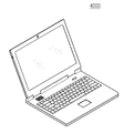
- H02M3/02—Conversion of DC power input into DC power output without intermediate conversion into AC
- H02M3/04—Conversion of DC power input into DC power output without intermediate conversion into AC by static converters
- H02M3/10—Conversion of DC power input into DC power output without intermediate conversion into AC by static converters using discharge tubes with control electrode or semiconductor devices with control electrode
- H02M3/145—Conversion of DC power input into DC power output without intermediate conversion into AC by static converters using discharge tubes with control electrode or semiconductor devices with control electrode using devices of a triode or transistor type requiring continuous application of a control signal
- H02M3/155—Conversion of DC power input into DC power output without intermediate conversion into AC by static converters using discharge tubes with control electrode or semiconductor devices with control electrode using devices of a triode or transistor type requiring continuous application of a control signal using semiconductor devices only
- H02M3/156—Conversion of DC power input into DC power output without intermediate conversion into AC by static converters using discharge tubes with control electrode or semiconductor devices with control electrode using devices of a triode or transistor type requiring continuous application of a control signal using semiconductor devices only with automatic control of output voltage or current, e.g. switching regulators
- H02M3/158—Conversion of DC power input into DC power output without intermediate conversion into AC by static converters using discharge tubes with control electrode or semiconductor devices with control electrode using devices of a triode or transistor type requiring continuous application of a control signal using semiconductor devices only with automatic control of output voltage or current, e.g. switching regulators including plural semiconductor devices as final control devices for a single load
- H02M3/1588—Conversion of DC power input into DC power output without intermediate conversion into AC by static converters using discharge tubes with control electrode or semiconductor devices with control electrode using devices of a triode or transistor type requiring continuous application of a control signal using semiconductor devices only with automatic control of output voltage or current, e.g. switching regulators including plural semiconductor devices as final control devices for a single load comprising at least one synchronous rectifier element
-
- H—ELECTRICITY
- H02—GENERATION; CONVERSION OR DISTRIBUTION OF ELECTRIC POWER
- H02M—APPARATUS FOR CONVERSION BETWEEN AC AND AC, BETWEEN AC AND DC, OR BETWEEN DC AND DC, AND FOR USE WITH MAINS OR SIMILAR POWER SUPPLY SYSTEMS; CONVERSION OF DC OR AC INPUT POWER INTO SURGE OUTPUT POWER; CONTROL OR REGULATION THEREOF
- H02M3/00—Conversion of DC power input into DC power output
- H02M3/02—Conversion of DC power input into DC power output without intermediate conversion into AC
- H02M3/04—Conversion of DC power input into DC power output without intermediate conversion into AC by static converters
- H02M3/10—Conversion of DC power input into DC power output without intermediate conversion into AC by static converters using discharge tubes with control electrode or semiconductor devices with control electrode
- H02M3/145—Conversion of DC power input into DC power output without intermediate conversion into AC by static converters using discharge tubes with control electrode or semiconductor devices with control electrode using devices of a triode or transistor type requiring continuous application of a control signal
- H02M3/155—Conversion of DC power input into DC power output without intermediate conversion into AC by static converters using discharge tubes with control electrode or semiconductor devices with control electrode using devices of a triode or transistor type requiring continuous application of a control signal using semiconductor devices only
-
- H—ELECTRICITY
- H03—ELECTRONIC CIRCUITRY
- H03K—PULSE TECHNIQUE
- H03K17/00—Electronic switching or gating, i.e. not by contact-making and –breaking
- H03K17/16—Modifications for eliminating interference voltages or currents
- H03K17/161—Modifications for eliminating interference voltages or currents in field-effect transistor switches
- H03K17/165—Modifications for eliminating interference voltages or currents in field-effect transistor switches by feedback from the output circuit to the control circuit
- H03K17/166—Soft switching
-
- H—ELECTRICITY
- H03—ELECTRONIC CIRCUITRY
- H03K—PULSE TECHNIQUE
- H03K17/00—Electronic switching or gating, i.e. not by contact-making and –breaking
- H03K17/16—Modifications for eliminating interference voltages or currents
- H03K17/161—Modifications for eliminating interference voltages or currents in field-effect transistor switches
- H03K17/165—Modifications for eliminating interference voltages or currents in field-effect transistor switches by feedback from the output circuit to the control circuit
- H03K17/166—Soft switching
- H03K17/167—Soft switching using parallel switching arrangements
-
- Y—GENERAL TAGGING OF NEW TECHNOLOGICAL DEVELOPMENTS; GENERAL TAGGING OF CROSS-SECTIONAL TECHNOLOGIES SPANNING OVER SEVERAL SECTIONS OF THE IPC; TECHNICAL SUBJECTS COVERED BY FORMER USPC CROSS-REFERENCE ART COLLECTIONS [XRACs] AND DIGESTS
- Y02—TECHNOLOGIES OR APPLICATIONS FOR MITIGATION OR ADAPTATION AGAINST CLIMATE CHANGE
- Y02B—CLIMATE CHANGE MITIGATION TECHNOLOGIES RELATED TO BUILDINGS, e.g. HOUSING, HOUSE APPLIANCES OR RELATED END-USER APPLICATIONS
- Y02B70/00—Technologies for an efficient end-user side electric power management and consumption
- Y02B70/10—Technologies improving the efficiency by using switched-mode power supplies [SMPS], i.e. efficient power electronics conversion e.g. power factor correction or reduction of losses in power supplies or efficient standby modes
Landscapes
- Engineering & Computer Science (AREA)
- Power Engineering (AREA)
- Dc-Dc Converters (AREA)
Abstract
스위칭 전압 스파이크를 적응적으로 제어하는 어댑티브 전원 컨버팅 장치가 개시된다. 본 발명에 따른 전원 컨버팅 장치는, 게이트로 인가되는 입력에 따라 전원전압을 구동하여 스위칭 출력노드로 인가하는 파워 스위치를 포함하는 컨버팅 회로와, 상기 파워 스위치의 상기 게이트와 그라운드 간에 연결되어 상기 스위칭 출력노드의 출력 전압에서 나타나는 전압 스파이크의 사이즈를 줄이면서도 파워 효율을 증가시키기 위해 상기 출력 전압의 슬루 레이트를 조절하는 슬루 리미터를 포함함에 의해, 스위칭 전압 스파이크가 적응적으로 제어된다. An adaptive power conversion device is disclosed that adaptively controls switching voltage spikes. A power conversion apparatus according to the present invention includes: a converting circuit including a power switch for driving a power supply voltage according to an input applied to a gate to apply to a switching output node; and a switching circuit connected between the gate and the ground of the power switch, By including a slew limiter that adjusts the slew rate of the output voltage to increase the power efficiency while reducing the size of the voltage spike that appears at the output voltage of the node, the switching voltage spike is adaptively controlled.
Description
본 발명은 전원 컨버팅 장치에 관한 것으로, 보다 구체적으로 DC-DC 컨버터 등과 같은 전원 컨버팅 장치에 관한 것이다.
BACKGROUND OF THE
전형적인 스위칭 벅 컨버터(Switching Buck Converter)는 설정된 DC 전압을 생성하기 위해 파워 스위치를 이용하여 파워 스위칭을 수행한다. A typical switching buck converter performs power switching using a power switch to generate a set DC voltage.
파워 스위칭의 온/오프(ON/OFF)동작에 의해 발생되는 급작스런 전류(current) 흐름의 변화는 스위칭 출력 노드에 전압 스파이크(voltage spikes)를 유발한다. 전압 스파이크는 내부 와이어본드 인덕턴스(wirebond inductance) 및 PCB 디자인(design)의 기생 인덕턴스(parasitic inductance)에 기인하여 발생된다. A sudden change in current flow caused by on / off operation of the power switching causes voltage spikes at the switching output node. Voltage spikes are caused by internal wire bond inductance and parasitic inductance of the PCB design.
전압 스파이크를 없애거나 줄이는 일반적인 테크닉은 파워 스위치의 스위칭 온/오프 속도 즉, 스위칭 슬루 레이트(switching slew rate)을 느리게 제어하는 것이다. 그러나 슬루 레이트를 고정된 슬루 레이트에 맞춰 느리게 하는 것은 스위치 컨덕션 파워 로스(switch conduction power loss)를 더 크게 하는 현상을 유발할 수 있다. 결국, 슬루 레이트를 마냥 느리게만 할 경우에 파워 효율(power efficiency)이 그에 따라 저하된다. 이와 같이 슬루 레이트를 느리게 하여 전압 스파이크를 줄이는 것과 파워 효율의 유지는 트레이드 오프(trade off)의 관계를 가진다.
A common technique for eliminating or reducing voltage spikes is to slowly control the switching on / off speed of the power switch, i.e., the switching slew rate. However, slowing the slew rate to a fixed slew rate can cause the switch conduction power loss to become larger. As a result, when the slew rate is slow, the power efficiency is lowered accordingly. Thus, there is a trade-off relationship between slowing the slew rate and reducing voltage spikes and maintaining power efficiency.
본 발명이 해결하고자 하는 기술적 과제는, 파워 효율의 저하를 최소화하면서도 전압 스파이크를 최소화 또는 줄일 수 있는 전원 컨버팅 장치를 제공함에 있다. SUMMARY OF THE INVENTION It is an object of the present invention to provide a power conversion device capable of minimizing or reducing voltage spikes while minimizing degradation of power efficiency.
본 발명이 해결하고자 하는 기술적 과제는, 부하 전류(load current)의 변동이나 외부 어플리케이션 보드(application boards)의 환경에 따라 스위칭 슬루 레이트를 적응적(adaptive)으로 조절함에 의해 전압 스파이크(voltage spikes)를 줄이는 동시에 파워 로스(power loss)를 최소화 또는 줄일 수 있는 전원 컨버팅 장치를 제공함에 있다.
SUMMARY OF THE INVENTION The present invention is directed to adaptively adjusting a switching slew rate according to variations in a load current or an application board environment of an external application board so that voltage spikes And at the same time minimizing or reducing power loss.
상기 기술적 과제를 달성하기 위한 본 발명의 개념의 일 양상(an aspect)에 따른 전원 컨버팅 장치는, According to an aspect of the present invention, there is provided a power conversion apparatus comprising:
게이트로 인가되는 입력에 따라 구동 전원전압을 구동하여 스위칭 출력노드로 인가하는 파워 스위치를 포함하는 컨버팅 회로; 및A converting circuit including a power switch for driving a driving power supply voltage according to an input applied to a gate and applying the driving power supply voltage to a switching output node; And
상기 파워 스위치의 상기 게이트와 그라운드 간에 연결되어 상기 스위칭 출력노드의 출력 전압에서 나타나는 전압 스파이크의 사이즈를 줄이면서도 파워 효율을 증가시키기 위해 상기 출력 전압의 슬루 레이트를 조절하는 슬루 리미터를 포함한다. And a slew limiter connected between the gate of the power switch and the ground to adjust the slew rate of the output voltage to increase the power efficiency while reducing the size of the voltage spike appearing at the output voltage of the switching output node.
본 발명의 개념적 실시 예에 있어서, 상기 슬루 리미터는 상기 파워 스위치의 게이트-소스 커패시턴스에 비해 작은 커패시턴스를 갖는 커패시터일 수 있다. In a conceptual embodiment of the present invention, the slew limiter may be a capacitor having a capacitance that is less than the gate-source capacitance of the power switch.
본 발명의 개념적 실시 예에 있어서, 상기 파워 스위치의 상기 게이트와 상기 슬루 리미터 간에 연결되어 상기 슬루 리미터를 통해 흐르는 전류를 부하 변동에 따라 적응적으로 조절하는 슬루 레이트 콘트롤러를 더 포함할 수 있다. In the conceptual embodiment of the present invention, the controller may further include a slew rate controller connected between the gate of the power switch and the slew limiter, and adapted to adaptively adjust a current flowing through the slew limiter according to a load variation.
본 발명의 개념적 실시 예에 있어서, 상기 슬루 레이트 콘트롤러는 제어전압 신호에 따라 저항값이 가변되는 가변저항으로서 기능하는 모스 트랜지스터일 수 있다. In the conceptual embodiment of the present invention, the slew rate controller may be a MOS transistor functioning as a variable resistor whose resistance value varies according to a control voltage signal.
본 발명의 개념적 실시 예에 있어서, 상기 스위칭 출력노드의 출력 전압을 모니터링하여 상기 제어전압 신호를 생성하는 어댑티브 스위칭 콘트롤러를 더 포함할 수 있다. In a conceptual embodiment of the present invention, the adaptive switching controller may further comprise an adaptive switching controller for monitoring the output voltage of the switching output node to generate the control voltage signal.
본 발명의 개념적 실시 예에 있어서, 상기 어댑티브 스위칭 콘트롤러는,In a conceptual embodiment of the present invention, the adaptive switching controller comprises:
제1 동작구간에서 인가되는 상기 스위칭 출력노드의 출력 전압을 샘플링 및 홀드하는 샘플 앤드 홀드 회로;A sample and hold circuit for sampling and holding the output voltage of the switching output node applied in the first operation period;
상기 제1 동작구간의 다음 구간인 제2 동작구간에서 인가되는 상기 스위칭 출력노드의 출력 전압을 상기 샘플 앤드 홀드 회로의 출력과 비교하여 전압 스파이크 검출의 유무를 가리키는 비교 신호를 출력하는 비교기; 및A comparator for comparing the output voltage of the switching output node applied in a second operation period, which is a next section between the first operation ports, with an output of the sample and hold circuit to output a comparison signal indicating whether or not voltage spike detection is performed; And
상기 비교 신호의 레벨에 따라 슬루 레이트 조절을 위해 차징 업 또는 디스차아징되는 전압을 생성하여 상기 제어전압 신호로서 출력하는 인터그레이터를 포함할 수 있다. And an integrator for generating a charged up or dischaged voltage for the slew rate control according to the level of the comparison signal and outputting the generated voltage as the control voltage signal.
본 발명의 개념적 실시 예에 있어서, 상기 인터그레이터의 디스차아징 경로에는 역류 방지 기능을 위한 다이오드가 추가적으로 설치될 수 있다. In the conceptual embodiment of the present invention, a diode for preventing the backflow may be additionally installed in the discharging path of the integrator.
본 발명의 개념적 실시 예에 있어서, 상기 샘플 앤드 홀드 회로는 샘플링된 상기 스위칭 출력노드의 출력 전압을 홀드 시에 전압 스파이크의 허용 설계 값인 문턱전압 값을 상기 샘플링된 출력 전압에 더하여 홀드할 수 있다. In a conceptual embodiment of the invention, the sample and hold circuit may hold the sampled output voltage of the switching output node by adding to the sampled output voltage a threshold voltage value that is the allowable design value of the voltage spike at the time of hold.
본 발명의 개념적 실시 예에 있어서, 상기 제1,2 동작 구간들의 주기는 상기 파워 스위치의 상기 게이트에 인가되는 입력의 주기에 대응될 수 있다. In a conceptual embodiment of the present invention, the period of the first and second operating intervals may correspond to the period of the input applied to the gate of the power switch.
본 발명의 개념적 실시 예에 있어서, 상기 입력은 펄스 폭 변조 신호일 수 있다. In a conceptual embodiment of the present invention, the input may be a pulse width modulated signal.
본 발명의 개념적 실시 예에 있어서, 상기 컨버팅 회로는 DC-DC 벅 컨버터일 수 있다. In a conceptual embodiment of the present invention, the converting circuit may be a DC-DC buck converter.
상기 기술적 과제를 달성하기 위한 본 발명의 개념의 다른 양상(another aspect)에 따라, According to another aspect of the inventive concept to accomplish the above object,
게이트로 인가되는 입력에 따라 구동 전원전압을 구동하여 스위칭 출력노드로 인가하는 파워 스위치를 포함하는 컨버팅 회로에서의 슬루 레이트 제어방법은:A method for controlling slew rate in a converting circuit comprising a power switch for driving a driving power supply voltage according to an input applied to a gate to apply to a switching output node, comprising:
상기 파워 스위치의 상기 게이트와 그라운드 간에 슬루 레이트 콘트롤러와 슬루 리미터를 설치하고,A slew rate controller and a slew limiter are provided between the gate and the ground of the power switch,
상기 스위칭 출력노드의 출력 전압에서 나타나는 전압 스파이크의 사이즈가 허용치를 초과하였는 지를 모니터링하고,Monitoring whether the size of the voltage spike at the output voltage of the switching output node exceeds a tolerance,
상기 모니터링 결과에 의존하여 상기 슬루 레이트 콘트롤러를 구동함에 의해 상기 출력 전압의 슬루 레이트가 조절되도록 한다. And the slew rate of the output voltage is adjusted by driving the slew rate controller depending on the monitoring result.
본 발명의 개념적 실시 예에 있어서, 상기 슬루 리미터는 상기 파워 스위치의 게이트-소스 커패시턴스에 비해 작은 커패시턴스를 갖는 커패시터이고, 상기 슬루 레이트 콘트롤러는 게이트 전압에 따라 저항값이 가변되는 트랜지스터일 수 있다. In the conceptual embodiment of the present invention, the slew limiter is a capacitor having a capacitance smaller than the gate-source capacitance of the power switch, and the slew rate controller may be a transistor whose resistance value varies according to the gate voltage.
본 발명의 개념적 실시 예에 있어서, 상기 전압 스파이크의 사이즈가 허용치를 초과한 경우에 상기 게이트 전압은 상승되어 상기 출력 전압의 슬루 레이트는 낮아지고, 상기 전압 스파이크의 사이즈가 허용치 이하인 경우에 상기 게이트 전압은 하강되어 상기 출력 전압의 슬루 레이트는 높아질 수 있다. In a conceptual embodiment of the present invention, when the size of the voltage spike exceeds a tolerance, the gate voltage is raised to lower the slew rate of the output voltage, and when the size of the voltage spike is less than the allowable value, The slew rate of the output voltage can be increased.
본 발명의 개념적 실시 예에 있어서, 상기 슬루 레이트의 조절은, 상기 전압 스파이크의 사이즈를 줄이면서도 파워 효율을 증가시키기 위해 상기 파워 스위치의 게이트로 인가되는 입력의 주기마다 적응적으로 실행될 수 있다.
In a conceptual embodiment of the invention, the adjustment of the slew rate may be adaptively performed every period of the input applied to the gate of the power switch to increase the power efficiency while reducing the size of the voltage spike.
본 발명의 실시 예적인 구성에 따르면, 스위칭 슬루 레이트가 적응적(adaptively)으로 조절되는 것에 의해 전압 스파이크가 줄어드는 동시에 파워 로스도 최소화 또는 줄어든다. According to an exemplary configuration of the present invention, the switching slew rate is adaptively adjusted so that voltage spikes are reduced while power loss is minimized or reduced.
또한, 다양한 어플리케이션 보드(application boards)의 환경 하에서도 전압 스파이크 수준이 동일한 레벨로서 유지된다.
Also, the voltage spike levels are maintained at the same level under the environment of various application boards.
도 1은 일반적인 벅 컨버터를 보여주는 컨버팅 회로 블록도,
도 2는 도 1의 컨버팅 회로 노드들에 나타나는 신호 파형도,
도 3은 도 1의 컨버팅 회로에서 기생 인덕턴스의 크기에 따라 나타나는 전압 스파이크의 발생 형태도,
도 4는 도 1의 컨버팅 회로 중 게이트 드라이버와 간단한 피 채널 파워 스위치의 등가회로 및 입출력 전압 파형을 예시적으로 나타낸 도면,
도 5는 도 1의 컨버팅 회로 중 게이트 드라이버와 엔 채널 파워 스위치의 등가회로를 예시적으로 나타낸 도면,
도 6은 도 5에 따른 구간별 입출력 전압 파형과 슬루 레이트에 따른 전압 스파이크의 사이즈를 예시적으로 보여주는 도면,
도 7은 도 6 중 제1,3 구간과 관련하여 도 1의 컨버팅 회로의 간단한 등가 회로 모델을 나타낸 도면,
도 8은 도 6 중 제2 구간과 관련하여 도 1의 컨버팅 회로의 간단한 등가 회로 모델을 나타낸 도면,
도 9는 도 1의 컨버팅 회로에서 게이트 드라이버를 모드 체인징 게이트 드라이버로 변형한 회로를 나타내는 도면,
도 10은 도 1의 컨버팅 회로에서 스누버 회로를 추가한 회로를 나타내는 도면,
도 11은 본 발명의 개념적 실시 예에 따른 전원 컨버팅 장치의 블록도,
도 12는 도 11중 슬루 리미터가 컨버팅 회로에 연결된 세부 구성을 보여주는 회로도,
도 13a는 도 6 중 제1,3 구간과 관련하여 도 12에 따른 회로의 간단한 등가 회로 모델을 나타낸 도면,
도 13b는 도 6 중 제2 구간과 관련하여 도 12에 따른 회로의 간단한 등가 회로 모델을 나타낸 도면,
도 14는 도 11중 슬루 레이트 콘트롤러가 컨버팅 회로에 연결된 세부 구성을 보여주는 회로도,
도 15는 도 11의 전원 컨버팅 장치의 예시적 구체회로도,
도 16은 도 15에 따른 적응적 전압 스파이크 조절의 동작 파형도,
도 17은 도 15중 인터그레이터의 예시적 구체회로도,
도 18은 도 15의 전원 컨버팅 장치에 의해 감소된 전압 스파이크를 대비적으로 보여주는 시뮬레이션 결과 파형도,
도 19는 도 15의 전원 컨버팅 장치에 의한 파워 효율의 변화 추이를 대비적으로 보여주는 시뮬레이션 결과 파형도,
도 20은 도 15의 전원 컨버팅 장치에 의한 전압 스파이크의 개선을 부하 전류의 변화에 따라 나타낸 시뮬레이션 결과 파형도,
도 21은 도 11의 전원 컨버팅 장치가 전자적 시스템에 연결된 적용 예를 도시한 도면,
도 22는 셀룰러 폰에 적용된 본 발명의 응용 예를 도시한 도면,
도 23은 태블릿 피씨에 적용된 본 발명의 응용 예를 도시한 도면,
도 24는 노트북 컴퓨터에 적용된 본 발명의 응용 예를 도시한 도면, 및
도 25는 정보 처리 시스템에 적용된 본 발명의 응용 예를 도시한 도면.1 is a conversion circuit block diagram illustrating a typical buck converter,
Figure 2 is a signal waveform diagram that appears at the converting circuit nodes of Figure 1;
Fig. 3 is a diagram showing a generation pattern of voltage spikes depending on the magnitude of parasitic inductance in the converting circuit of Fig. 1,
4 is a diagram illustrating an equivalent circuit and input / output voltage waveforms of a gate driver and a simple to-channel power switch in the converting circuit of FIG. 1,
5 is a diagram illustrating an equivalent circuit of a gate driver and an n-channel power switch in the converting circuit of Fig. 1,
FIG. 6 is a diagram exemplarily showing input / output voltage waveforms according to intervals and a size of voltage spikes according to a slew rate according to FIG. 5;
FIG. 7 shows a simplified equivalent circuit model of the converting circuit of FIG. 1 in relation to the first and third sections of FIG. 6,
FIG. 8 is a simplified equivalent circuit model of the converting circuit of FIG. 1 in connection with the second section of FIG. 6;
9 shows a circuit in which the gate driver is transformed into a mode changing gate driver in the converting circuit of FIG. 1,
FIG. 10 is a circuit diagram showing a circuit in which the snubber circuit is added in the converting circuit of FIG. 1;
Figure 11 is a block diagram of a power conversion device according to a conceptual embodiment of the present invention;
12 is a circuit diagram showing a detailed configuration in which the slew limiter in FIG. 11 is connected to the converting circuit;
FIG. 13A is a diagram showing a simple equivalent circuit model of the circuit according to FIG. 12 in relation to the first and third sections of FIG. 6,
Figure 13b shows a simplified equivalent circuit model of the circuit according to Figure 12 with respect to the second section of Figure 6,
14 is a circuit diagram showing a detailed configuration in which the slew rate controller in FIG. 11 is connected to the converting circuit,
FIG. 15 is an exemplary specific circuit diagram of the power converting apparatus of FIG. 11,
Figure 16 is an operational waveform diagram of the adaptive voltage spike adjustment according to Figure 15,
Fig. 17 is an exemplary specific circuit diagram of the integrator in Fig. 15,
FIG. 18 is a waveform diagram of a simulation result showing contrast voltage spikes reduced by the power conversion apparatus of FIG. 15; FIG.
FIG. 19 is a waveform diagram of a simulation result showing a change in the power efficiency of the power converting apparatus shown in FIG. 15,
Fig. 20 is a waveform diagram of a simulation result showing improvement of voltage spikes by the power conversion apparatus of Fig. 15 according to change of load current,
Figure 21 illustrates an application example in which the power conversion device of Figure 11 is connected to an electronic system,
22 is a diagram showing an application example of the present invention applied to a cellular phone,
23 is a diagram illustrating an application example of the present invention applied to a tablet PC,
24 is a diagram showing an application example of the present invention applied to a notebook computer, and Fig.
25 is a diagram showing an application example of the present invention applied to an information processing system;
위와 같은 본 발명의 목적들, 다른 목적들, 특징들 및 이점들은 첨부된 도면과 관련된 이하의 바람직한 실시 예들을 통해서 쉽게 이해될 것이다. 그러나 본 발명은 여기서 설명되는 실시 예에 한정되지 않고 다른 형태로 구체화될 수도 있다. 오히려, 여기서 소개되는 실시 예들은, 이해의 편의를 제공할 의도 이외에는 다른 의도 없이, 개시된 내용이 보다 철저하고 완전해질 수 있도록 그리고 당업자에게 본 발명의 사상이 충분히 전달될 수 있도록 하기 위해 제공되는 것이다.BRIEF DESCRIPTION OF THE DRAWINGS The above and other objects, features, and advantages of the present invention will become more apparent from the following description of preferred embodiments with reference to the attached drawings. However, the present invention is not limited to the embodiments described herein but may be embodied in other forms. Rather, the embodiments disclosed herein are provided so that this disclosure will be thorough and complete, and will fully convey the concept of the invention to those skilled in the art, without intention other than to provide an understanding of the present invention.
본 명세서에서, 어떤 소자 또는 라인들이 대상 소자 블록에 연결된다 라고 언급된 경우에 그것은 직접적인 연결뿐만 아니라 어떤 다른 소자를 통해 대상 소자 블록에 간접적으로 연결된 의미까지도 포함한다. In this specification, when it is mentioned that some element or lines are connected to a target element block, it also includes a direct connection as well as a meaning indirectly connected to the target element block via some other element.
또한, 각 도면에서 제시된 동일 또는 유사한 참조 부호는 동일 또는 유사한 구성 요소를 가급적 나타내고 있다. 일부 도면들에 있어서, 소자 및 라인들의 연결관계는 기술적 내용의 효과적인 설명을 위해 나타나 있을 뿐, 타의 소자나 회로블록들이 더 구비될 수 있다. In addition, the same or similar reference numerals shown in the drawings denote the same or similar components as possible. In some drawings, the connection relationship of elements and lines is shown for an effective explanation of the technical contents, and other elements or circuit blocks may be further provided.
여기에 설명되고 예시되는 각 실시 예는 그것의 상보적인 실시 예도 포함될 수 있으며, DC-DC 컨버터의 스위칭 동작과 내부 기능회로에 관한 세부는 본 발명의 요지를 모호하지 않도록 하기 위해 상세히 설명되지 않음을 유의(note)하라.Each of the embodiments described and exemplified herein may also include complementary embodiments thereof, and details regarding the switching operation of the DC-DC converter and the internal function circuit are not described in detail in order to avoid obscuring the gist of the present invention Please note.
먼저, 본 발명의 실시 예에 대한 보다 철저한 이해를 제공하기 위한 의도 이외에는 다른 의도없이, 이하에서는 일반적인 벅 컨버터에서 발생되는 전압 스파이크의 발생 요인과, 전압 스파이크를 감소시키기 위해 고정적인 값으로 슬루 레이터를 조절할 경우에 파워 효율이 떨어지는 원인이 도 1 내지 도 10을 참조로 설명될 것이다. The present invention will now be described more fully hereinafter with reference to the accompanying drawings, in which: FIG. 1 is a circuit diagram of a voltage converter according to an embodiment of the present invention; The reason why the power efficiency is deteriorated when it is adjusted will be described with reference to FIG. 1 to FIG.
따라서, 본 발명의 개념을 성급히 이해하여야 할 필요가 있는 사람은 도 11에 관련된 설명으로 바로 점프해도 무방하다. Therefore, a person who needs to understand the concept of the present invention prematurely may jump directly to the explanation related to FIG.
도 1은 일반적인 벅 컨버터를 보여주는 컨버팅 회로 블록도이고, 도 2는 도 1의 컨버팅 회로 노드들에 나타나는 신호 파형도이다. FIG. 1 is a block diagram of a converting circuit showing a typical buck converter, and FIG. 2 is a signal waveform diagram showing the converting circuit nodes of FIG.
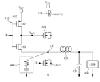
도 1을 참조하면, 일반적인 하이 사이드(high side) 엔 채널 스위칭 벅 컨버터(switching buck converter)의 회로 블록이 나타나 있다. Referring to Figure 1, a circuit block of a typical high side channel switching buck converter is shown.
컨버팅 회로는 구동 전원(VPOW)과 접지(Vss)간에 차례로 연결된 엔 채널(p-channel) 파워 스위치(420)와 엔 채널(n-channel) 스위치(421)를 포함한다. The converting circuit includes a p-
또한, 상기 컨버팅 회로는 피 채널 트랜지스터(412)와 엔 채널 트랜지스터(413)로 이루어진 게이트 드라이버(410)를 포함한다. 상기 게이트 드라이버(410)의 출력단에는 게이트 전압(VGATE)이 PWM 신호 등과 같은 입력에 응답하여 생성된다. 상기 게이트 드라이버(410)의 상기 게이트 전압(VGATE)은 상기 엔 채널 파워 스위치(420)의 게이트에 인가된다. In addition, the converting circuit includes a
한편, 게이트 전압의 부스팅을 위해 커패시터(430)가 다이오드(416)의 캐소드와 상기 엔 채널 파워 스위치(420)의 스위칭 출력노드(LX)간에 연결되고, 전원 전압(VDD)은 상기 다이오드(416)의 애노드에 연결된다. 스위칭 출력노드(LX)에는 인덕터(434)와 커패시터(431)가 연결될 수 있다. 한편 인덕터(415)는 기생(Parasitic)인덕터이다. A
도 1의 회로 동작이 이하에서 설명된다. The circuit operation of Fig. 1 is described below.
먼저, 엔 채널 파워 스위치(420)는 게이트의 전압(VGATE)이 드레인-소스(drain-source)의 전압보다 문턱전압(VTH)만큼 높은 전압일 때 스위칭 온(switching ON)이 된다. 즉 하이 사이드(high side) 엔 채널 파워 스위치(420)가 스위칭 온되는 경우에는 엔 채널 파워 스위치(420)의 게이트 전압(VGATE)이 상기 구동 전원(VPOW)의 전압보다 높아야 한다. 그러므로 엔 채널 파워 스위치(420)의 게이트 전압(VGATE)은 도 2의 파형 WF2와 같이 부트스트랩(bootstrap) 동작에 따라 상기 구동 전원(VPOW)의 전압보다 높게 상승된다. First, the
도 2의 신호 파형도에서 가로축은 시간을 나타내고 세로축은 전압 또는 전류 레벨을 가리킨다. In the signal waveform diagram of FIG. 2, the horizontal axis indicates time and the vertical axis indicates voltage or current level.
신호 파형 WF1은 도 1의 회로에 인가되는 입력 예를 들어 PWM 신호의 파형을 나타내고, 신호 파형 WF2은 상기 엔 채널 파워 스위치(420)의 게이트 전압(VGATE)과 엔 채널 파워 스위치(420)의 스위칭 출력노드(LX)의 출력 전압(VLX)을 함께 나타낸다. 또한 신호 파형 WF3은 스위칭 출력노드(LX)의 인덕터(434)의 전류(IL)와 부하 전류(ILOAD)를 함께 나타내고, 신호 파형 WF4는 상기 엔 채널 파워 스위치(420)의 스위칭 동작에 의해 발생되는 스위칭 전류를 나타낸다.The signal waveform WF1 represents the waveform of the PWM signal applied to the circuit of FIG. 1, for example, and the signal waveform WF2 represents the waveform of the gate voltage (V GATE ) of the yen
하이 사이드 엔 채널 파워 스위치(420)가 오프(OFF)인 경우에 스위칭 출력노드(LX)의 전압은 이상적(ideal)인 조건에서는 그라운드(Ground)로 설정되고, 도 1의 커패시터(430)의 전압(CBST)은 전원전압에서 다이오드(416)의 전압이 감해진 전압, 즉 VDD-VDIODE 만큼으로 차아지(charge)된다.The voltage of the switching output node LX is set to ground at an ideal condition when the high side
시점 t0에서 상기 PWM 신호가 하이 펄스로 인가되면, 상기 게이트 전압(VGATE)은 게이트 드라이버(410)에 의해 상승하기 시작한다. 상기 게이트 전압(VGATE)의 상승에 의해 상기 엔 채널 파워 스위치(420)가 턴온되면 스위칭 출력노드(LX)의 전압(VLX)이 도 2의 신호 파형 WF2과 같이 상승하기 시작한다. When the PWM signal is applied as a high pulse at a time point t0, the gate voltage (V GATE ) starts rising by the gate driver (410). When the enchannel
한편, 상기 게이트 드라이버(410)의 엔 채널 트랜지스터(412)의 드레인 전압(VBST)은 그라운드(예를 들어 0볼트)를 기준으로 VLX +"VDD-VDIODE"의 전압레벨로 된다. 여기서, "VDD-VDIODE"는 상기 커패시터(430)의 프리차아지 전압(CBST)이다. 상기 드레인 전압(VBST)은 상기 스위칭 출력노드(LX)의 전압(VLX)이 상승함에 따라 동반 상승한다. 상기 스위칭 출력노드(LX)의 전압(VLX)은 이상적인 상황에서는 상기 구동 전원의 전압 VPOW까지 상승한다. 이 경우에 게이트 드라이버(410)는 상기 드레인 전압(VBST)을 동작 전원으로서 수신하므로, 부트스트랩된 게이트 전압(VGATE)을 발생한다. 결국, 상기 게이트 전압(VGATE)은 도 2의 신호 파형 WF2에서 보여지는 바와 같이 VDD-VDIODE+VPOW(=VLX)레벨로 부트스트랩(Bootstrap)되어짐을 알 수 있다. On the other hand, the drain voltage V BST of the
도 2의 신호 파형 WF4에서 보여지는 바와 같이 상기 엔 채널 파워 스위치(420)의 스위칭 동작에 의해 발생되는 스위칭 전류(ISW)는 시점 t0에서 급격히 변화된다. 이와 같이 스위칭 온 시점부터 급격하게 변화되는 전류는 회로의 와이어 본딩이나 PCB 레이아웃 디자인(layout design)에서 파생되는 기생 인덕터(415)의 기생 인덕턴스(LPARASITIC)로 인해 전압 스파이크의 발생을 도 3에서와 같이 초래한다. As shown in the signal waveform WF4 in Fig. 2, the switching current I SW generated by the switching operation of the n
도 3은 도 1의 컨버팅 회로에서 기생 인덕턴스의 크기에 따라 나타나는 전압 스파이크의 발생 형태도이다. 3 is a diagram showing the generation of a voltage spike depending on the magnitude of the parasitic inductance in the converting circuit of FIG.
도 3을 참조하면, 인덕턴스의 크기가 서로 다른 기생 인덕터(415,415a,415b)가 상기 엔 채널 파워 스위치(420)의 드레인에 배치된 것이 보여진다. 전압 스파이크의 발생 레벨은 기생 인덕턴스 LPARASITIC 가 클수록, 부하 전류 (Load current) ILOAD가 클수록, 또는 스위칭 슬루 레이트(slew rate) ΔISW이 빠를수록 높아진다. Referring to FIG. 3,
도 3에서 보여지는 출력 전압(VLX)의 파형에서의 전압 스파이크 VSb는 기생 인덕터(415b)의 인덕턴스에 의해 발생된 것이고, 전압 스파이크 VSa는 기생 인덕터(415a)의 인덕턴스에 의해 발생된 것인 바, 전압 스파이크의 발생 레벨은 기생 인덕턴스 LPARASITIC 가 클수록 높음을 알 수 있다. The voltage spike VSb in the waveform of the output voltage VL X shown in Figure 3 is generated by the inductance of the
스위칭 출력노드(LX)의 전압 스파이크(voltage spikes)를 줄일 수 있는 방법 중의 하나는 상기 엔 채널 파워 스위치(420)의 게이트를 드라이브하는 스위칭 슬루 레이트를 최대한 느리게 하는 것이다. 스위칭 슬루 레이트를 가능한한 낮추면 ISW의 순간적인 전류변화량을 최소화 시킬 수 있기 때문이다. One of the ways to reduce the voltage spikes of the switching output node LX is to minimize the switching slew rate driving the gate of the yen
이하에서는 도 1과는 다른 피 채널 파워 스위치와 도 1의 엔 채널 파워 스위치의 스위칭 슬루 레이트에 대한 분석이 설명될 것이다. Hereinafter, the analysis of the switching slew rate of the channel power switch different from that of FIG. 1 and the channel power switch of FIG. 1 will be described.
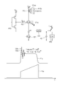
도 4는 도 1의 컨버팅 회로 중 게이트 드라이버와 간단한 피 채널 파워 스위치의 등가회로 및 입출력 전압 파형을 예시적으로 나타낸 도면이다. 또한, 도 5는 도 1의 컨버팅 회로 중 게이트 드라이버와 엔 채널 파워 스위치의 등가회로를 예시적으로 나타낸 도면이다.4 is a diagram illustrating an equivalent circuit and input / output voltage waveforms of a gate driver and a simple to-channel power switch in the converting circuit of FIG. 5 is a diagram illustrating an equivalent circuit of a gate driver and an n-channel power switch in the converting circuit of Fig.
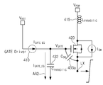
먼저, 도 4를 참조로 일반적이고 간단한 하이 사이드 피 채널 파워 스위치(420P)를 구비한 컨버팅 회로가 설명된다. 설명의 간략화 및 명료화를 위해, 게이트 드라이버(410)는 등가 전류 소오스(equivalent current source)인 IGATE _ EQ로 모델링되고, 피 채널 파워 스위치(420P)는 등가 게이트-소스 커패시터(equivalent gate-source capacitor)인 CSW로 모델링된다. First, referring to FIG. 4, a converting circuit with a common high simple side
파워 스위치가 하이 사이드 피 채널 파워 스위치인 경우에, 도 4의 오른쪽에 나타낸 파형(waveform)처럼, VGATE와 VLX는 VPOW~0V(Ground)사이에서 스윙(swing)한다. 이 경우에 스위칭 슬루 레이트는 IGATE _ EQ/CSW으로서 심플하게 나타남을 알 수 있다. 그러므로 게이트 드라이버의 전류 드라이빙 세기를 적절하게 조절하는 것에 의해 피 채널 파워 스위치인 경우에는 원하는 슬루 레이트를 얻을 수 있다. In the case where the power switch is a high side channelized channel power switch, V GATE and V LX swing between V POW and 0V (Ground), as shown on the right side of FIG. Switching the slew rate in this case, it can be seen that it appears as a simple I GATE _ EQ / C SW. Therefore, by appropriately adjusting the current driving intensity of the gate driver, the desired slew rate can be obtained in case of the channel power switch.
이제 도 5를 참조하면, 도 1의 컨버팅 회로 중 게이트 드라이버(410)와 엔 채널 파워 스위치(420)의 등가회로가 보여진다. Referring now to FIG. 5, an equivalent circuit of the
도 4와 유사하게, 엔 채널 파워 스위치(420)는 등가 게이트-소스 커패시터(equivalent gate-source capacitor)인 CSW로 모델링된다. 상기 등가 커패시터(433a)는 VGATE 와 스위칭 출력 노드(LX)간에 연결되어 있고, VGATE와 그라운드 간에는 기생 커패시턴스를 CPARASITIC 를 갖는 기생 커패시터(432)가 추가로 연결되어 있다. 또한, 게이트 드라이버(410)는 등가 전류 소오스(equivalent current source)인 IGATE _ EQ로 모델링된다. Similar to Fig. 4, the n-
도 5의 동작은 도 6을 통해 구체적으로 설명된다. The operation of FIG. 5 will be described in detail with reference to FIG.
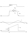
도 6은 도 5에 따른 구간별 입출력 전압 파형과 슬루 레이트에 따른 전압 스파이크의 사이즈를 예시적으로 보여주는 도면이다. FIG. 6 is a diagram illustrating an exemplary input / output voltage waveform according to an interval and a size of a voltage spike according to a slew rate according to FIG.
도 6을 참조하면, 엔 채널 파워 스위치(420)의 스위칭 슬로프 파형이 확대적으로 나타나 있다. Referring to FIG. 6, the switching slope waveform of the yen
도 4의 피 채널 파워 스위치와는 달리, 엔 채널 파워 스위치(420)의 동작 구간은 스위칭 출력 노드(LX)와 VGATE의 부트스트랩 효과로 인해 도 6에서와 같이 3 구간으로 나뉘어 분석될 수 있다. 4, the operation period of the N
제1 구간(T1)에서 스위칭 출력 노드(LX)의 전압 VLX은 리얼 그라운드(real-ground)로 고정되고, VGATE의 전압은 IGATE _ EQ가 CSW를 차아지(charge)함에 의해 상승한다. 상기 VGATE의 전압이 VTHN의 레벨까지 상승하면 상기 엔 채널 파워 스위치(420)가 턴 온(turn-on)된다. The fixed to the first section voltage V LX is a real ground (real-ground) of the switching output node (LX) from the (T1), the voltage of the V GATE is I GATE _ EQ rises By charge (charge) car C SW do. When the voltage of V GATE rises to the level of V THN , the en
제2 구간(T2)에서 상기 엔 채널 파워 스위치(420)가 턴 온됨에 따라, VLX는 VPOW까지 부트스트랩되며, CSW를 통해 VGATE도 VLX와 동일한 슬로프(slope)을 가지고서 함께 상승한다. As the
제3 구간(T3)에서 IGATE _ EQ 는 VGATE를 VBST(=VDD+LX)레벨까지 차아지한다. I claim GATE at 3 intervals (T3) _ EQ is a charge difference V GATE to V BST (= VDD + LX) level.
상기 구간들 중에서 제1 및 제3 구간의 슬루 레이트는 일반적인 피 채널 파워 스위치의 경우와 동일 하다. 그러나, 제2 구간(T2)의 빠른 슬루 레이트는 전압 스파이크에 워스트(worst)한 영향을 준다. The slew rates of the first and third sections of the sections are the same as those of the general channel power switch. However, the fast slew rate of the second section T2 has a worst effect on the voltage spike.
보다 자세한 설명을 위해 각 구간의 슬루 레이트에 대한 분석이 도 7 및 도 8을 참조로 수행된다. For a more detailed description, analysis of the slew rate of each section is performed with reference to FIGS. 7 and 8. FIG.
도 7은 도 6 중 제1,3 구간과 관련하여 도 1의 컨버팅 회로의 간단한 등가 회로 모델을 나타낸 도면이고, 도 8은 도 6 중 제2 구간과 관련하여 도 1의 컨버팅 회로의 간단한 등가 회로 모델을 나타낸 도면이다. FIG. 7 is a diagram showing a simple equivalent circuit model of the converting circuit of FIG. 1 in relation to the first and third sections of FIG. 6, and FIG. 8 is a simplified equivalent circuit diagram of the converting circuit of FIG. 1, Fig.
먼저, 도 7을 참조하면, 제1 구간과 제3 구간에서는 LX node가 각각 AC ground (1구간 = ground, 3구간 = VPOW) 이다. 이때 CSW 는 CPARASISTIC보다 월등히 크므로 스위칭 슬루 레이트는 IGATE _ EQ/(CSW+CPARASITIC)=IGATE _ EQ/CSW로 나타낼 수 있다. 즉, 제1,3 구간에서는 IGATE _ EQ가 화살부호 AR1 같이 CSW로 흐르게 된다. First, referring to FIG. 7, in the first and third sections, the LX node is AC ground (one section = ground, three sections = V POW ). The C SW is the switching slew rate by far greater than the C PARASISTIC can be represented by I GATE _ EQ / (C + C SW PARASITIC) = _ I GATE EQ / C SW. That is, in the range of 1,3 a GATE I _ EQ flows to C SW as arrow sign AR1.
도 8에서는 도 7의 경우와는 달리 제2구간은 스위칭 출력 노드(LX)의 전압 VLX이 부트스트랩되어 플라잉(flying)되는 구간이므로 VGATE에서 CSW로 바라보는 임피던스는 고 임피던스(high impedence)가 된다. 즉, 제2 구간에서는 IGATE _ EQ가 CSW로 흐르지 못하고 화살부호 AR2와 같이 CPARASITIC 로 흐르게 되어, 스위칭 슬루 레이트는 IGATE_EQ/CPARASITIC 으로 된다. 따라서, 슬루 레이트는 급격히 증가하게 된다. 8, the second section is a section where the voltage V LX of the switching output node LX is bootstrapped and flying, so that the impedance viewed from V GATE to C SW is high impedance ). That is, in the second section does not flow to the GATE I _ EQ is C SW flows to C PARASITIC as an arrow AR2 code, switching the slew rate is to GATE_EQ I / C PARASITIC. Therefore, the slew rate is rapidly increased.
정리하면, 스위칭 슬로프 슬루 레이트(제1,3구간)= IGATE _ EQ/CSW가 되고, 스위칭 슬로프 슬루 레이트(제2구간)= IGATE _ EQ/CPARASITIC가 된다. 여기서 제2 구간의 높은 슬루 레이트는 LX node의 큰 전압 스파이크(large voltage spikes)발생의 주원인으로 작용한다.In short, and the switching slopes of the slew rate (the
스위칭 출력 노드(LX)에서 발생되는 전압 스파이크를 줄이는 일반적인 방법으로서 도 7,8에서 보여지는 IGATE _ EQ를 줄여 슬루 레이트를 낮추는 방법이 흔히 사용되어왔다. 그러나 이러한 방법에서의 문제는 파워 로스를 유발한다는 것이다. 즉, 제2 구간의 슬루 레이트를 기준으로 IGATE _ EQ를 낮추면 제1,3 구간의 스위칭 슬로프도 함께 낮아지므로, 매우 큰 파워 로스(power loss)가 발생될 수 있다. As a general method of reducing the voltage spike generated by the switching output node (LX) by lowering the slew rate by reducing the GATE I _ EQ shown in Figure 7 and 8 it has been commonly used. However, the problem with this method is that it causes power loss. That is, is lowered with the slope of the road switching 1,3 interval I decreasing the GATE _ EQ relative to the slew rate of the second zone, a very large power loss (power loss) can be generated.
또한, IGATE _ EQ를 CPARASITIC에 맞추어 설계한다고 하여도 외부의 와이어본딩 등에의해 기인되는 LPARASITIC의 양을 정확히 예측하기 어렵다. 그러므로 적절한 스위칭 슬루 레이트를 얻기 위해 IGATE _ EQ값을 구하는 데 또 다른 어려움이 있다. 결국, LPARASITIC 값이 오버 추정(over estimate)되어 슬루 레이트가 필요 이상으로 느리게 되면 그 만큼 스위치 컨턱션 파워 로스(switch conduction power loss)가 발생된다. 반대로 LPARASITIC 값이 언더 추정(under estimate)되어 슬루 레이트가 적정 수준보다 빠르게 되면 전압 스파이크를 제대로 제한하기 어렵다. In addition, I GATE _ and that the EQ designed for the C PARASITIC also difficult to accurately predict the amount of L PARASITIC be caused by external wire bonding. Therefore, there is another difficulty to obtain the I GATE _ EQ value to obtain a proper switching slew rates. As a result, if the L PARASITIC value is over estimated and the slew rate becomes slower than necessary, a switch conduction power loss is generated accordingly. Conversely, if the L PARASITIC value is under estimate and the slew rate is faster than the proper level, it is difficult to properly limit the voltage spike.
위와 같은 단점을 개선하기 위해 도 9에서 보여지는 바와 같이 복수의 선택 모드를 갖는 게이트 드라이버가 컨버팅 회로에 채용될 수 있다. In order to overcome such disadvantages, a gate driver having a plurality of selection modes as shown in Fig. 9 may be employed in the converting circuit.
도 9는 도 1의 컨버팅 회로에서 게이트 드라이버를 모드 체인징 게이트 드라이버로 변형한 회로를 나타내는 도면이다. 9 is a circuit diagram showing a circuit in which the gate driver is changed to a mode changing gate driver in the converting circuit of FIG.
도 9를 참조하면, 게이트 드라이버(410)는 복수의 선택 모드에 따라 드라이빙 동작을 수행할 수 있다. 모드 첸지(change) 비트를 입력하는 것에 의해 게이트 드라이버(410)의 구동 용량이 가변된다. 예를 들어, 모드 첸지 비트(mode change bit)을 바꾸어 주면 IGATE _ EQ는 0.5X에서 3.5X까지 바뀔 수 있다. 전압 스파이크의 실장 측정값을 비교함에 의해 디자이너(designer)는 가장 적절한 값으로 상기 모드 첸지 비트의 값을 선택할 수 있다. Referring to FIG. 9, the
도 9의 게이트 드라이버의 구동 능력을 모드 첸지 비트를 이용하여 선택하는 테크닉은 크게 두 가지의 단점을 가진다. The technique of selecting the driving capability of the gate driver of FIG. 9 using the mode cyan bit has two disadvantages.
첫 번째로, 게이트 드라이버의 적정 구동값을 만들기 위해 사용되어지는 트랜지스터 이외에, 사용되어지지 않는 트랜지스터는 실리콘 면적(silicon area)을 낭비(waste)하게 된다. 두 번째로, 게이트 드라이버의 사이즈는 한정된 스텝(step)만큼으로 변화되기 때문에 최적 스위칭 슬루 레이트 포인트(optimum switching slew rate point)를 찾기 어렵다. First, in addition to the transistors used to produce the appropriate drive values for the gate drivers, unused transistors waste the silicon area. Secondly, since the size of the gate driver varies by a limited number of steps, it is difficult to find an optimum switching slew rate point.
또한, 도 9를 이용하는 기술은 하나의 고정 스위칭 슬루 레이트(fixed switching slew rate)로 선택되므로 다양한 부하 전류 상황과 어플리케이션 보드 환경을 적절히 커버(cover)하기 어렵다. 예를 들어, 헤비 로드 전류(heavy load current)상황에서 발생되는 비교적 큰 전압 스파이크 수준에 맞추어 스위칭 슬루 레이트가 낮게 설정된 경우라면, 모든 구간에서 전압 스파이크가 제한되는 효과를 가져온다. 그러나 라이트 내지 중 부하 전류(light-to-medium load current)상황에서는 슬루 레이트가 필요 이상으로 낮아진 결과가 되므로, 보다 큰 파워 로스를 유발한다. 따라서, 파워 효율(power efficiency)이 저하된다. In addition, since the technique using FIG. 9 is selected with one fixed switching slew rate, it is difficult to adequately cover various load current situations and application board environments. For example, if the switching slew rate is set to a relatively high voltage spike level that occurs in a heavy load current situation, the voltage spike will be limited at all intervals. However, in a light to medium load current situation, the slew rate becomes lower than necessary, resulting in a larger power loss. Therefore, the power efficiency is lowered.
또 다른 예로서, 하나의 어플리케이션 보드 환경에 따라 스위칭 슬루 레이트를 적정하게 설정하여 전압 스파이크를 제한할 경우에도, 다른 어플리케이션 보드나 보드 상의 인덕턴스(inductance) 편차에 의해 여전히 전압 스파이크가 적절히 제한되지 않을 수 있다. 따라서 이러한 문제를 해결하기 위해 슬루 레이트를 더 낮게 조절하는 것은 그 마진(margin)만큼 파워 로스가 유발된다. As another example, even if the switching slew rate is appropriately set to limit the voltage spike according to one application board environment, the voltage spike may still not be appropriately limited due to inductance deviation on another application board or board have. Therefore, lowering the slew rate to solve this problem causes a power loss as much as the margin.
전압 스파이크를 줄이는 다른 방법으로서는 도 10과 같이 회로 내에 스누버 (snubber circuit)회로를 적용하는 방법도 있다. As another method of reducing the voltage spike, there is a method of applying a snubber circuit circuit in the circuit as shown in Fig.
도 10은 도 1의 컨버팅 회로에서 스누버 회로를 추가한 회로를 나타내는 도면이다. 10 is a diagram showing a circuit in which the snubber circuit is added in the converting circuit of FIG.
도 10을 참조하면, 스위칭 출력노드(LX)와 그라운드 간에 스누버 회로(440)가 설치된 예가 보여진다. 10, an example in which the
스누버 회로(440)의 채용에 의해, 스위칭 출력노드(LX)의 과도 전압 스파이크(excessive voltage spikes)가 효과적으로 댐프(damped)되지만, 그만큼의 파워가 불필요하게 소모되어, 파워 효율이(efficiency)은 떨어지는 단점이 있다. 또한, 이외에도 외부 소자들을 추가로 설치하는 것에 의해 비용이나 면적소모의 단점이 발생된다. The excessive voltage spikes of the switching output node LX are effectively damped by the use of the
상술한 바와 같이 파워 스위치의 스위칭 슬루 레이트를 느리게 제어하여 전압 스파이크를 제한하는 일반적인 방법은, 전압 스파이크로 인해 발생되는 문제들, 예를 들면, EMI 노이즈, 내부 소자의 디메지(damage), 다이나믹 파워 로스(dynamic power loss), 또는 노이즈로 인한 레귤레이터 콘트롤러의 오동작을 방지하거나 줄인다. 그러나, 슬루 레이트를 고정된 슬루 레이트에 맞춰 느리게 하는 것은 스위치 컨덕션 파워 로스(switch conduction power loss)를 더 크게 하는 현상을 유발한다. 또한, 위와 같은 일반적인 방법은 어플리케이션 보드 환경에 따라 전압 스파이크가 다르게 나타나는 현상을 완벽히 제어하기 어렵다. As described above, a general method of slowly controlling the switching slew rate of the power switch to limit voltage spikes is to reduce problems caused by voltage spikes, such as EMI noise, internal device damage, dynamic power Prevents or reduces malfunction of the regulator controller due to dynamic power loss or noise. However, slowing down the slew rate to a fixed slew rate results in a larger switch conduction power loss. In addition, it is difficult to completely control the phenomenon that the voltage spike is different depending on the application board environment.
따라서, 모든 어플리케이션 보드(application boards)상황에서 동일한 전압 스파이크 억제 성능을 실현하는 장치가 필요해진다. 본 발명의 개념에 따른 실시 예에서는 스위칭 시 발생되는 전압 스파이크를 적응적으로 제어할 수 있는 어댑티브 전원 컨버팅 장치가 도 11과 같이 제공된다.Therefore, a device that realizes the same voltage spike suppression performance in all application board situations is needed. In an embodiment according to the concept of the present invention, an adaptive power converter capable of adaptively controlling voltage spikes generated in switching is provided as shown in FIG.
이제부터 본 발명의 개념에 따른 실시 예가 설명된다. Embodiments according to the concept of the present invention will now be described.
도 11은 본 발명의 개념적 실시 예에 따른 전원 컨버팅 장치의 블록도이다. 11 is a block diagram of a power conversion device according to a conceptual embodiment of the present invention.
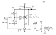
도 11을 참조하면, 전원 컨버팅 장치는, 컨버팅 회로(400)와 슬루 리미터(300)를 포함한다. Referring to FIG. 11, the power converting apparatus includes a converting
상기 컨버팅 회로(400)는 게이트로 인가되는 입력에 따라 구동 전원전압(VPOW)을 구동하여 스위칭 출력노드(LX)로 인가하는 파워 스위치(420)를 포함한다. The converting
상기 슬루 리미터(300)는 상기 파워 스위치(420)의 상기 게이트와 그라운드 간에 연결되어 상기 스위칭 출력노드의 출력 전압에서 나타나는 전압 스파이크의 사이즈를 줄이면서도 파워 효율을 증가시키기 위해 상기 출력 전압의 슬루 레이트를 조절한다. The
상기 슬루 리미터(300)는 도 12에서 보여지는 바와 같이 상기 파워 스위치(420)의 게이트-소스 커패시턴스(433a)에 비해 작은 커패시턴스를 갖는 커패시터(CSL)일 수 있다. The
도 11에서의 경우, 전원 컨버팅 장치는, 상기 파워 스위치의 상기 게이트와 상기 슬루 리미터 간에 연결되어 상기 슬루 리미터를 통해 흐르는 전류를 부하 변동에 따라 적응적으로 조절하는 슬루 레이트 콘트롤러(200)를 더 포함할 수 있다. 11, the power converting apparatus further includes a
상기 슬루 레이트 콘트롤러는 도 14에서 보여지는 바와 같이 제어전압 신호(VCTRL)에 따라 저항값이 가변되는 가변저항으로서 기능하는 모스 트랜지스터(200)일 수 있다. The slew rate controller may be a
도 11에서의 경우, 전원 컨버팅 장치는, 상기 스위칭 출력노드의 출력 전압을 모니터링하여 상기 제어전압 신호를 생성하는 어댑티브 스위칭 콘트롤러(100)를 더 포함할 수 있다. 11, the power conversion apparatus may further include an
상기 어댑티브 스위칭 콘트롤러(100)는, 도 15에서 보여지는 바와 같이 제1 동작구간에서 인가되는 상기 스위칭 출력노드의 출력 전압을 샘플링 및 홀드하는 샘플 앤드 홀드 회로(110), 상기 제1 동작구간의 다음 구간인 제2 동작구간에서 인가되는 상기 스위칭 출력노드의 출력 전압을 상기 샘플 앤드 홀드 회로의 출력과 비교하여 전압 스파이크 검출의 유무를 가리키는 비교 신호를 출력하는 비교기(120), 및 상기 비교 신호의 레벨에 따라 슬루 레이트 조절을 위해 차징 업 또는 디스차아징되는 전압을 생성하여 상기 제어전압 신호로서 출력하는 인터그레이터(130)를 포함할 수 있다. 15, the
상기 인터그레이터(130)의 디스차아징 경로에는 도 17에서 보여지는 바와 같이 역류 방지 기능을 위한 다이오드(143)가 추가적으로 설치될 수 있다. As shown in FIG. 17, a diode 143 for a reverse current blocking function may be additionally installed in the dischaging path of the
상기 샘플 앤드 홀드 회로(110)는 샘플링된 상기 스위칭 출력노드의 출력 전압을 홀드 시에 도 16에서 보여지는 바와 같이 전압 스파이크의 허용 설계 값인 문턱전압 값(VTH)을 상기 샘플링된 출력 전압에 더하여 홀드할 수 있다. The sample and hold
도 11에서 상기 슬루 리미터(300)는 엔 채널의 파워 스위치(420)를 갖는 컨버팅 회로(400)에서, 부트스트랩 구간에서의 슬루 레이트가 급격히 올라가는 문제를 파워 효율을 크게 저하시키지 않으면서 해소하는 역할을 한다. 11, the
상기 슬루 레이트 콘트롤러(200)는 일반적인 고정 스위칭 슬루 레이트(fixed switching slew rate)의 제어 기법과는 달리, 스위칭 슬루 레이트가 환경이나 부하변동에 따라 적응적으로 변화되도록 하는 역할을 한다. Unlike a general fixed switching slew rate control technique, the
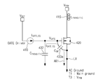
도 12는 도 11중 슬루 리미터가 컨버팅 회로에 연결된 세부 구성을 보여주는 회로도이다. 12 is a circuit diagram showing a detailed configuration in which a slew limiter in Fig. 11 is connected to a converting circuit; Fig.
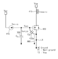
도 12를 참조하면, 슬루 리미터(200)는 VGATE와 그라운드 사이에 연결된 slew-limiting capacitor(CSL)로써 구현된다. 여기서, 상기 CSL의 커패시턴스는 CSW의커패시턴스 보다 상대적으로 작은 값으로 설정된다. Referring to FIG. 12, the
상기 슬루 리미터(200)의 설치에 의해, 도 6에서의 제1,2,3 구간들의 스위칭 슬루 레이트가 파워 효율은 높으면서도 전압 스파이크는 감소되도록 제어된다. 즉, 제2 구간의 높은 슬루 레이트는 감소되도록 하여 전압 스파이크 현상을 줄이는 반면, 제1,3 구간의 슬루 레이트는 증가되도록 하여 파워 로스가 도미넌트(dominant)한 부하 전류 영역에서의 파워 효율을 높인다. 이러한 효과는 도 13a, 13b에서 구체적으로 설명된다. By the installation of the
도 13a는 도 6 중 제1,3 구간과 관련하여 도 12에 따른 회로의 간단한 등가 회로 모델을 나타낸다. 또한, 도 13b는 도 6 중 제2 구간과 관련하여 도 12에 따른 회로의 간단한 등가 회로 모델을 나타낸다. Fig. 13A shows a simple equivalent circuit model of the circuit according to Fig. 12 in relation to the first and third sections of Fig. Fig. 13B shows a simple equivalent circuit model of the circuit according to Fig. 12 in relation to the second section of Fig.
먼저 도 13b를 참조하면, 제2 구간에서는 CSW의 네거티브 노드(negative node)인 스위칭 출력 노드(LX)의 전압은 부트스트랩핑되어 급격히 증가되므로, 스위칭 출력 노드(LX)는 AC상 고 임피던스 노드(high impedance node)로 된다. 그러므로 게이트 드라이버(410)에서 보이는 유효 커패시턴스(effective capacitance)는 CSL이 된다. 즉, IGATE _ EQ는 화살부호 AR20을 따라 흐른다. 따라서, 제2 구간(T2)에서의 스위칭 슬루 레이트는 IGATE _ EQ/CSL이 된다. 이에 비해, 도 8의 경우에는 IGATE_EQ/CPARASITIC 이었다. CSL 은 CPARASITIC보다 월등히 크므로(CPARASITIC << CSL), 도 12와 같은 회로의 경우에 제2 구간의 스위칭 슬루 레이트는 도 8에 비해 상대적으로 느리게 제어되는 것을 알 수 있다. Referring to FIG. 13B, in the second period, the voltage of the switching output node LX, which is a negative node of C SW , is suddenly increased due to bootstrapping, so that the switching output node LX is connected to the AC high- (high impedance node). Therefore, the effective capacitance seen at the
이와 같이 제2 구간에서의 스위칭 슬루 레이트는 느리게 조절되나, 파워 효율에 더 큰 영향력을 가지는 제1,3 구간에서는 상대적으로 더 빠른 스위칭 슬루 레이트를 갖는다. Thus, the switching slew rate in the second section is adjusted slowly, but has a relatively faster switching slew rate in the first and third sections having greater power efficiency.
도 13a를 참조하면, 제1,3 구간에서 CSW의 네거티브 노드인 스위칭 출력 노드(LX)는 AC 그라운드이다. 제1 구간에서는 리얼 그라운드이고, 제3 구간에서는 VPOW가 된다. 그러므로 게이트 드라이버(410)에서 보이는 유효 커패시턴스는 CSW+CSL가 된다. 따라서, 이 경우에 스위칭 슬루 레이트는 IGATE _ EQ/(CSW+CSL)이 된다. Referring to FIG. 13A, the switching output node LX, which is a negative node of C SW in the first and third periods, is AC ground. In the first section, it is a real ground, and in the third section is V POW . Therefore, the effective capacitance seen by the
여기서, CSL << CSW이므로, 도 13a에서의 제1,3 구간 스위칭 슬루 레이트는 IGATE_EQ/CSW이 된다. Here, since C SL << C SW , the first and third section switching slew rate in FIG. 13A becomes I GATE_EQ / C SW .
이를 도 7의 경우와 비교 시, 제1,3 구간 스위칭 슬루 레이트가 IGATE _ EQ(일반 기술)/CSW으로서 나타나는 도 7과 동일하게 됨을 알 수 있다. 그러나 제2 구간의 CSL 이 CPARASITIC 보다 큰 만큼 상기 IGATE _ EQ를 도 13a의 경우에는 도 7의 경우에 비해 더 크게 설계하기 때문에, 제1,3 구간에서의 스위칭 슬루 레이트는 도 7의 경우에 비해 빠르게 된다. 즉, IGATE _ EQ(도 13a 케이스) >> IGATE _ EQ(도 7 케이스)이므로, 결과적으로 전체 파워 효율(overall power efficiency)은 높아진다. It can be seen that even when compared with the case of 7, the 1,3 period switching slew rates in the same manner as in Figure 7 appears as I _ GATE EQ (General techniques) / C SW. However, due to the larger design than the much larger than the second leg of the C SL C PARASITIC For the GATE I _ For the EQ Figure 13a In Figure 7, the switching slew rate in the interval of 1, 3 7 Compared to the case. That is, I GATE _ Since EQ (Figure 13a case) >> I GATE _ EQ (7 cases), as a result, overall power efficiency (overall power efficiency) is high.
상기한 이점에도 불구하고 도 12의 회로는 아래와 같은 구조적 단점을 가질 수 있다. Despite the above advantages, the circuit of FIG. 12 may have the following structural drawbacks.
도 12에서의 CSL은 다이나믹 파워 로스(dynamic power loss)를 증가시킬 수 있으므로 완전 라이트 부하 조건(extreme light load condition)에서 파워 효율을 저하시킬 수 있다. 늘어나는 다이나믹 로스는 다음과 같이 나타낼 수 있다. The C SL in FIG. 12 can increase the dynamic power loss and therefore lower the power efficiency in an extreme light load condition. The increasing dynamic loss can be expressed as follows.
즉, 일반 기술에서의 다이나믹 로스는, PDYNAMIC(일반 기술)=CSW x VDD2 x fS 이고, 도 12에서의 다이나믹 로스는, PDYNAMIC(도 12 케이스)= CSW x VDD2 x fS + CSL x VBST 2 x fS 으로 나타난다. 결국, CSL x VBST 2 x fS 만큼의 부가적 파워 로스(additional power loss)가 발생되는 것이다. That is, the dynamic loss in the general technology is P DYNAMIC (general technology) = C SW x VDD 2 xf S , And the dynamic loss in Fig. 12 is P DYNAMIC (case in Fig. 12) = C SW x VDD 2 xf S + C SL x V BST 2 xf S . Finally, C SL x V BST 2 xf S An additional power loss is generated.
또 다른 단점은 적절한 CSL값을 찾는 어려움이다. CSL이 너무 크게 설계된다면, 각 구간에서의 슬루 레이트의 감소로 컨덕션 파워 로스가 일어나며, CSL이 너무 작게 설계된다면 전압 스파이크를 적절히 제어할 수 없게 된다. Another disadvantage is the difficulty of finding an appropriate C SL value. If C SL is designed too large, the reduction of the slew rate in each section will result in a conducive power loss, and if the C SL is designed too small, the voltage spike will not be properly controlled.
그러나, 전압 스파이크의 특성이 부하 전류의 양에 따라, 그리고 외부 와이어 본딩과 PCB 레이아웃에서 생성되는 LPARASITIC값에 따라, 크게 변하기 때문에 이 이상적인 CSL 값은 각 상황에 따라 변하게 되고 정확히 예측하기도 어렵다. However, since the characteristics of voltage spikes vary greatly with the amount of load current and with the L PARASITIC value generated in the external wire bonding and PCB layout, this ideal C SL value varies with each situation and is difficult to predict accurately.
따라서, 위와 같은 도 12의 회로는 제2 구간의 슬루 레이트를 낮추어, 엔 채널 파워 스위치 타입에서 문제시되었던 전압 스파이크문제를 해결한다. 동시에 도 12의 회로는 제1,3 구간의 슬루 레이트를 증가시킴에 의해 컨덕션 파워 로스가 도미넌트(dominant)한 부하 전류 영역에서 파워 효율을 높인다. Therefore, the circuit of Fig. 12 as described above lowers the slew rate of the second section, thereby solving the voltage spike problem which has been a problem in the yen channel power switch type. At the same time, the circuit of FIG. 12 increases the slew rate of the first and third sections, thereby increasing the power efficiency in the load current region dominated by the conduction power loss.
그러나, 완전 라이트 부하 조건에서는 CSL로 인한 다이나믹 파워 로스로 인해 파워 효율이 저하되는 단점이 존재하며, 다양한 상황에 맞추어 적절한 CSL값을 설계하는 것도 어려울 수 있다. However, there is a disadvantage in that the power efficiency is lowered due to the dynamic power loss due to the C SL under the full light load condition, and it may be difficult to design an appropriate C SL value for various situations.
위와 같이 도 12의 회로가 갖는 단점들을 해결하기 위해 제2 실시 예로서 의 회로가 도 14에 나타나 있다. A circuit as a second embodiment is shown in Fig. 14 to solve the disadvantages of the circuit of Fig. 12 as described above.
도 14는 도 11중 슬루 레이트 콘트롤러가 컨버팅 회로에 연결된 세부 구성을 보여준다. Fig. 14 shows a detailed configuration in which the slew rate controller in Fig. 11 is connected to the converting circuit.
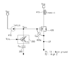
도 14를 참조하면, 슬루 레이트 콘트롤러(200)는 VGATE와 상기 슬루 리미터(200) 사이에 연결된다. 상기한 구성에 따라, 도 14의 회로는 가변저항(variable resistor) RCTRL 을 가지고서 어댑티브(adaptive) 스위칭 슬루 레이트 제어를 행하는 구조를 갖는다. 즉, 도 14는 도 12의 회로 구조에서 슬루 레이트 콘트롤러(200)가 추가된 구조이다. Referring to FIG. 14, the
CSL과 함께 RCTRLL을 시리즈(series)로 연결한 경우에 RCTRL을 통해 CSL 로 흐르는 전류가 조절되므로, 스위칭 슬루 레이트을 원하는 대로 제어할 수 있다. Because current is flowing through the control C SL through R CTRL in the case where R CTRLL with C SL connected in series (series), the switching slew reyiteueul can be controlled as desired.
도 14에서, 상기 RCTRL은 VCTRL의 포텐셜 레벨(potential level)에 따라 0~무한대의 저항값으로 가변될 수 있다. 상기 RCTRL의 저항값을 이용하여 CSL를 차아지하는 IGATE _ EQ의 값을 조절하면, 가변(variable) 스위칭 슬루 레이트가 구현된다. In FIG. 14, R CTRL may vary from 0 to infinite resistance according to the potential level of V CTRL . By adjusting the value of the GATE I _ EQ to charge the car C SL by using a resistance value of the R CTRL, are implemented a variable (variable) switching slew rates.
RCTRL의 저항값을 높이면 스위칭 슬루 레이트가 높아지며, RCTRL의 저항값을 낮추면 스위칭 슬루 레이트가 감소한다. 따라서, RCTRL의 저항값을 0으로 만들어 최소 스위칭 슬루 레이트을 갖도록 하는 것에서부터 시작하여 RCTRL의 저항값을 무한대로 올려 CSL의 슬루 리미터(slew limiter)의 기능을 완전히 없애는 것까지의 제어가 가능할 수 있다. 상기 RCTRL의 저항값을 조절하는 것은 도 15를 통해 설명될 것이다. Increasing the resistance value of R CTRL increases the switching slew rate, and decreasing the resistance value of R CTRL decreases the switching slew rate. Therefore, starting from having the resistance value of R CTRL set to zero to have the minimum switching slew rate, it is possible to control the resistance value of R CTRL to infinity to completely eliminate the function of the C SL 's slew limiter . The adjustment of the resistance value of R CTRL will be described with reference to FIG.
도 14에서, 부하 전류가 커질수록 전압 스파이크는 크게 발생된다. In Fig. 14, the larger the load current, the larger the voltage spike occurs.
일반적인 기술의 경우에 최대 부하 전류(maximum load current)상황에 맞추어 슬루 레이트를 낮게 고정하면, 중간 부하 전류 랜지(load current range)에서는 스위칭 슬루 레이트가 필요이상으로 감소된 상태가 된다. 따라서, 이 경우에는 파워 로스가 발생하게 된다. 반대로 낮은 중간 부하 전류 랜지에 맞추어 슬루 레이트를 높게 설정하면, 파워 로스는 줄일 수 있지만 부하 전류의 상승에 기인하여 전압 스파이크 발생이 커진다. If the slew rate is fixed low for a typical maximum load current situation, then the switching slew rate is reduced beyond the required midrange load current range. Therefore, in this case, a power loss occurs. On the contrary, if the slew rate is set to a high value in accordance with the low intermediate load current range, the power loss can be reduced, but the voltage spike is increased due to the increase of the load current.
따라서, 도 14에서 VCTRL 전압을 바꾸어 RCTRL의 저항값을 조절하는 것이 필요하다. 즉, 스위칭 슬루 레이트 제어를 부하 전류의 상황에 따라, 어플리케이션 보드가 갖는 인덕턴스에 의해 각기 다르게 발생되는 전압 스파이크의 수준에 따라 어댑티브하게 제어하는 것이 필요해진다. 상대적으로 빠른 스위칭 슬루 레이트는 어플리케이션 보드내에서 레스 로드 전류(less load current)나 레스 인덕턴스(less inductance)의 경우에 설정된다. 반대로, 상대적으로 느린 스위칭 슬루 레이트는 어플리케이션 보드내에서 모어 로드 전류(more load current)나 모어 인덕턴스(more inductance)의 경우에 설정된다. 슬루 레이트를 각종 변동 상황에 따라 어댑티브하게 제어하면 파워 효율이 전 영역에서 최대화된다. Therefore, it is necessary to change the V CTRL voltage in FIG. 14 to adjust the resistance value of R CTRL . That is, it is necessary to adaptively control the switching slew rate control according to the level of the voltage spike that is generated differently depending on the inductance of the application board depending on the situation of the load current. A relatively fast switching slew rate is set in the case of less load current or less inductance in the application board. Conversely, a relatively slow switching slew rate is set in the case of more load current or more inductance in the application board. When the slew rate is controlled adaptively according to various change situations, the power efficiency is maximized in the entire region.
이하에서는 도 15를 참조로, 피드백 루프구조를 가지고, 스위칭 슬루 레이트를 어댑티브하게 제어하는 것이 설명될 것이다. Hereinafter, with reference to FIG. 15, it will be described how to adaptively control the switching slew rate with a feedback loop structure.
도 15는 도 11의 전원 컨버팅 장치의 예시적 구체회로도이고, 도 16은 도 15에 따른 적응적 전압 스파이크 조절의 동작 파형도이다. FIG. 15 is an exemplary specific circuit diagram of the power conversion apparatus of FIG. 11, and FIG. 16 is an operational waveform diagram of adaptive voltage spike adjustment according to FIG.
먼저, 도 15를 참조하면, 상기 슬루 레이트 콘트롤러(200)를 제어하기 위해, 상기 스위칭 출력노드(LX)의 출력 전압을 모니터링하여 제어전압 신호(VCTRL)를 생성하는 어댑티브 스위칭 콘트롤러(100)의 세부 구성이 나타나 있다. 15, an
상기 어댑티브 스위칭 콘트롤러(100)는, 샘플 앤드 홀드 회로(110), 비교기(120), 및 인터그레이터(130)를 포함한다. The
상기 어댑티브 스위칭 콘트롤러(100)는 부하 전류와 어플리케이션 보드의 상황에 따라 다르게 발생되는 스위칭 전압 스파이크 수준을 디자인 한계값 이하로 제어하는 동시에 최대 스위칭 슬루 레이트가 얻어지도록 한다. The
먼저, 스위칭 전압 스파이크를 검출하여 상기 제어전압 신호(VCTRL)를 적절하게 생성하는 것에 관한 설명부터 이하에서 개시된다. Firstly, a description will be given hereinafter from the description of detecting the switching voltage spike and appropriately generating the control voltage signal V CTRL .
도 16의 1T구간에서 VLX가 샘플 앤드 홀드 회로(sample & hold circuit :110)로 인가된다. 상기 샘플 앤드 홀드 회로(110)는 상기 제1 동작구간 즉 1T 구간에서 인가되는 상기 스위칭 출력노드(LX)의 출력 전압을 샘플링 및 홀드한다.In the 1T section of FIG. 16, V LX is applied to a sample and hold
이 때 샘플링된 신호 VLX(t-1)는 VLX가 펄스 온(On) 되었을 때의 최종 레벨(전압 스파이크가 사라진 후)에서 전압 스파이크의 설계 마진인 문턱전압 VTH만큼 인 전압 즉, 도 16에서 보여지는 바와 같이 VLX(t-1)+VTH 의 레벨로 홀드된다. At this time, the sampled signal V LX (t-1) is the voltage which is the threshold voltage V TH which is the design margin of the voltage spike at the final level (after the voltage spike disappears) when V LX is pulse on 16, V LX (t-1) + V TH As shown in FIG.
비교기(120)는 상기 제1 동작구간의 다음 구간인 제2 동작구간에서 인가되는 상기 스위칭 출력노드의 출력 전압을 상기 샘플 앤드 홀드 회로(110)의 출력과 비교하여 전압 스파이크 검출의 유무를 가리키는 비교 신호(VCOMP)를 출력한다. 즉, 도 16의 2T 구간이 시작될 때 상기 비교기(120)는 상기 샘플 & 홀드된 상기 VLX(t-1)+VTH와 현재 VLX(2T)의 전압 스파이크를 서로 비교한다. VLX(2T)의 전압 스파이크가 상기 샘플링된 VLX(t-1)+VTH의 레벨을 넘을 때, 전압 스파이크의 발생이 검출된다. 이와 같이 전압 스파이크의 발생이 검출되면, 래치 타입 비교기(latch-type comparator)의 기능을 갖는 상기 비교기(120)는 도 16에서 보여지는 바와 같이 하이 레벨의 비교 신호(VCOMP)를 출력한다. The
상기 제1,2 동작 구간들의 주기는 상기 파워 스위치(420)의 상기 게이트에 인가되는 입력의 주기에 대응될 수 있다. The period of the first and second operating periods may correspond to the period of the input applied to the gate of the
이와 같이 본 실시 예에서의 전압 스파이크 검출 작업은 전압 스파이크가 일어나는 매우 짧은 순간 내에 모두 이루어질 필요가 없다. 즉, 이전 구간에서의 전압 스파이크와 현재 구간에서의 전압 스파이크를 동작 구간 단위로 비교함에 의해 검출의 시간적인 제한을 크게 받지 않는다. 즉, 검출 작업을 위한 고속 회로가 크게 요구되지 않기 때문에 검출의 정확성이 높고, 보다 더 전력효율이 높은 회로의 사용도 가능하게 된다. Thus, the voltage spike detecting operation in this embodiment does not need to be performed within a very short time when a voltage spike occurs. That is, by comparing the voltage spike in the previous section with the voltage spike in the current section in the operation section, the detection time limit is not greatly affected. In other words, since a high-speed circuit for the detection operation is not required to a large extent, it is possible to use a circuit with high detection accuracy and further higher power efficiency.
상기 인터그레이터(130)는 상기 비교 신호(VCOMP)의 레벨에 따라 슬루 레이트 조절을 위해 차징 업 또는 디스차아징되는 전압을 생성하여 상기 제어전압 신호(VCTRL)로서 출력한다. 즉, 상기 인터그레이터(130)는 상기 비교기(120)의 비교 신호인 VCOMP를 수신한다. 상기 인터그레이터(130)는 상기 VCOMP이 하이(HIGH)레벨일 때 VCTRL을 차징 업(charging up)하여 가변 저항 RCTRL의 임피던스(impedence)가 낮아지도록 한다. 이에 따라 현재 구간의 다음 구간에서 스위칭 동작의 슬루 레이트는 낮아진다. 상기 인터그레이터(130)의 차징 업 동작은 전압 스파이크가 원하는 범위를 넘지 않을 때까지 계속 된다. The
도 16의 4T 구간에서는 전압 스파이크가 더 이상 원하는 범위를 넘지 않으므로 VCOMP는 도 16의 4T 구간에서의 파형과 같이 로우(LOW)레벨로 천이된다. 이에 따라 상기 인터그레이터(130)의 차징 업 동작은 끝나고 디스차아징 동작이 시작된다. 즉, 상기 인터그레이터(130)는 VCTRL을 디스차아징한다. 도 16의 (n-1)T 구간에서와 같이, 슬루 레이트가 너무 느려서 전압 스파이크가 VTH보다 필요없이 낮게 발생한다면 상기 인터그레이터(130)는 VCTRL을 디스차아징하여 슬루 레이트를 높인다. Since the voltage spike no longer exceeds the desired range in the 4T interval of FIG. 16, V COMP is changed to the LOW level as shown in the waveform in the 4T interval of FIG. Accordingly, the charging up operation of the
결과적으로 슬루 레이트는 도 16의 nT 구간처럼 전압 스파이크가 VTH바로 아래에 머무는 정도의 크기로 레귤레이트(regulate)된다. As a result, the slew rate is regulated to the extent that the voltage spike stays just below V TH as in the nT section of FIG.
도 15의 회로 구조를 갖는 벅 스위칭 컨버터(buck switching converter)는 어느 변동 상황에서나 전압 스파이크를 VTH 레벨로 제어하여, 최대 스위칭 슬루 레이트를 가질 수 있게 한다. A buck switching converter having the circuit structure of FIG. 15 controls the voltage spike at a V TH level in any variation, allowing it to have a maximum switching slew rate.
더구나, 도 15의 회로 구조는 라이트 부하 조건(light load condition)에서는 슬루 리미터에 의해 추가적인 다이나믹 파워 로스의 단점을 보완한다. 라이트 부하 조건에서는 전압 스파이크가 거의 발생되지 않으므로 상기 어댑티브 스위칭 콘트롤러(100)는 자동으로 상기 RCTRL을 무한대로 올린다. 이에 따라 CSL로 인한 추가적인 다이나믹 파워 로스가 방지된다. Moreover, the circuit structure of FIG. 15 compensates for the disadvantage of additional dynamic power loss by the slew limiter in light load conditions. Under the light load condition, since the voltage spike hardly occurs, the
도 17은 도 15중 인터그레이터의 예시적 구체회로이다. 17 is an exemplary concrete circuit of the integrator in Fig.
도 17을 참조하면, 인터그레이터(130)는 인버터(132), 다이오드(143), 전류원(140), 커패시터(144), 및 복수의 트랜지스터들(133,134,135,136,137,141,142)을 포함한다. 17, the
상기 인터그레이터(130)는 가변저항 RCTRL을 제어한다. RCTRL은 상기 제어전압 신호(VCTRL)의 레벨에 따라 저항 값이 변화된다. 가변저항 RCTRL을 구현하는 방법 중 값싸고 집적하기 쉬운 구현 방법은 CMOS를 사용하는 것이다. 그러나 CMOS를 이용한 가변저항의 구현 방법은, 부트스트랩 구조(Bootstrap structure)에서 어려움을 겪을 수 있다. 그 이유는 CMOS 가변저항인 RCTRL의 드레인 대 소스(Drain to Source) 양단 전압이 매 스위칭 온/오프 구간에서 그라운드 레벨(GND level)부터 LX level(=VPOW Level)까지 변하기 때문이다. 따라서, 도 17에서 상기 RCTRL을 제어하는 VCTRL 전압도 RCTRL의 양단전압이 GND to LX로 변할 때에 맞추어 함께 GND to LX로 변해야 한다. 이를 위해 상기 인터그레이터(130)는 아래와 같이 동작한다.The
상기 비교 신호(VCOMP)의 레벨은 전압 스파이크의 검출 유무에 따라 로우 또는 하이레벨로 된다. 여기서 로우 레벨은 디지털 신호 0이 될 수 있고, 하이 레벨은 디지털 신호 1이 될 수 있다. The level of the comparison signal V COMP becomes low or high level depending on whether voltage spikes are detected or not. Here, the low level may be a
상기 인터그레이터(130)는 상기 비교 신호(VCOMP)의 레벨에 따라 커패시터(144)로서 표시된 CINT를 차아징/디스차아징 시킨다. The
먼저, 스위칭 오프 구간에서는 상기 스위칭 출력 노드(LX)가 GND이기 때문에 일반적인 인터그레이터와 같은 동작을 수행한다. First, since the switching output node LX is at the GND in the switching off period, the switching output node LX performs the same operation as a general inverter.
그러나, 스위칭 온이 되면 상기 스위칭 출력 노드(LX)가 VPOW으로 올라간다. 이 때 CINT는 자동적으로 VCTRL을 VPOW 기준으로 함께 부트스트랩 시킨다. 액추얼(Actual) VCTRL 는 VCTRL + VLX 가 되어 CMOS 가변저항 구조의 RCTRL은 스위칭 오프 때와 같은 저항값으로 고정시킨다. 여기서 다이오드(143)로서 표시된 DINT는 인터그레이터(130)의 차아징 패쓰(charging path)에서 CINT의 역류를 막아 주는 역할을 한다. 또한, 도 17의 인터그레이터(130)의 경우에 디스차아징 패쓰(discharging path)에는 역류 원인 자체를 없애는 구조와 높은 VPOW값에서 신뢰성을 갖기 위해 NLDMOS 미러 구현(mirror implementation)으로 구성되었다. However, when switching on, the switching output node LX rises to V POW . At this time, C INT automatically boots V CTRL together with V POW standard. Actual V CTRL becomes V CTRL + V LX and R CTRL of the CMOS variable resistance structure is fixed to the same resistance value as when switching off. Here, D INT denoted as the diode 143 serves to prevent backflow of C INT in the charging path of the
본 발명의 실시 예에 따른 동작특성 및 이점(benefit)이 도 18 내지 도 20을 통해 이하에서 설명될 것이다. The operating characteristics and benefits according to embodiments of the present invention will be described below through FIGS. 18-20.
도 18은 도 15의 전원 컨버팅 장치에 의해 감소된 전압 스파이크를 대비적으로 보여주는 시뮬레이션 결과 파형도이다. 또한, 도 19는 도 15의 전원 컨버팅 장치에 의한 파워 효율의 변화 추이를 대비적으로 보여주는 시뮬레이션 결과 파형도이고, 도 20은 도 15의 전원 컨버팅 장치에 의한 전압 스파이크의 개선을 부하 전류의 변화에 따라 나타낸 시뮬레이션 결과 파형도이다. FIG. 18 is a waveform diagram of a simulation result showing a voltage spike reduced by the power converter of FIG. 15 in a comparative manner. FIG. FIG. 19 is a waveform diagram of a simulation result showing a change in the power efficiency by the power converting apparatus of FIG. 15, FIG. 20 is a graph showing the improvement of the voltage spike by the power converting apparatus of FIG. And FIG.
첫째로, 하이 사이드 엔 채널 파워 스위치를 포함하는 도 15와 같은 벅 컨버터는 부트스트랩 구간(도 6의 T2 구간에 대응)의 스위칭 슬루 레이트를 낮춘다. 따라서, 스위칭 출력 노드에서 발생되는 전압 스파이크가 전 부하 전류 영역에서 최소화 또는 감소된다. 이러한 동작에 더하여 벅 컨버터는 파워 스위치가 ON/OFF 되는 구간(도 6의 T1 구간, T3 구간)의 스위칭 슬루 레이트를 증가시킨다. 따라서, 컨덕션 파워 로스가 도미넌트한 영역에서 파워 효율이 높아진다. First, a buck converter, such as that of FIG. 15, including a high side channel power switch, lowers the switching slew rate of the bootstrap section (corresponding to the T2 section of FIG. 6). Thus, the voltage spike generated at the switching output node is minimized or reduced in the full load current region. In addition to this operation, the buck converter increases the switching slew rate in the section in which the power switch is turned on / off (T1 section in FIG. 6, T3 section). Therefore, the power efficiency becomes higher in a dominant region of the conduction power loss.
도 18을 참조하면, 그래프 IG1은 도 15의 회로를 통해 전압 스파이크가 제한된 것을 보여준다. 이에 비해 그래프 PG1은 일반적인 벅 컨버터를 통해 나타나는 전압 스파이크가 보여진다. 도 18에서 가로축은 시간을 나타내고 세로축은 전압을 가리킨다. 도 18에서의 시뮬레이션 결과 파형을 대비 시, 제2 구간에서 슬루 레이트를 제어함에 의해 전압 스파이크가 효과적으로 감소되는 것을 확인할 수 있다. Referring to Fig. 18, graph IG1 shows that the voltage spike is limited through the circuit of Fig. Graph PG1, on the other hand, shows the voltage spike seen through a typical buck converter. In Fig. 18, the horizontal axis indicates time and the vertical axis indicates voltage. 18, it can be confirmed that the voltage spike is effectively reduced by controlling the slew rate in the second section.
또한, 도 19를 참조하면, 부하 전류에 따른 파워 효율이 대비적으로 나타나 있다. 도 19에서 가로축은 부하 전류를 나타내고 세로축은 파워 효율을 %로서 가리킨다. 그래프들 중에서 PG 는 일반적인 벅 컨버터를 통해 얻어지는 파워 효율을 보인 것이고, IG 는 도 12의 회로를 통해 얻어지는 파워 효율을 보여준다. 또한, IGI 는 도 14의 회로를 통해 얻어지는 파워 효율을 보인 것이다. Referring to FIG. 19, the power efficiency according to the load current is shown in a comparative manner. In Fig. 19, the abscissa indicates the load current and the ordinate indicates the power efficiency in%. Among the graphs, PG shows the power efficiency obtained with a typical buck converter, and IG shows the power efficiency obtained with the circuit of FIG. The IGI shows the power efficiency obtained through the circuit of Fig.
IGATE_EQ를 극히 낮춘 경우에 나타나는 그래프 PG 를 기준으로 대비할 경우에도 컨덕션 파워 로스가 도미넌트한 100mA~1.5A영역에서 IG 와 IGI 의 경우에 모두 파워 효율이 개선됨을 알 수 있다. 결국, 이는 제1,3 구간에서 슬루 레이트를 빠르게 제어함에 의해 나타나는 효과이다. It can be seen that the power efficiency is improved in both IG and IGI when the conduction power loss is dominant in the range of 100mA ~ 1.5A even when the graph PG shown when the IGATE_EQ is extremely lower is compared. As a result, this is an effect caused by the rapid control of the slew rate in the first and third sections.
둘째로, 라이트 부하 조건(light load condition)에서 슬루 리미터는 추가의 다이나믹 파워 로스를 최소화 또는 줄인다. 라이트 부하 조건에서는 전압 스파이크가 거의 발생되지 않으므로 도 15와 같은 피드백 아키텍쳐(feedback architecture)는 CSL로 인한 추가의 다이나믹 파워 로스를 막기 위해 자동적으로 RCTRL을 무한대로 올린다. 다시 도 19의 그래프 IG 를 참조하면, 슬루 리미터 만의 채용은 다이나믹 파워 로스를 그래프 PG에 비해 증가시킴을 알 수 있다. 즉, 그래프 IG 는 라이트 부하 전류 0~100mA 구간에서 그래프 PG에 비해 파워 효율이 상대적으로 약간 낮다. 그러나, 도 19의 그래프 IG1을 참조 시, 라이트 부하 조건에서도 그래프 PG에 비해 다이나믹 파워 효율이 그다지 저하되지 않음이 확인된다. Second, in light load conditions, the slew limiter minimizes or reduces additional dynamic power losses. Since there is little voltage spike in the light load condition, the feedback architecture as shown in FIG. 15 automatically raises R CTRL to infinity to prevent further dynamic power loss due to C SL . Referring again to the graph IG in FIG. 19, it can be seen that employing only the slew limiter increases the dynamic power loss compared to the graph PG. That is, the graph IG has a relatively low power efficiency compared to the graph PG in the light load current range of 0 to 100 mA. However, referring to the graph IG1 in Fig. 19, it is confirmed that the dynamic power efficiency is not significantly lowered compared to the graph PG even under the write load condition.
셋째로, 전압 스파이크의 사이즈에 따라 최우선적으로 스위칭 슬루 레이트가 조절되기 때문에 와이어본딩 및 PCB 레이아웃 등에서 생성되는 기생 인덕턴스의 다양한 환경에서도 전압 스파이크가 강건(robust)하게 최소화 또는 감소된다. 적응적인 슬루 레이트 조절은 기생 인덕턴스를 정확(accurate)히 예측하는 결과와 마찬가지의 결과를 얻으므로, 도 9와 같이 모드 체인징 게이트 드라이버를 채용할 필요가 없다. 따라서, 그러한 게이트 드라이버를 설치하는 데 따른 불필요한 실리콘 ㅇ에리어어를 줄이므로, 회로가 컴팩트(compact)해지고 구현 비용이 낮아진다. Third, voltage spikes are robustly minimized or reduced even in various environments of parasitic inductance generated in wire bonding and PCB layout, because the switching slew rate is adjusted according to the size of the voltage spike. The adaptive slew rate adjustment results in the same result as the accurate prediction of the parasitic inductance, so there is no need to employ a mode changing gate driver as in FIG. Therefore, since the unnecessary silicon area for installing such a gate driver is reduced, the circuit becomes compact and the implementation cost is lowered.
넷째로, 본 발명의 실시 예에서는 도 16을 통해 설명된 바와 같이 전압 스파이크가 VTH를 넘지 않은 범위 내에서 슬루 레이트가 부하 전류의 양에 따라 항상 최대값을 가질 수 있도록 적응적으로 변한다. 따라서, 최대 부하 전류의 상황에 맞추어 슬루 레이트를 낮게 설계하던 일반 기술이 갖는 문제 즉 파워 로스가 방지 또는 최소화된다. 도 19의 그래프 IG1는 설정된 최대 전류 1.5A 에서는 파워 효율이 그래프 IG와 같고 PG보다 좋다. 상기 최대 전류 1.5A 보다 낮은 부하 전류 영역으로 내려 갈 수록 상기 그래프 IG1의 파워 효율은 그래프 IG보다도 점차로 좋아지는 것이 확인된다. 또한, 도 20을 통해 알 수 있듯이, 모든 상황에서 전압 스파이크는 VTH내로 로버스트(robust)하게 제어된다. 도 20에서 가로축은 시간을 가리키고, 세로축은 각기 표시된 바와 같이 전압 또는 전류를 나타낸다. 도 20에서 가장 상부의 그래프는 일반 기술에서의 스위칭 출력 전압 파형을 나타낸다. 또한 가장 하부의 그래프는 시간에 따라 증가되는 부하 전류를 보여준다. 이와 같이 부하 전류를 증가시킨 경우에 일반 기술에서는 가장 상부의 그래프에서 보여지는 바와 같이 전압 스파이크가 크게 또는 작게 나타난다. 이에 비해 본 발명의 실시 예의 경우에는 가운데 보여지는그래프로서 보여지는 바와 같이 모든 부하 전류 영역에서 전압 스파이크가 설정된 문턱전압 VTH 아래로 제어되는 것이 확실히 나타난다. Fourth, in the embodiment of the present invention, as described with reference to FIG. 16, the slew rate changes adaptively so that the voltage spike does not exceed V TH , so that the slew rate can always have the maximum value according to the amount of the load current. Therefore, the problem of the conventional technique of designing the slew rate low in accordance with the situation of the maximum load current, that is, power loss is prevented or minimized. The graph IG1 of FIG. 19 shows that the power efficiency is the same as the graph IG and is better than the PG at the set maximum current 1.5A. It is confirmed that the power efficiency of the graph IG1 is gradually improved as compared with the graph IG, as it goes down to the load current region lower than the maximum current of 1.5A. In addition, as can be seen from FIG. 20, the voltage spike is robustly controlled to V TH in all situations. 20, the horizontal axis indicates time, and the vertical axis indicates voltage or current as indicated. The uppermost graph in FIG. 20 shows the switching output voltage waveform in the general technology. The bottom graph also shows the load current increased with time. In this way, when the load current is increased, the voltage spike is large or small as shown in the uppermost graph in the general technology. On the contrary, in the case of the embodiment of the present invention, it is clear that the voltage spike is controlled below the set threshold voltage V TH in all the load current regions as shown in the middle graph.
다섯째로, 본 발명의 실시 예에서는 최근에 스위칭 레귤레이터(switching regulator)에서의 핫 이슈가 되고 있는 EMI 노이즈가 상대적으로 감소되는 것도 시뮬레이션을 통해 확인되었다. Fifth, in the embodiment of the present invention, it has been confirmed through simulations that EMI noise, which is a hot issue in a switching regulator in recent years, is relatively reduced.
도 21은 도 11의 전원 컨버팅 장치가 전자적 시스템에 연결된 적용 예를 도시한 도면이다. Fig. 21 is a diagram showing an application example in which the power conversion apparatus of Fig. 11 is connected to an electronic system. Fig.
도 21을 참조하면, DC-DC 컨버터(500)는 도 11 또는 도 15와 같은 전원 컨버팅 장치로 구현될 수 있다. 상기 DC-DC 컨버터(500)는 전자적 시스템(1000)에 연결되어 필요 전원을 공급한다. 상기 DC-DC 컨버터(500)는 전압 스파이크가 최적으로 제어되고 파워 효율도 상대적으로 우수하기 때문에, 상기 전자적 시스템(1000)의 동작 퍼포먼스도 높아진다. 또한, 상기 전자적 시스템(1000)의 전원 소모 특성도 개선된다. Referring to FIG. 21, the DC-
상기 전원 컨버팅 장치는 셀룰러 폰, 태플릿 피씨, 또는 노트북 컴퓨터에 전원 공급을 위해 적용될 수 있다. The power conversion device may be adapted for powering a cellular phone, a tablet PC, or a notebook computer.
도 22는 셀룰러 폰에 적용된 본 발명의 응용 예를 도시한 도면이다. 22 is a diagram showing an application example of the present invention applied to a cellular phone.
도 22를 참조하면, 다양한 제조사들에 의해 제조된 스마트 폰 등과 같은 셀룰러 폰(2000)은 도 11이나 도 15와 같은 구성을 가진 전원 컨버팅 장치를 구비함에 의해, 전원 품질 불량에 의한 셀룰러 폰의 동작 에러가 최소화 또는 방지된다. 이러한 특징은 상기 셀룰러 폰의 고 신뢰성 및 배터리 전력 소모 세이빙을 제공한다. Referring to FIG. 22, a
도 23은 태블릿 피씨에 적용된 본 발명의 응용 예를 도시한 도면이다. 23 is a diagram showing an application example of the present invention applied to a tablet PC.
도 23을 참조하면, 태블릿 피씨(3000)은 도 11이나 도 15와 같은 구성을 가진 전원 컨버팅 장치를 구비함에 의해, 전원 품질 불량에 의한 태블릿 피씨의 동작 에러가 최소화 또는 방지된다. 마찬가지로, 이러한 특징은 상기 태블릿 피씨의 고 신뢰성 및 파워 세이빙 효과를 제공한다. Referring to FIG. 23, the tablet PC 3000 includes a power conversion device having a configuration as shown in FIG. 11 or FIG. 15, thereby minimizing or preventing operation errors of the tablet PC due to power quality defects. Likewise, this feature provides a high reliability and power saving effect of the Tablet PC.
도 24는 노트북 컴퓨터에 적용된 본 발명의 응용 예를 도시한 도면이다.24 is a diagram showing an application example of the present invention applied to a notebook computer.
도 24를 참조하면, 노트북 컴퓨터(4000)는 도 11이나 도 15와 같은 구성을 가진 전원 컨버팅 장치를 구비함에 의해, 전원 품질 불량에 의한 노트북 컴퓨터의 동작 에러가 최소화 또는 방지된다. 이러한 특징은 상기 노트북 컴퓨터의 고 신뢰성 및 배터리의 사용시간을 보다 길게 제공한다. Referring to FIG. 24, the
도 25는 정보 처리 시스템에 적용된 본 발명의 응용 예를 도시한 도면이다. 도 25를 참조하면, 정보 처리 시스템(700)은 본 발명의 개념에 따른 파워 컨버터(501)를 포함한다. 상기 파워 컨버터(501)는 도 11 또는 도 15와 같은 전원 컨버팅 장치로 구현될 수 있다. 상기 파워 컨버터(501)는 복수의 전원 컨버팅 장치가 하나의 파워 컨버터내에 구현되어, 출력단들 O1,O2를 통해 각기 설정된 전압을 출력할 수 있다. 25 is a diagram showing an application example of the present invention applied to an information processing system. Referring to Fig. 25, the
정보 처리 시스템(700)은 모바일 기기나 컴퓨터 등을 포함할 수 있다. 일예로, 정보 처리 시스템(700)은 메모리 시스템(710)과 각각 시스템 버스(760)에 전기적으로 연결된 모뎀(MODEM:750), CPU(720), 램(730), 유저 인터페이스(740)를 포함할 수 있다. 메모리 시스템(710)에는 CPU(720)에 의해 처리된 데이터 또는 외부에서 입력된 데이터가 저장될 수 있다. The
정보 처리 시스템(700)은 반도체 디스크 장치(Solid State Disk), 카메라 이미지 프로세서(Camera Image Sensor) 및 그 밖의 응용 칩셋(Application Chipset)으로 제공될 수 있다. 일 예로, 메모리 시스템(700)은 반도체 디스크 장치(SSD)로 구성될 수 있으며, 이 경우 정보 처리 시스템(700)은 상기 파워 컨버터(501)의 파워 효율이 개선되고 전압 스파이크가 효과적으로 제거되는 우수한 퍼포먼스에 기인하여 대용량의 데이터를 메모리 시스템(710)에 안정적으로 그리고 신뢰성 있게 저장할 수 있다.The
비록, 도 25에서 메모리 시스템(710)내의 메모리 콘트롤러(711)와 연결된 메모리가 플래시 메모리(712)인 것으로 나타나 있으나, 본 발명의 응용 예에서는 이에 한정됨이 없이, 다양한 종류의 불휘발성 메모리가 사용될 수 있다. 상기 불휘발성 메모리는 텍스트, 그래픽, 소프트웨어 코드 등과 같은 다양한 데이터 형태들을 갖는 데이터 정보를 저장할 수 있다. Although the memory connected to the
상기 불휘발성 메모리는, 예를 들면, EEPROM(Electrically Erasable Programmable Read-Only Memory), Conductive bridging RAM(CBRAM), FeRAM (Ferroelectric RAM), OUM(Ovonic Unified Memory)라고도 불리는 PRAM(Phase change RAM), 저항성 메모리 (Resistive RAM: RRAM 또는 ReRAM), 나노튜브 RRAM (Nanotube RRAM), 폴리머 RAM(Polymer RAM: PoRAM), 나노 부유 게이트 메모리(Nano Floating Gate Memory: NFGM), 홀로그래픽 메모리 (holographic memory), 분자 전자 메모리 소자(Molecular Electronics Memory Device), 또는 절연 저항 변화 메모리(Insulator Resistance Change Memory) 등으로 구현될 수 있다. The nonvolatile memory may be a memory device such as an EEPROM (Electrically Erasable Programmable Read-Only Memory), a conductive bridging RAM (CBRAM), a FeRAM (Ferroelectric RAM), a PRAM (RRAM or ReRAM), a nanotube RRAM, a polymer RAM (PoRAM), a nano floating gate memory (NFGM), a holographic memory, a molecular electronic A memory device (Molecular Electronics Memory Device), or an Insulation Resistance Change Memory (MEM).
이상에서와 같이 도면과 명세서를 통해 최적 실시 예가 개시되었다. 여기서 특정한 용어들이 사용되었으나, 이는 단지 본 발명을 설명하기 위한 목적에서 사용된 것이지 의미 한정이나 특허청구범위에 기재된 본 발명의 범위를 제한하기 위하여 사용된 것은 아니다. 그러므로 본 기술 분야의 통상의 지식을 가진 자라면 이로부터 다양한 변형 및 균등한 타 실시예가 가능하다는 점을 이해할 것이다. 예를 들어, 사안이 다른 경우에 본 발명의 기술적 사상을 벗어남이 없이, 어댑티브 스위칭 콘트롤러의 제어 방식이나 내부 구성들을 다양하게 변경 및 변형할 수 있을 것이다.
As described above, an optimal embodiment has been disclosed in the drawings and specification. Although specific terms have been employed herein, they are used for purposes of illustration only and are not intended to limit the scope of the invention as defined in the claims or the claims. Therefore, those skilled in the art will appreciate that various modifications and equivalent embodiments are possible without departing from the scope of the present invention. For example, without departing from the technical spirit of the present invention, the control method and internal configurations of the adaptive switching controller may be variously modified and modified in different cases.
*도면의 주요 부분에 대한 부호의 설명*
100: 어댑티브 스위칭 콘트롤러
200: 슬루 레이트 콘트롤러
300: 슬루 리미터
400: 컨버팅 회로Description of the Related Art [0002]
100: Adaptive switching controller
200: slew rate controller
300: Slew limiter
400: Conversion circuit
Claims (10)
상기 파워 스위치의 상기 게이트와 그라운드 간에 연결되어 상기 스위칭 출력노드의 출력 전압에서 나타나는 전압 스파이크의 사이즈를 줄이면서도 파워 효율을 증가시키기 위해 상기 출력 전압의 슬루 레이트를 조절하는 슬루 리미터를 포함하는 전원 컨버팅 장치.
A converting circuit including a power switch for driving a driving power supply voltage according to an input applied to a gate and applying the driving power supply voltage to a switching output node; And
And a slew limiter coupled between the gate of the power switch and the ground to adjust the slew rate of the output voltage to increase the power efficiency while reducing the size of the voltage spike at the output voltage of the switching output node, .
2. The power conversion device of claim 1, wherein the slew limiter is a capacitor having a capacitance that is less than the gate-to-source capacitance of the power switch.
The power converting apparatus according to claim 1, further comprising a slew rate controller connected between the gate of the power switch and the slew limiter to adaptively adjust a current flowing through the slew limiter according to a load variation.
The power conversion apparatus according to claim 3, wherein the slew rate controller is a MOS transistor that functions as a variable resistor whose resistance value varies according to a control voltage signal.
5. The power conversion apparatus of claim 4, further comprising an adaptive switching controller monitoring the output voltage of the switching output node to generate the control voltage signal.
제1 동작구간에서 인가되는 상기 스위칭 출력노드의 출력 전압을 샘플링 및 홀드하는 샘플 앤드 홀드 회로;
상기 제1 동작구간의 다음 구간인 제2 동작구간에서 인가되는 상기 스위칭 출력노드의 출력 전압을 상기 샘플 앤드 홀드 회로의 출력과 비교하여 전압 스파이크 검출의 유무를 가리키는 비교 신호를 출력하는 비교기; 및
상기 비교 신호의 레벨에 따라 슬루 레이트 조절을 위해 차징 업 또는 디스차아징되는 전압을 생성하여 상기 제어전압 신호로서 출력하는 인터그레이터를 포함하는 전원 컨버팅 장치.
6. The adaptive switching controller according to claim 5,
A sample and hold circuit for sampling and holding the output voltage of the switching output node applied in the first operation period;
A comparator for comparing the output voltage of the switching output node applied in a second operation period, which is a next section between the first operation ports, with an output of the sample and hold circuit to output a comparison signal indicating whether or not voltage spike detection is performed; And
And an integrator for generating a voltage to be charged up or discharged in order to adjust the slew rate according to the level of the comparison signal and outputting the voltage as the control voltage signal.
상기 파워 스위치의 상기 게이트와 그라운드 간에 슬루 레이트 콘트롤러와 슬루 리미터를 설치하고,
상기 스위칭 출력노드의 출력 전압에서 나타나는 전압 스파이크의 사이즈가 허용치를 초과하였는 지를 모니터링하고,
상기 모니터링 결과에 의존하여 상기 슬루 레이트 콘트롤러를 구동함에 의해 상기 출력 전압의 슬루 레이트가 조절되도록 하는 슬루 레이트 제어방법.
Channel power switch for driving a driving power supply voltage according to an input applied to a gate and applying the driving power supply voltage to a switching output node, the slew rate control method comprising:
A slew rate controller and a slew limiter are provided between the gate and the ground of the power switch,
Monitoring whether the size of the voltage spike at the output voltage of the switching output node exceeds a tolerance,
And controlling the slew rate of the output voltage by driving the slew rate controller depending on the monitoring result.
8. The method of claim 7, wherein the slew limiter is a capacitor having a capacitance smaller than a gate-source capacitance of the power switch, and the slew rate controller is a transistor whose resistance value varies according to a gate voltage.
9. The method of claim 8, wherein when the size of the voltage spike exceeds a tolerance, the gate voltage is raised to lower the slew rate of the output voltage, and when the size of the voltage spike is less than a tolerance, And the slew rate of the output voltage is increased.
Priority Applications (2)
| Application Number | Priority Date | Filing Date | Title |
|---|---|---|---|
| KR1020120142129A KR101989575B1 (en) | 2012-12-07 | 2012-12-07 | Adaptive power converting device |
| US14/087,246 US9369046B2 (en) | 2012-12-07 | 2013-11-22 | Power converters with adaptive slew rate and methods of operating same |
Applications Claiming Priority (1)
| Application Number | Priority Date | Filing Date | Title |
|---|---|---|---|
| KR1020120142129A KR101989575B1 (en) | 2012-12-07 | 2012-12-07 | Adaptive power converting device |
Publications (2)
| Publication Number | Publication Date |
|---|---|
| KR20140074009A true KR20140074009A (en) | 2014-06-17 |
| KR101989575B1 KR101989575B1 (en) | 2019-06-14 |
Family
ID=50880253
Family Applications (1)
| Application Number | Title | Priority Date | Filing Date |
|---|---|---|---|
| KR1020120142129A Active KR101989575B1 (en) | 2012-12-07 | 2012-12-07 | Adaptive power converting device |
Country Status (2)
| Country | Link |
|---|---|
| US (1) | US9369046B2 (en) |
| KR (1) | KR101989575B1 (en) |
Cited By (4)
| Publication number | Priority date | Publication date | Assignee | Title |
|---|---|---|---|---|
| CN110268631A (en) * | 2017-04-10 | 2019-09-20 | 微芯片技术股份有限公司 | Gate driver circuit for high-side switch |
| US10536021B2 (en) | 2016-05-27 | 2020-01-14 | Samsung Electronics Co., Ltd. | Method for controlling charge for improving receive sensitivity and electronic device for the same |
| KR20220135055A (en) * | 2021-03-29 | 2022-10-06 | 주식회사 포디테크놀로지 | Appratus and method for adjusting of peak signal of dc-dc converter |
| KR20240032327A (en) * | 2022-09-02 | 2024-03-12 | 엘지전자 주식회사 | Power supply device and controlling method thereof |
Families Citing this family (17)
| Publication number | Priority date | Publication date | Assignee | Title |
|---|---|---|---|---|
| TWI544728B (en) * | 2014-06-06 | 2016-08-01 | 聯詠科技股份有限公司 | Voltage generating circuit and pre-driving signal generating module |
| CN105162329A (en) * | 2014-06-11 | 2015-12-16 | 华硕电脑股份有限公司 | Electronic device and method for identifying output power of power supply thereof |
| KR102240284B1 (en) * | 2014-10-23 | 2021-04-15 | 삼성디스플레이 주식회사 | Dc-dc converter and display apparatus having the same |
| JP2017085725A (en) * | 2015-10-26 | 2017-05-18 | ローム株式会社 | Step-down dc/dc converter, control circuit thereof, and on-vehicle power supply device |
| US10224814B2 (en) * | 2016-08-19 | 2019-03-05 | Sanken Electric Co., Ltd. | Control circuit of switching power-supply device and switching power-supply device |
| CN106451736B (en) * | 2016-11-16 | 2019-03-26 | 江苏林洋能源股份有限公司 | Power switching circuit and power switching method capable of setting power priority |
| US10784763B2 (en) * | 2017-03-07 | 2020-09-22 | Mediatek Inc. | Dynamic slew rate control |
| KR102498234B1 (en) * | 2017-04-10 | 2023-02-09 | 마이크로칩 테크놀로지 인코포레이티드 | Slew Control for High-Side Switches |
| TWI657643B (en) * | 2017-11-23 | 2019-04-21 | 晶豪科技股份有限公司 | Power stage circuit with current charge reduction |
| JP6889284B2 (en) * | 2017-12-28 | 2021-06-18 | 新電元工業株式会社 | Semiconductor switch control circuit and switching power supply |
| TWI678064B (en) * | 2018-03-05 | 2019-11-21 | 聯發科技股份有限公司 | Inverter circuit and method for controlling driver of inverter circuit |
| WO2019176077A1 (en) * | 2018-03-16 | 2019-09-19 | 新電元工業株式会社 | Semiconductor switch control circuit and switching power supply device |
| JP2021010286A (en) * | 2019-07-03 | 2021-01-28 | ローム株式会社 | Drive circuit |
| US11929743B2 (en) * | 2021-07-26 | 2024-03-12 | Quantinuum Llc | High-voltage semiconductor switch |
| JP2023031078A (en) | 2021-08-24 | 2023-03-08 | キオクシア株式会社 | Memory system and control method |
| CN114425949A (en) * | 2022-02-11 | 2022-05-03 | 中国重汽集团济南动力有限公司 | Motor controller support capacitor discharge device and method and electric automobile |
| US12388367B2 (en) * | 2022-09-29 | 2025-08-12 | Texas Instruments Incorporated | Reverse recovery protection in a switching voltage converter |
Citations (3)
| Publication number | Priority date | Publication date | Assignee | Title |
|---|---|---|---|---|
| US6476683B1 (en) * | 2000-07-25 | 2002-11-05 | Yazaki North America, Inc. | Adaptive switching speed control for pulse width modulation |
| JP2010252451A (en) * | 2009-04-13 | 2010-11-04 | Fuji Electric Systems Co Ltd | Switching element drive circuit for power converter |
| WO2012116167A2 (en) * | 2011-02-23 | 2012-08-30 | Qualcomm Incorporated | Dynamic feedback-controlled output driver with minimum slew rate variation from process, temperature and supply |
Family Cites Families (11)
| Publication number | Priority date | Publication date | Assignee | Title |
|---|---|---|---|---|
| US5952817A (en) | 1997-04-24 | 1999-09-14 | Linear Technology Corporation | Apparatus and method using waveform shaping for reducing high frequency noise from switching inductive loads |
| US6153948A (en) * | 1998-08-13 | 2000-11-28 | Cogan; Adrian I. | Electronic circuits with wide dynamic range of on/off delay time |
| US6040686A (en) | 1999-01-07 | 2000-03-21 | Linear Technology Corporation | Low noise step-down switching regulator circuits with programmable slew rate limiter and methods of use |
| JP2004112958A (en) | 2002-09-20 | 2004-04-08 | Ricoh Co Ltd | Spike noise reduction device, switching regulator and DC-DC converter |
| US6871289B2 (en) | 2003-07-08 | 2005-03-22 | Arques Technology | Slew rate limited reference for a buck converter |
| JP5012414B2 (en) | 2007-10-26 | 2012-08-29 | 株式会社デンソー | Drive circuit |
| JP5304281B2 (en) | 2009-01-30 | 2013-10-02 | ミツミ電機株式会社 | DC-DC converter and switching control circuit |
| US7872546B1 (en) | 2009-07-07 | 2011-01-18 | Alpha And Omega Semiconductor Incorporated | Multi mode modulator and method with improved dynamic load regulation |
| US9083237B2 (en) | 2010-07-13 | 2015-07-14 | O2Micro, Inc. | Circuits and methods for controlling a DC/DC converter |
| US8305053B2 (en) * | 2010-08-18 | 2012-11-06 | Texas Instruments Incorporated | System and method for controlling a power switch in a power supply system |
| US20120062190A1 (en) | 2010-09-10 | 2012-03-15 | Holger Haiplik | Dc-dc converters |
-
2012
- 2012-12-07 KR KR1020120142129A patent/KR101989575B1/en active Active
-
2013
- 2013-11-22 US US14/087,246 patent/US9369046B2/en active Active
Patent Citations (3)
| Publication number | Priority date | Publication date | Assignee | Title |
|---|---|---|---|---|
| US6476683B1 (en) * | 2000-07-25 | 2002-11-05 | Yazaki North America, Inc. | Adaptive switching speed control for pulse width modulation |
| JP2010252451A (en) * | 2009-04-13 | 2010-11-04 | Fuji Electric Systems Co Ltd | Switching element drive circuit for power converter |
| WO2012116167A2 (en) * | 2011-02-23 | 2012-08-30 | Qualcomm Incorporated | Dynamic feedback-controlled output driver with minimum slew rate variation from process, temperature and supply |
Cited By (5)
| Publication number | Priority date | Publication date | Assignee | Title |
|---|---|---|---|---|
| US10536021B2 (en) | 2016-05-27 | 2020-01-14 | Samsung Electronics Co., Ltd. | Method for controlling charge for improving receive sensitivity and electronic device for the same |
| CN110268631A (en) * | 2017-04-10 | 2019-09-20 | 微芯片技术股份有限公司 | Gate driver circuit for high-side switch |
| CN110268631B (en) * | 2017-04-10 | 2023-08-01 | 微芯片技术股份有限公司 | Gate driver circuit for high-side switch |
| KR20220135055A (en) * | 2021-03-29 | 2022-10-06 | 주식회사 포디테크놀로지 | Appratus and method for adjusting of peak signal of dc-dc converter |
| KR20240032327A (en) * | 2022-09-02 | 2024-03-12 | 엘지전자 주식회사 | Power supply device and controlling method thereof |
Also Published As
| Publication number | Publication date |
|---|---|
| KR101989575B1 (en) | 2019-06-14 |
| US20140159687A1 (en) | 2014-06-12 |
| US9369046B2 (en) | 2016-06-14 |
Similar Documents
| Publication | Publication Date | Title |
|---|---|---|
| KR101989575B1 (en) | Adaptive power converting device | |
| JP5119894B2 (en) | Driver circuit | |
| US20120062190A1 (en) | Dc-dc converters | |
| JP6039327B2 (en) | Switching power supply | |
| US10622891B2 (en) | Voltage-based auto-correction of switching time | |
| US20140015503A1 (en) | Boot-strap circuit and voltage converting device thereof | |
| JP7295647B2 (en) | Bridge output circuit, power supply and semiconductor device | |
| US10326365B2 (en) | Method and system for increasing efficiency and controlling slew rate in DC-DC converters | |
| JP2008541507A (en) | Power field effect transistor (FET) drive system and method | |
| JP2011211836A (en) | Switching device driving unit and semiconductor apparatus | |
| US11876453B2 (en) | Switching converter circuit and driver circuit having adaptive dead time thereof | |
| CN102684508A (en) | System and method for current sensing within a voltage regulator | |
| US20180219545A1 (en) | Switching rate monitoring and control | |
| KR102132402B1 (en) | Dual mode low-dropout regulator and operation thereof | |
| US20210050782A1 (en) | Switch-mode power supply with load current based throttling | |
| US20220209667A1 (en) | Progressive power converter drive | |
| JP2024068841A (en) | Linear Regulators | |
| TWI458244B (en) | Soft switching driving circuit | |
| US20240128852A1 (en) | Gate-control of a power-switch in a switching converter | |
| US10181843B2 (en) | Adaptive control of the non-overlap time of power switches | |
| US20250385600A1 (en) | Active snubber circuit | |
| JP5870876B2 (en) | Driving device for switching element | |
| TWI678064B (en) | Inverter circuit and method for controlling driver of inverter circuit | |
| JP5890810B2 (en) | Switch circuit | |
| CN1592058A (en) | Difference sum dc-dc converter and method thereof |
Legal Events
| Date | Code | Title | Description |
|---|---|---|---|
| PA0109 | Patent application |
Patent event code: PA01091R01D Comment text: Patent Application Patent event date: 20121207 |
|
| PG1501 | Laying open of application | ||
| A201 | Request for examination | ||
| PA0201 | Request for examination |
Patent event code: PA02012R01D Patent event date: 20171114 Comment text: Request for Examination of Application Patent event code: PA02011R01I Patent event date: 20121207 Comment text: Patent Application |
|
| E902 | Notification of reason for refusal | ||
| PE0902 | Notice of grounds for rejection |
Comment text: Notification of reason for refusal Patent event date: 20181112 Patent event code: PE09021S01D |
|
| E701 | Decision to grant or registration of patent right | ||
| PE0701 | Decision of registration |
Patent event code: PE07011S01D Comment text: Decision to Grant Registration Patent event date: 20190523 |
|
| GRNT | Written decision to grant | ||
| PR0701 | Registration of establishment |
Comment text: Registration of Establishment Patent event date: 20190610 Patent event code: PR07011E01D |
|
| PR1002 | Payment of registration fee |
Payment date: 20190611 End annual number: 3 Start annual number: 1 |
|
| PG1601 | Publication of registration | ||
| FPAY | Annual fee payment |
Payment date: 20220525 Year of fee payment: 4 |
|
| PR1001 | Payment of annual fee |
Payment date: 20220525 Start annual number: 4 End annual number: 4 |
|
| PR1001 | Payment of annual fee |
Payment date: 20230524 Start annual number: 5 End annual number: 5 |
|
| PR1001 | Payment of annual fee |
Payment date: 20240527 Start annual number: 6 End annual number: 6 |