KR20140077325A - Common Soure Semiconductor Memory Apparatus - Google Patents
Common Soure Semiconductor Memory Apparatus Download PDFInfo
- Publication number
- KR20140077325A KR20140077325A KR1020120145974A KR20120145974A KR20140077325A KR 20140077325 A KR20140077325 A KR 20140077325A KR 1020120145974 A KR1020120145974 A KR 1020120145974A KR 20120145974 A KR20120145974 A KR 20120145974A KR 20140077325 A KR20140077325 A KR 20140077325A
- Authority
- KR
- South Korea
- Prior art keywords
- compensation
- write
- source line
- common source
- circuit
- Prior art date
- Legal status (The legal status is an assumption and is not a legal conclusion. Google has not performed a legal analysis and makes no representation as to the accuracy of the status listed.)
- Granted
Links
Images


Classifications
-
- G—PHYSICS
- G11—INFORMATION STORAGE
- G11C—STATIC STORES
- G11C11/00—Digital stores characterised by the use of particular electric or magnetic storage elements; Storage elements therefor
- G11C11/02—Digital stores characterised by the use of particular electric or magnetic storage elements; Storage elements therefor using magnetic elements
- G11C11/16—Digital stores characterised by the use of particular electric or magnetic storage elements; Storage elements therefor using magnetic elements using elements in which the storage effect is based on magnetic spin effect
- G11C11/161—Digital stores characterised by the use of particular electric or magnetic storage elements; Storage elements therefor using magnetic elements using elements in which the storage effect is based on magnetic spin effect details concerning the memory cell structure, e.g. the layers of the ferromagnetic memory cell
-
- G—PHYSICS
- G11—INFORMATION STORAGE
- G11C—STATIC STORES
- G11C7/00—Arrangements for writing information into, or reading information out from, a digital store
- G11C7/10—Input/output [I/O] data interface arrangements, e.g. I/O data control circuits, I/O data buffers
-
- G—PHYSICS
- G11—INFORMATION STORAGE
- G11C—STATIC STORES
- G11C11/00—Digital stores characterised by the use of particular electric or magnetic storage elements; Storage elements therefor
- G11C11/02—Digital stores characterised by the use of particular electric or magnetic storage elements; Storage elements therefor using magnetic elements
- G11C11/14—Digital stores characterised by the use of particular electric or magnetic storage elements; Storage elements therefor using magnetic elements using thin-film elements
- G11C11/15—Digital stores characterised by the use of particular electric or magnetic storage elements; Storage elements therefor using magnetic elements using thin-film elements using multiple magnetic layers
-
- G—PHYSICS
- G11—INFORMATION STORAGE
- G11C—STATIC STORES
- G11C11/00—Digital stores characterised by the use of particular electric or magnetic storage elements; Storage elements therefor
- G11C11/02—Digital stores characterised by the use of particular electric or magnetic storage elements; Storage elements therefor using magnetic elements
- G11C11/16—Digital stores characterised by the use of particular electric or magnetic storage elements; Storage elements therefor using magnetic elements using elements in which the storage effect is based on magnetic spin effect
- G11C11/165—Auxiliary circuits
- G11C11/1653—Address circuits or decoders
-
- G—PHYSICS
- G11—INFORMATION STORAGE
- G11C—STATIC STORES
- G11C11/00—Digital stores characterised by the use of particular electric or magnetic storage elements; Storage elements therefor
- G11C11/02—Digital stores characterised by the use of particular electric or magnetic storage elements; Storage elements therefor using magnetic elements
- G11C11/16—Digital stores characterised by the use of particular electric or magnetic storage elements; Storage elements therefor using magnetic elements using elements in which the storage effect is based on magnetic spin effect
- G11C11/165—Auxiliary circuits
- G11C11/1659—Cell access
-
- G—PHYSICS
- G11—INFORMATION STORAGE
- G11C—STATIC STORES
- G11C11/00—Digital stores characterised by the use of particular electric or magnetic storage elements; Storage elements therefor
- G11C11/02—Digital stores characterised by the use of particular electric or magnetic storage elements; Storage elements therefor using magnetic elements
- G11C11/16—Digital stores characterised by the use of particular electric or magnetic storage elements; Storage elements therefor using magnetic elements using elements in which the storage effect is based on magnetic spin effect
- G11C11/165—Auxiliary circuits
- G11C11/1675—Writing or programming circuits or methods
-
- G—PHYSICS
- G11—INFORMATION STORAGE
- G11C—STATIC STORES
- G11C11/00—Digital stores characterised by the use of particular electric or magnetic storage elements; Storage elements therefor
- G11C11/02—Digital stores characterised by the use of particular electric or magnetic storage elements; Storage elements therefor using magnetic elements
- G11C11/16—Digital stores characterised by the use of particular electric or magnetic storage elements; Storage elements therefor using magnetic elements using elements in which the storage effect is based on magnetic spin effect
- G11C11/165—Auxiliary circuits
- G11C11/1697—Power supply circuits
-
- G—PHYSICS
- G11—INFORMATION STORAGE
- G11C—STATIC STORES
- G11C8/00—Arrangements for selecting an address in a digital store
Landscapes
- Engineering & Computer Science (AREA)
- Computer Hardware Design (AREA)
- Microelectronics & Electronic Packaging (AREA)
- Mram Or Spin Memory Techniques (AREA)
- Hall/Mr Elements (AREA)
Abstract
반도체 메모리장치는 복수의 비트라인들과 하나의 공통소스라인 사이에 각각 연결된 복수의 노말 셀 유닛들을 포함하는 셀 어레이와, 복수의 노말 셀 유닛들을 통해 공통소스라인에 동시 유입 및 유출되는 복수의 쓰기전류들을 상쇄시키기 위한 복수의 보상 쓰기전류들을 공통소스라인에 공급하기 위한 공통소스라인 보상회로를 포함한다. 따라서 데이터 패턴에 따른 공통소스라인의 유입 및 유출 전류의 불평형을 차단할 수 있으므로 공통소스라인의 노이즈를 삭제할 수 있다. A semiconductor memory device includes: a cell array including a plurality of normal cell units each connected between a plurality of bit lines and a common source line; a plurality of write and read lines simultaneously flowing into and out of a common source line through a plurality of normal cell units; And a common source line compensation circuit for supplying a plurality of compensation write currents for canceling the currents to the common source line. Therefore, it is possible to block the unbalance of the inflow and outflow currents of the common source line according to the data pattern, thereby eliminating the noise of the common source line.
Description
본 발명은 공통소스 반도체 메모리 장치에 관한 것으로 특히 복수 비트 데이터의 동시 쓰기 동작시 데이터 패턴에 따른 공통 소스 노이즈를 저감시킬 수 있는 반도체 메모리 장치에 관한 것이다.BACKGROUND OF THE
반도체 메모리 장치는 크게 DRAM 또는 SRAM과 같은 휘발성 반도체 메모리 장치와 ROM 또는 플래시 메모리와 같은 비휘발성 반도체 메모리 장치로 나누어진다. Semiconductor memory devices are roughly divided into volatile semiconductor memory devices such as DRAM or SRAM and nonvolatile semiconductor memory devices such as ROM or flash memory.
비휘발성 반도체 메모리 장치는 전원이 차단되어도 데이터를 보존할 수 있다. 비휘발성 메모리에 저장되는 데이터는 메모리 제조 기술에 따라 영구적이거나 재프로그램 가능하다. 그러므로 비휘발성 반도체 메모리 장치는 컴퓨터, 항공 전자 공학, 통신, 그리고 소비자 전자 기술 산업과 같은 넓은 범위의 응용분야에서 전원이 차단되어도 프로그램 및 마이크로 코드를 보존하기 위해서 사용된다. The nonvolatile semiconductor memory device can store data even when the power is turned off. The data stored in the nonvolatile memory is either permanent or reprogrammable, depending on the memory fabrication technique. Therefore, nonvolatile semiconductor memory devices are used to preserve programs and microcode even when power is turned off in a wide range of applications, such as computers, avionics, communications, and the consumer electronics technology industry.
이와 같은 비휘발성 반도체 메모리 장치의 차세대 메모리 장치는 DRAM(Dynamic Random Access Memory)의 고집적성, FLASH 메모리의 비휘발성, SRAM(Static RAM)의 고속성 등을 갖출 것이 요구되고 있다. 현재 PRAM(Phase change RAM), NFGM(Nano Floating Gate Memory), PoRAM(Polymer RAM), MRAM(Magnetic RAM), FeRAM(Ferroelectric RAM), RRAM(Resistive RAM) 등이 상기와 같은 요구에 부응하는 차세대 메모리 장치로 거론되고 있다.The next-generation memory device of such a nonvolatile semiconductor memory device is required to have high integration of DRAM (Dynamic Random Access Memory), non-volatility of FLASH memory, and high quality of SRAM (Static RAM). The present invention relates to a method of manufacturing a semiconductor memory device, which is suitable for use in a semiconductor memory device such as a PRAM (Phase Change RAM), a Nano Floating Gate Memory (NFGM), a Polymer RAM (PoRAM), a Magnetic RAM (MRAM), a Ferroelectric RAM (FeRAM), a Resistive RAM Devices.
특히 비휘발성 반도체 메모리 장치로 고속 대용량화가 가능한 저항체(resistance material)를 이용한 비휘발성 메모리 장치, 예컨대 자기 메모리 장치(MRAM : Magnetic Random Access Memory), 상변화 메모리 장치(PRAM : Phase change Random Access Memory) 및 저항 메모리 장치(RRAM : Resistive RAM) 등에 대한 연구가 활발히 이루어지고 있다. 자기 메모리 장치(MRAM : Magnetic Random Access Memory) 중 STT-MRAM(Spin Torque Transfer-Magnetic Ramdom Access Memory)은 DRAM의 저비용, 고용량, SRAM의 고속 동작, FLASH의 불휘발성 특성을 모두 가지는 만능 메모리 장치이다. In particular, non-volatile memory devices such as a magnetic random access memory (MRAM), a phase change random access memory (PRAM), and a nonvolatile memory device using a resistance material capable of high- Resistive RAM (RRAM) and the like have been actively studied. STT-MRAM (Spin Torque Transfer-Magnetic Random Access Memory) among Magnetic Random Access Memory (MRAM) is a universal memory device having all of low cost, high capacity, high speed operation of SRAM, and nonvolatile characteristics of FLASH.
STT-MRAM의 쓰기 동작은 셀 유닛을 중심으로 양방향의 전류를 임계치 이상 흘려줌으로써 데이터 프로그램이 가능해진다. 또한, DRAM의 라이트 밴드 폭(write bandwidth)과 필적하는 성능을 구현하기 위해서 하나의 공통소스라인(CSL) 오픈 시에 X8 또는 X16개의 데이터를 동시에 쓸 수 있는 시스템으로 구성되어져 있다. 이 때, 입력되어지는 X8, X16의 데이터 패턴에 따라서 한쪽 방향으로 또는 다른 방향으로 흘러가는 전류의 양이 결정되어지게 된다. 결국 공통소스라인에서 전류가 빠져 나가거나, 흘러 들어오게 되는데 공통소스라인의 저항값에 따라서, 공통소스라인에 유기되어지는 노이즈 전압이 데이터 패턴에 따라서 변화된다. 안정적인 STT-MRAM의 동작을 위해서는 기준전압인 공통소스라인의 전압이 셀 어레이 전체에 걸쳐서 노이즈 없이 잘 공급되어져야 한다. The write operation of the STT-MRAM enables data programming by flowing bi-directional current more than a threshold around the cell unit. In addition, in order to realize the performance comparable to the write bandwidth of the DRAM, a system capable of simultaneously writing X8 or X16 data at the time of opening a common source line (CSL) is formed. At this time, the amount of the current flowing in one direction or the other direction is determined according to the data pattern of X8 and X16 to be input. As a result, the current flows out from the common source line. Depending on the resistance value of the common source line, the noise voltage induced in the common source line changes in accordance with the data pattern. In order to operate the stable STT-MRAM, the voltage of the common source line, which is the reference voltage, must be supplied without noise throughout the cell array.
상기와 같은 문제점을 해결하기 위한 본 발명의 목적은 데이터 패턴에 따른 공통소스라인의 노이즈 삭제가 가능한 반도체 메모리 장치를 제공하는 데 있다. SUMMARY OF THE INVENTION It is an object of the present invention to provide a semiconductor memory device capable of removing noise from a common source line according to a data pattern.
상술한 본 발명의 일 목적을 달성하기 위하여, 본 발명의 실시예들에 따른 반도체 메모리장치는 복수의 비트라인들과 하나의 공통소스라인 사이에 각각 연결된 복수의 노말 셀 유닛들을 포함하는 셀 어레이와, 복수의 노말 셀 유닛들을 통해 공통소스라인에 동시 유입 및 유출되는 복수의 쓰기전류들을 상쇄시키기 위한 복수의 보상 쓰기전류들을 공통소스라인에 공급하기 위한 공통소스라인 보상회로를 포함한다. In order to accomplish one aspect of the present invention, a semiconductor memory device according to embodiments of the present invention includes a cell array including a plurality of normal cell units connected between a plurality of bit lines and a common source line, And a common source line compensation circuit for supplying a plurality of compensation write currents to the common source line for canceling a plurality of write currents simultaneously flowing into and out of the common source line through the plurality of normal cell units.
본 발명에서 공통소스라인 보상회로는 외부로부터 공급되는 쓰기 데이터를 반전 입력하기 위한 보상 입력버퍼와, 보상 입력버퍼를 통해 반전된 쓰기 데이터의 각 비트 값에 대응하는 보상 쓰기전류들을 대응하는 보상 비트라인들에 각각 동시에 공급하기 위한 보상 쓰기회로와, 셀 어레이의 영역에 배치되고 보상 비트라인들과 공통소스라인 사이에 각각 연결되고, 대응하는 보상 쓰기전류에 대응하는 데이터를 동시에 저장하기 위한 복수의 보상 셀 유닛들을 포함한다. In the present invention, the common source line compensation circuit comprises a compensation input buffer for reversely inputting write data supplied from the outside, compensation write currents corresponding to the respective bit values of the write data inverted through the compensation input buffer, And a plurality of compensation lines for simultaneously storing data corresponding to the corresponding compensation write currents, each of the compensation lines being connected between the compensation bit lines and the common source line, Cell units.
본 발명에서 데이터는 x2, x4, x8, x32, x64 또는 x128 등과 같이 2의 자승의 비트 수를 가진다. In the present invention, the data has a bit number of 2, such as x2, x4, x8, x32, x64, or x128.
노말 셀 유닛 및 보상 셀 유닛들 각각은 대응하는 비트라인과 상기 공통소스라인 사이에 직렬로 연결된 가변저항 기억요소 및 셀 액세스 트랜지스터로 구성된다. 가변저항 기억요소는 스핀전달토크(spin transfer torque)(STT)에 의해 데이터가 기록되는 STT-MTJ(Magnetic Tunnel Junction) 기억요소가 바람직하다. Each of the normal cell unit and the compensating cell units consists of a variable resistance memory element and a cell access transistor connected in series between the corresponding bit line and the common source line. The variable resistance memory element is preferably a STT-MTJ (Magnetic Tunnel Junction) memory element in which data is written by a spin transfer torque (STT).
본 발명에서 쓰기 데이터를 입력하기 위한 노말 입력버퍼와 보상 입력버퍼는 각각 복수의 의사 차동 증폭기들로 구성된 것이 바람직하다. 이와 같은 구성은 반도체 메모리 장치의 입력 핀수를 줄이면서 노이즈에 강한 특성을 가진다. In the present invention, the normal input buffer and the compensation input buffer for inputting write data are preferably composed of a plurality of pseudo differential amplifiers, respectively. Such a configuration has a characteristic of being resistant to noise while reducing the number of input pins of the semiconductor memory device.
본 발명에서 복수의 보상 셀 유닛들은 복수의 노말 셀 유닛들과 다른 더미 셀 유닛들로 구성할 수 있다. 이는 실제 저장 공간을 100% 사용하면서도 노이즈 삭제가 가능하다. In the present invention, the plurality of compensation cell units may be composed of a plurality of normal cell units and other dummy cell units. This can eliminate noise while using 100% of the actual storage space.
또한 본 발명에서 복수의 보상 셀 유닛들은 복수의 노말 셀 유닛들 중 일부의 노말 셀 유닛들로 구성할 수도 있다. 이는 시스템 엔지니어가 노이즈 특성을 고려하여 공통소스라인 노이즈 삭제 기능을 사용여부를 소프트웨어적으로 선택할 수 있게 한다. Further, in the present invention, the plurality of compensation cell units may be constituted by normal cell units of some of the plurality of normal cell units. This allows the system engineer to select the common source line noise cancellation function in software in consideration of the noise characteristics.
즉 다른 실시예에서는 보상 쓰기회로와 보상 비트라인들 사이에 보상모드 선택회로를 구비하고, 보상모드 선택회로는 보상모드세트신호에 응답하여 상기 보상 비트라인들을 선택하기 위한 칼럼 디코더를 통한 노말 쓰기전류와 상기 보상 쓰기회로를 보상 셀 유닛들에 선택적으로 공급할 수 있다. 여기서 보상모드 선택회로는 보상모드 세트신호를 저장하고 보상모드 선택신호를 발생하기 위한 보상모드 세트 레지스터와, 보상모드 선택신호를 반전시키기 위한 인버터와, 칼럼 디코더와 보상 비트라인들 사이에 연결되고 상기 보상모드 선택신호에 응답하여 노말 모드에서 턴온 되는 제1선택스위치와, 보상 쓰기회로와 보상 비트라인들 사이에 연결되고 인버터의 출력신호에 응답하여 보상모드에서 턴온 되는 제2선택스위치를 포함할 수 있다. That is, in another embodiment, a compensation mode selection circuit is provided between the compensation write circuit and the compensation bit lines, and the compensation mode selection circuit includes a normal write current control circuit for selecting the compensation bit lines in response to the compensation mode set signal, And the compensation write circuit to the compensation cell units. Wherein the compensation mode selection circuit comprises a compensation mode set register for storing a compensation mode set signal and generating a compensation mode selection signal, an inverter for inverting the compensation mode selection signal, And a second selection switch coupled between the compensation write circuit and the compensation bit lines and being turned on in the compensation mode in response to an output signal of the inverter, have.
본 발명에 의한 도 다른 실시예는 복수의 워드라인들 중 하나를 선택하기 위한 로우 디코더와, n(>1) 비트 데이터의 비트 수에 대응하는 비트라인들을 하나의 칼럼단위로 동시에 선택하기 위한 칼럼 디코더와, 복수의 워드라인들과 복수의 비트라인들의 각 교차점에 배치되고, 대응하는 비트라인과 하나의 공통소스라인 사이에 각각 연결된 복수의 노말 셀 유닛들을 포함하는 셀 어레이와, n 비트 데이터를 입력하기 위한 노말 입력버퍼와, 노말 입력버퍼에 입력된 데이터 패턴에 응답하여 칼럼 디코더에 의해 선택된 칼럼의 비트라인들을 대응하는 쓰기전류로 각각 구동하기 위한 노말 쓰기회로와, n 비트 데이터를 입력하여, 노말 쓰기회로에 의해 동시 구동된 복수의 노말 셀 유닛들을 통해 공통소스라인에 동시 유입 및 유출되는 복수의 쓰기전류들을 상쇄시키기 위한 복수의 보상 쓰기전류들을 공통소스라인에 공급하기 위한 공통소스라인 보상회로를 포함한다. Another embodiment according to the present invention is a memory device including a row decoder for selecting one of a plurality of word lines, a column for simultaneously selecting bit lines corresponding to the number of bits of n (> 1) A cell array including a plurality of normal cell units arranged at respective intersections of a plurality of word lines and a plurality of bit lines and each connected between a corresponding bit line and a common source line; A normal write circuit for driving the bit lines of the column selected by the column decoder in response to a data pattern input to the normal input buffer with a corresponding write current, A plurality of write currents simultaneously flowing into and out of a common source line through a plurality of normal cell units simultaneously driven by a normal write circuit A plurality of compensation current for writing chain includes a common source line compensating circuit for supplying to common source line.
상기와 같은 본 발명의 실시예들에 따른 반도체 메모리 장치는 공통소스라인에 흘러 들어오는 전류크기와 흘러 나가는 전류크기가 항상 동일하게 유지할 수 있으므로 데이터 패턴에 관계없이 공통소스라인의 노이즈를 제거할 수 있으므로 쓰기 및 읽기 오류 발생을 줄일 수 있다. The semiconductor memory device according to the embodiments of the present invention can maintain the same current size flowing in the common source line and the current flowing in the common source line at the same time so that the noise of the common source line can be removed regardless of the data pattern Write and read errors can be reduced.
다만, 본 발명의 효과는 상기에서 언급된 효과로 제한되는 것은 아니며, 상기에서 언급되지 않은 다른 효과들은 본 발명의 사상 및 영역으로부터 벗어나지 않는 범위 내에서 당업자에게 명확하게 이해될 수 있을 것이다.However, the effects of the present invention are not limited to the above-mentioned effects, and other effects not mentioned above can be clearly understood by those skilled in the art without departing from the spirit and scope of the present invention.
도 1은 본 발명의 실시예들에 따른 반도체 메모리 장치를 나타내는 블록도.
도 2는 도 1의 셀 어레이의 셀 유닛의 바람직한 일 실시예의 등가회로도.
도 3은 도 2의 셀 유닛의 가변저항 기억요소(ME)의 바람직한 일 실시예의 사시도.
도 4는 도 1의 노말 입력버퍼(140)의 바람직한 일 실시예의 회로도.
도 5는 도 1의 보상 입력버퍼(162)의 바람직한 일 실시예의 회로도.
도 6은 도 1의 노말 쓰기회로(150)의 일 실시예를 나타낸 회로도.
도 7은 도 1의 보상 쓰기회로(164)의 일 실시예를 나타낸 회로도.
도 8은 본 발명에 의한 반도체 메모리 장치에서 데이터 패턴 "0001"에 따른 공통소스라인 보상 동작을 설명하기 위한 회로도.
도 9는 본 발명에 의한 반도체 메모리 장치의 다른 실시예의 블록도.
도 10은 도 9의 보상모드 선택회로(168)의 바람직한 일 실시예의 회로도.
도 11은 도 1의 반도체 메모리 장치(100)를 포함하는 메모리 시스템(200)을 보여주는 블록도.
도 12는 도 11에 도시된 메모리 시스템(200)을 포함하는 전자 장치의 일실시예의 블록도.
도 13은 도 11에 도시된 메모리 시스템(200)을 포함하는 전자 장치의 다른 실시예의 블록도.
도 14는 도 11에 도시된 메모리 시스템(200)을 포함하는 전자 장치의 또 다른 실시예의 블록도.
도 15는 도 11에 도시된 메모리 시스템(200)을 포함하는 전자 장치의 또 다른 실시예의 블록도.
도 16은 도 11에 도시된 메모리 시스템(200)을 포함하는 전자 장치의 또 다른 실시예의 블록도.1 is a block diagram illustrating a semiconductor memory device according to embodiments of the present invention;
Fig. 2 is an equivalent circuit diagram of a preferred embodiment of the cell unit of the cell array of Fig. 1; Fig.
Figure 3 is a perspective view of a preferred embodiment of the variable resistance memory element (ME) of the cell unit of Figure 2;
4 is a circuit diagram of a preferred embodiment of the
5 is a circuit diagram of a preferred embodiment of the
6 is a circuit diagram showing one embodiment of the
7 is a circuit diagram showing an embodiment of the
8 is a circuit diagram for explaining a common source line compensation operation according to a data pattern "0001" in the semiconductor memory device according to the present invention.
9 is a block diagram of another embodiment of a semiconductor memory device according to the present invention.
10 is a circuit diagram of a preferred embodiment of the compensation
11 is a block diagram showing a
12 is a block diagram of one embodiment of an electronic device including the
13 is a block diagram of another embodiment of an electronic device including the
Figure 14 is a block diagram of another embodiment of an electronic device including the
15 is a block diagram of another embodiment of an electronic device including the
16 is a block diagram of another embodiment of an electronic device including the
본문에 개시되어 있는 본 발명의 실시예들에 대해서, 특정한 구조적 내지 기능적 설명들은 단지 본 발명의 실시예를 설명하기 위한 목적으로 예시된 것으로, 본 발명의 실시예들은 다양한 형태로 실시될 수 있으며 본문에 설명된 실시예들에 한정되는 것으로 해석되어서는 아니 된다.For the embodiments of the invention disclosed herein, specific structural and functional descriptions are set forth for the purpose of describing an embodiment of the invention only, and it is to be understood that the embodiments of the invention may be practiced in various forms, The present invention should not be construed as limited to the embodiments described in Figs.
본 발명은 다양한 변경을 가할 수 있고 여러 가지 형태를 가질 수 있는 바, 특정 실시예들을 도면에 예시하고 본문에 설명하고자 한다. 그러나 이는 본 발명을 특정한 개시 형태에 대해 한정하려는 것이 아니며, 본 발명의 사상 및 기술 범위에 포함되는 모든 변경, 균등물 내지 대체물을 포함하는 것으로 이해되어야 한다. 각 도면을 설명하면서 유사한 참조부호를 구성요소에 대해 사용하였다.While the invention is susceptible to various modifications and alternative forms, specific embodiments thereof are shown by way of example in the drawings and are herein described in detail. It is to be understood, however, that the invention is not intended to be limited to the particular forms disclosed, but on the contrary, is intended to cover all modifications, equivalents, and alternatives falling within the spirit and scope of the invention. Similar reference numerals have been used for the components in describing each drawing.
제1, 제2 등의 용어는 다양한 구성요소들을 설명하는데 사용될 수 있지만, 상기 구성요소들은 상기 용어들에 의해 한정되어서는 안 된다. 상기 용어들은 하나의 구성요소를 다른 구성요소로부터 구별하는 목적으로만 사용된다. 예를 들어, 본 발명의 권리 범위로부터 이탈되지 않은 채 제1 구성요소는 제2 구성요소로 명명될 수 있고, 유사하게 제2 구성요소도 제1 구성요소로 명명될 수 있다.The terms first, second, etc. may be used to describe various components, but the components should not be limited by the terms. The terms are used only for the purpose of distinguishing one component from another. For example, without departing from the scope of the present invention, the first component may be referred to as a second component, and similarly, the second component may also be referred to as a first component.
어떤 구성요소가 다른 구성요소에 "연결되어" 있다거나 "접속되어" 있다고 언급된 때에는, 그 다른 구성요소에 직접적으로 연결되어 있거나 또는 접속되어 있을 수도 있지만, 중간에 다른 구성요소가 존재할 수도 있다고 이해되어야 할 것이다. 반면에, 어떤 구성요소가 다른 구성요소에 "직접 연결되어" 있다거나 "직접 접속되어" 있다고 언급된 때에는, 중간에 다른 구성요소가 존재하지 않는 것으로 이해되어야 할 것이다. 구성요소들 간의 관계를 설명하는 다른 표현들, 즉 "~사이에"와 "바로 ~사이에" 또는 "~에 이웃하는"과 "~에 직접 이웃하는" 등도 마찬가지로 해석되어야 한다.It is to be understood that when an element is referred to as being "connected" or "connected" to another element, it may be directly connected or connected to the other element, . On the other hand, when an element is referred to as being "directly connected" or "directly connected" to another element, it should be understood that there are no other elements in between. Other expressions that describe the relationship between components, such as "between" and "between" or "neighboring to" and "directly adjacent to" should be interpreted as well.
본 출원에서 사용한 용어는 단지 특정한 실시예를 설명하기 위해 사용된 것으로, 본 발명을 한정하려는 의도가 아니다. 단수의 표현은 문맥상 명백하게 다르게 뜻하지 않는 한, 복수의 표현을 포함한다. 본 출원에서, "포함하다" 또는 "가지다" 등의 용어는 설시(說示)된 특징, 숫자, 단계, 동작, 구성요소, 부분품 또는 이들을 조합한 것이 존재함을 지정하려는 것이지, 하나 또는 그 이상의 다른 특징들이나 숫자, 단계, 동작, 구성요소, 부분품 또는 이들을 조합한 것들의 존재 또는 부가 가능성을 미리 배제하지 않는 것으로 이해되어야 한다.The terminology used in this application is used only to describe a specific embodiment and is not intended to limit the invention. The singular expressions include plural expressions unless the context clearly dictates otherwise. In the present application, the terms "comprises" or "having", etc., are intended to specify the presence of stated features, integers, steps, operations, components, parts, or combinations thereof, But do not preclude the presence or addition of other features, numbers, steps, operations, elements, parts or combinations thereof.
다르게 정의되지 않는 한, 기술적이거나 과학적인 용어를 포함해서 여기서 사용되는 모든 용어들은 본 발명이 속하는 기술 분야에서 통상의 지식을 가진 자에 의해 일반적으로 이해되는 것과 동일한 의미를 가지고 있다. 일반적으로 사용되는 사전에 정의되어 있는 것과 같은 용어들은 관련 기술의 문맥 상 가지는 의미와 일치하는 의미를 가지는 것으로 해석되어야 하며, 본 출원에서 명백하게 정의하지 않는 한, 이상적이거나 과도하게 형식적인 의미로 해석되지 않는다.Unless defined otherwise, all terms used herein, including technical or scientific terms, have the same meaning as commonly understood by one of ordinary skill in the art to which this invention belongs. Terms such as those defined in commonly used dictionaries are to be interpreted as having a meaning consistent with the contextual meaning of the related art and are to be interpreted as either ideal or overly formal in the sense of the present application Do not.
한편, 어떤 실시예가 달리 구현 가능한 경우에 특정 블록 내에 명기된 기능 또는 동작이 순서도에 명기된 순서와 다르게 일어날 수도 있다. 예를 들어, 연속하는 두 블록이 실제로는 실질적으로 동시에 수행될 수도 있고, 관련된 기능 또는 동작에 따라서는 상기 블록들이 거꾸로 수행될 수도 있다.On the other hand, if an embodiment is otherwise feasible, the functions or operations specified in a particular block may occur differently from the order specified in the flowchart. For example, two consecutive blocks may actually be performed at substantially the same time, and depending on the associated function or operation, the blocks may be performed backwards.
이하, 첨부한 도면들을 참조하여, 본 발명의 바람직한 실시예를 보다 설명하고자 한다. 도면상의 동일한 구성요소에 대해서는 동일한 참조부호를 사용하고 동일한 구성요소에 대해서 중복된 설명은 생략한다.Hereinafter, preferred embodiments of the present invention will be described with reference to the accompanying drawings. The same reference numerals are used for the same constituent elements in the drawings and redundant explanations for the same constituent elements are omitted.
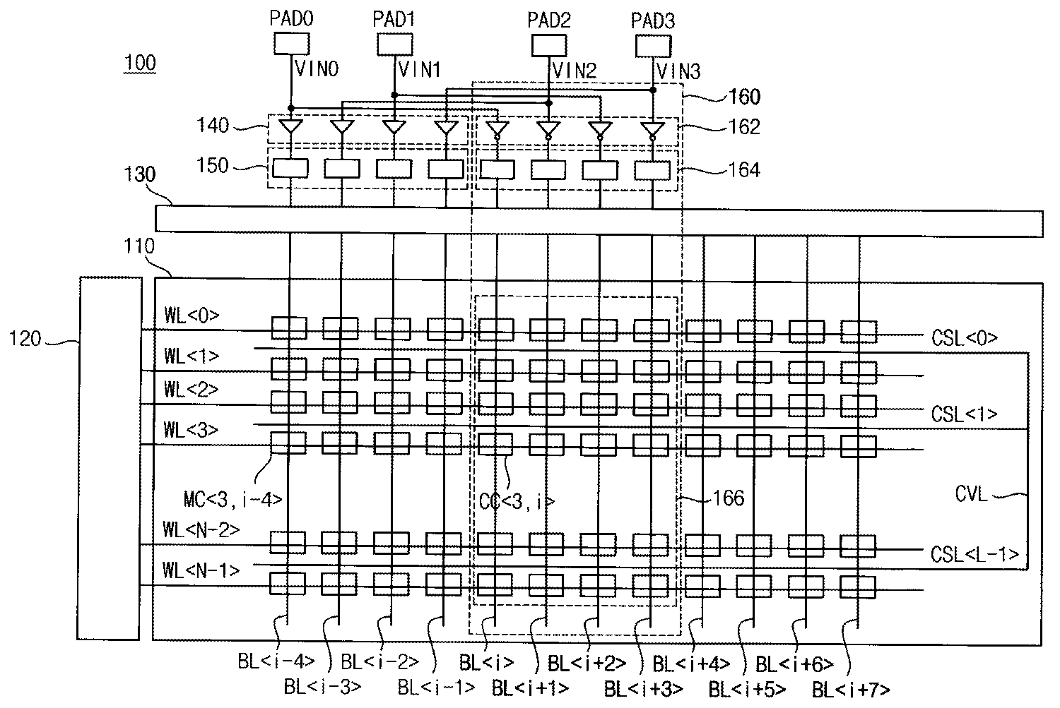
도 1은 본 발명에 의한 반도체 메모리 장치의 바람직한 일 실시예의 블록도를 나타낸다. 1 shows a block diagram of a preferred embodiment of a semiconductor memory device according to the present invention.
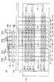
도 1을 참조하면, 반도체 메모리 장치(100)는 셀 어레이(110), 로우 디코더(120), 칼럼 디코더(130), 노말 입력버퍼(140), 노말 쓰기회로(150) 및 공통 소스 라인 보상회로(160)를 포함한다. 1, a
일실시예에서 반도체 메모리 장치(100)는 설명의 편의상 4비트 데이터를 입출력하는 구조로 도시되어 있으나 동일한 개념으로 X8, X16, X32 등으로 확장 가능하다. In one embodiment, the
공통 소스라인 보상회로(160)는 보상 입력버퍼(162), 보상 쓰기 회로(164), 복수의 보상 셀 유닛들(166)을 포함한다. The common source
셀 어레이(110)는 비트라인들(BL<i-4>~BL<i+7>)과 워드라인들(WL<0>~WL<N-1>)의 교차부위들에 각각 결합된 복수의 셀 유닛들을 포함한다. 두 개의 워드라인들(WL<0>, WL<1>),(WL<2>, WL<3>), ------, (WL<N-2>, WL<N-1>) 사이에 각각 공통소스라인들(CSL<0>, CSL<1>, ------, CSL<L-1>)이 배치되고 모든 공통소스라인들 (CSL<0>, CSL<1>, ------, CSL<L-1>)은 공통수직라인(CVL)에 의해 서로 전기적으로 결합된다. 이와 같은 공통 소스라인 구조는 셀당 6F2(= 2F ㅧ 3F)의 사이즈를 만족시킨다. The
워드라인 방향의 중앙에는 보상 셀 유닛들(166 : CC(<i,j>)이 배치되고, 그 좌우에는 노말 셀 유닛들(MC<i,j>)이 배치된다. 이와 같은 보상 셀 유닛들의 배치는 셀들의 공간배치에 따른 편차를 최소화하기 위한 것이다. 그러므로 최대 편차가 허용범위 이내라면 보상 셀 유닛들(166 : CC(<i,j>)의 공간 배치가 좌측 또는 우측 에지 부위에 배치될 수도 있다. 또한 보상 셀 유닛들(166 : CC(<i,j>)을 셀 어레이 공간 배에서 워드라인 방향으로 등간격으로 배치할 수도 있다. The compensation cell units 166: CC (<i, j>) are disposed at the center of the word line direction, and the normal cell units MC <i, j> Therefore, if the maximum deviation is within the permissible range, the spatial arrangement of the compensating cell units 166: CC (<i, j>) is placed at the left or right edge region It is also possible to arrange the compensation cell units 166: CC (<i, j>) equidistantly in the cell array space times in the word line direction.
그러므로 반도체 메모리 장치(100)의 셀 어레이(110)의 저장 공간은 N ㅧ (M + 4)로 구성할 수 있다. 여기서 실제 사용자가 사용 가능한 저장 공간은 노말 셀 유닛들로 구성되는 N ㅧ M 저장 공간으로 주어진다. Therefore, the storage space of the
본 발명의 보상 셀 유닛들(166)은 공통소스라인을 사용하는 저장 공간 단위, 예컨대 매트(MAT) 단위로 구성될 수 있다. The
공통 소스라인 보상회로(160)의 보상 입력버퍼(162)는 4개의 패드들(PAD0~PAD3)을 통해 입력되는 4비트 데이터의 각 비트들을 각각 버퍼링하기 위한 노말 입력버퍼(140)와 달리 반전된 상보 값을 버퍼링한다. The
도 2는 도 1의 셀 어레이의 셀 유닛의 등가 회로도를 나타내고, 도 3은 도 2의 셀 유닛의 가변저항 기억요소(ME)의 바람직한 일실시예의 사시도를 나타낸다. Fig. 2 shows an equivalent circuit diagram of the cell unit of the cell array of Fig. 1, and Fig. 3 shows a perspective view of a preferred embodiment of the variable resistance memory element ME of the cell unit of Fig.
도 2를 참조하면, 셀 유닛(MC)은 비트라인(BL)과 공통소스라인(CSL)에 직렬로 연결된 가변저항 기억요소(ME)와 셀 액세스 트랜지스터(MS)를 포함한다. 셀 액세스 트랜지스터(MS)는 게이트에 워드라인(WL)이 연결된 MOS 트랜지스터로 구성한다. Referring to Fig. 2, the cell unit MC includes a variable resistance memory element ME and a cell access transistor MS connected in series to the bit line BL and the common source line CSL. The cell access transistor MS is composed of a MOS transistor having a gate connected to the word line WL.
가변저항 기억소자(ME)는 도 3에 도시한 바와 같이 스핀전달토크(spin transfer torque)(STT)에 의해 데이터가 기록되는 STT-MTJ(Magnetic Tunnel Junction) 요소로 구성할 수 있다. STT-MTJ 요소(ME)는 고정층(FXL)과 자유층(FRL) 및 이들 사이에 터널층(TNL)을 포함할 수 있다. 고정층(FXL)의 자화 방향은, 예컨대, X축 방향으로 고정될 수 있다. 자유층(FRL)의 자화 방향은 조건에 따라 X축 방향 또는 그의 역방향이 될 수 있다. 고정층(FXL)에 접촉된 제1 전극(E1)이 구비될 수 있고, 자유층(FRL)에 접촉된 제2 전극(E2)이 구비될 수 있다. 여기서 제1 전극(E1)은 도 2의 비트라인(BL)과 연결되고, 제2 전극(E2)은 도 2의 공통소스라인(CSL)에 연결된다. The variable resistance memory element ME can be formed of a STT-MTJ (Magnetic Tunnel Junction) element in which data is written by a spin transfer torque (STT) as shown in FIG. The STT-MTJ element ME may include a fixed layer FXL and a free layer FRL and a tunnel layer TNL therebetween. The magnetization direction of the fixed layer FXL can be fixed, for example, in the X-axis direction. The magnetization direction of the free layer FRL may be in the X-axis direction or in the opposite direction depending on the conditions. The first electrode E1 may be provided in contact with the fixed layer FXL and the second electrode E2 may be provided in contact with the free layer FRL. Here, the first electrode E1 is connected to the bit line BL of FIG. 2, and the second electrode E2 is connected to the common source line CSL of FIG.
예컨대, 제1 전극(E1) 상에 고정층(FXL), 터널층(TNL), 자유층(FRL) 및 제2 전극(E2)이 순차로 구비될 수 있다. 도시하지는 않았지만, 제1 전극(E1)과 고정층(FXL) 사이에 고정층(FXL)의 자화 방향을 고정시켜 주기 위한 요소, 예컨대, 반강자성층(anti-ferromagnetic layer)이 더 구비될 수 있다. 제1 및 제2 전극(E1, E2)은 배선 형태를 가질 수 있고, 이 경우, 서로 평행 또는 수직하게 구비될 수 있다. 제1 및 제2 전극(E1, E2) 사이에 쓰기전류(WC1, WC2)를 인가할 수 있다. 상기 쓰기전류(WC1, WC2)의 방향에 따라, 자유층(FRL)의 자화 방향이 결정될 수 있다. 예컨대, 제2 전극(E2)에서 제1 전극(E1)으로 제1 쓰기전류(WC1)를 인가하면, 자유층(FRL)은 고정층(FXL)과 동일한 방향으로 자화될 수 있다. 보다 상세히 설명하면, 상기 제1 쓰기전류(WC1)에 의해 전자가 제1 전극(E1)에서 제2 전극(E2)으로 이동한다. 이때, 고정층(FXL)과 동일한 스핀 방향을 갖는 전자들이 자유층(FRL)에 토크(torque)를 인가할 수 있다. 이에 따라, 자유층(FRL)은 고정층(FXL)과 동일한 방향으로 자화될 수 있다. 제1 전극(E1)에서 제2 전극(E2)으로 제2 쓰기전류(WC2)를 인가하면, 자유층(FRL)은 고정층(FXL)과 반대 방향으로 자화될 수 있다. 이는 제2 쓰기전류(WC2)에 의해 전자가 제2 전극(E2)에서 제1 전극(E1)으로 흐르는데, 이때, 고정층(FXL)과 반대의 스핀을 갖는 전자들이 자유층(FRL)으로 되돌아와 토크를 인가하기 때문이다. 이와 같이, STT-MTJ 요소(ME)에서 자유층(FRL)의 자화 방향은 스핀전달토크(spin transfer torque)에 의해 변할 수 있다. 자유층(FRL)의 자화 방향이 고정층(FXL)의 자화 방향(우측방향)과 동일할 때, STT-MTJ 요소(ME)는 낮은 저항값을 갖고, 반대인 경우(좌측방향)에 높은 저항값을 갖는다. STT-MTJ 요소(ME)가 낮은 저항값을 가질 때, 데이터 '0'에 대응되고, 높은 저항값을 가질 때, 데이터 '1'에 대응된다고 할 수 있다. For example, the fixed layer FXL, the tunnel layer TNL, the free layer FRL, and the second electrode E2 may be sequentially formed on the first electrode E1. Although not shown, an element for fixing the magnetization direction of the fixed layer FXL may be further provided between the first electrode E1 and the fixed layer FXL, for example, an anti-ferromagnetic layer. The first and second electrodes E1 and E2 may have a wiring shape, and in this case, they may be provided parallel or perpendicular to each other. The write currents WC1 and WC2 can be applied between the first and second electrodes E1 and E2. The magnetization direction of the free layer FRL can be determined according to the direction of the write currents WCl and WC2. For example, when the first write current WC1 is applied from the second electrode E2 to the first electrode E1, the free layer FRL can be magnetized in the same direction as the fixed layer FXL. In more detail, electrons are moved from the first electrode E1 to the second electrode E2 by the first write current WC1. At this time, electrons having the same spin direction as that of the fixed layer FXL can apply torque to the free layer FRL. Accordingly, the free layer FRL can be magnetized in the same direction as the fixed layer FXL. When the second write current WC2 is applied from the first electrode E1 to the second electrode E2, the free layer FRL can be magnetized in the opposite direction to the fixed layer FXL. This causes electrons to flow from the second electrode E2 to the first electrode E1 by the second write current WC2. At this time, electrons having a spin opposite to the fixed layer FXL return to the free layer FRL This is because the torque is applied. Thus, the magnetization direction of the free layer FRL in the STT-MTJ element ME can be changed by the spin transfer torque. When the magnetization direction of the free layer FRL is equal to the magnetization direction (right direction) of the fixed layer FXL, the STT-MTJ element ME has a low resistance value, and in the opposite case (left direction) Respectively. When the STT-MTJ element ME has a low resistance value, it corresponds to data '0', and when it has a high resistance value, it corresponds to data '1'.
도 4는 도 1의 노말 입력버퍼(140)의 바람직한 일 실시예의 구체적인 회로 구성을 나타내고 도 5는 도 1의 보상 입력버퍼(162)의 바람직한 일 실시예의 구체적인 회로 구성을 나타낸다. FIG. 4 shows a specific circuit configuration of a preferred embodiment of the
노말 입력버퍼(140)는 4개의 의사 차동 증폭기들(Pseudo differential amplifier)(PDA0~PDA3)을 포함한다. 각 의사 차동 증폭기들(PDA0~PDA3) 각각은 패드들(PAD0~PAD3)로부터 입력된 데이터 비트신호들(VIN0~VIN3)를 일측 입력단자에 각각 입력하고 타측 입력단자에는 기준전압신호(VREF)를 공통으로 입력한다. 각 의사 차동 증폭기들(PDA0~PDA3)은 두 입력신호의 차이를 증폭하여 비반전 출력단자들 각각에 출력신호들(VOUT0~VOUT3)을 각각 출력한다. The
보상 입력버퍼(162)는 4개의 의사 차동 증폭기들(Pseudo differential amplifier)(PDA0B~PDA3B)을 포함한다. 각 의사 차동 증폭기들(PDA0B~PDA3B) 각각은 패드들(PAD0~PAD3)로부터 입력된 데이터 비트신호들(VIN0~VIN3)를 일측 입력단자에 각각 입력하고 타측 입력단자에는 기준전압신호(VREF)를 공통으로 입력한다. 각 의사 차동 증폭기들(PDA0B~PDA3B)은 두 입력신호의 차이를 증폭하여 반전 출력단자들 각각에 출력신호들(VOUT0B~VOUT3B)을 각각 출력한다. The
도 6은 도 1의 노말 쓰기회로의 바람직한 일 실시예의 구성을 나타내고, 도 7은 도 1의 보상 쓰기회로의 바람직한 일 실시예의 구성을 나타낸다. FIG. 6 shows a configuration of a preferred embodiment of the normal write circuit of FIG. 1, and FIG. 7 shows a configuration of a preferred embodiment of the compensation write circuit of FIG.
노말 쓰기 회로(150)의 4개의 노말 쓰기 드라이버들(NWD0, NWD1, NWD2, NWD3)은 각기 풀업 전류소스(PUCS), 풀업 트랜지스터(PUTR), 풀다운 전류소스(PDCS), 풀다운 트랜지스터(PDTR)를 포함한다. 그러므로 노말 입력버퍼(140)의 출력신호들(VOUT0, VOUT1, VOUT2, VOUT3)을 각각 입력한다. The four normal write drivers NWD0, NWD1, NWD2 and NWD3 of the
입력된 신호의 상태가 데이터 "0"이면 PMOS 트랜지스터로 구성된 풀업 트랜지스터(PUTR)가 턴온되어 풀업 전류소스(PUCS)로부터 공급된 쓰기전류를 컬럼 디코더(130)를 통해 선택된 비트라인으로 출력한다. The pull-up transistor PUTR constituted by the PMOS transistor is turned on to output the write current supplied from the pull-up current source PUCS to the selected bit line through the
입력된 신호의 상태가 데이터 "1"이면 NMOS 트랜지스터로 구성된 풀다운 트랜지스터(PDTR)가 턴온되어 컬럼디코더(130)를 통해 선택된 비트라인으로부터 공급된 전류를 풀다운 전류소스(PUCS)를 통해 그라운드로 싱크한다.The pull-down transistor PDTR constituted of the NMOS transistor is turned on to sink the current supplied from the selected bit line through the
그러므로 입력된 데이터의 상태에 응답하여 전류방향이 정반대인 쓰기전류로 컬럼 디코더(130)에 의해 선택된 비트라인을 드라이브 한다. Thus, in response to the state of the input data, the bit line selected by the
도 7을 참조하면 보상 쓰기회로(164)는 4개의 보상쓰기 드라이버들(CWD0, CWD1, CWD2, CWD3)을 포함한다. 4개의 보상 쓰기 드라이버들(CWD0, CWD1, CWD2, CWD3)은 노말 쓰기회로(150)의 4개의 노말 쓰기 드라이버들(NWD0, NWD1, NWD2, NWD3)과 동일한 회로 구성을 가진다.Referring to FIG. 7, the
보상 쓰기 회로(164)의 4개의 보상 쓰기 드라이버들(CWD0, CWD1, CWD2, CWD3)은 마찬가지로 각기 풀업 전류소스(PUCS), 풀업 트랜지스터(PUTR), 풀다운 전류소스(PDCS), 풀다운 트랜지스터(PDTR)를 포함한다. 그러므로 보상 입력버퍼(162)의 출력신호들(VOUT0B, VOUT1B, VOUT2B, VOUT3B)을 각각 입력한다. 4개의 보상 쓰기 드라이버들(CWD0, CWD1, CWD2, CWD3)의 출력은 컬럼 디코더(130)를 거치지 않고 비트라인들(BLi, BLi+1, BLi+2, BLi+3)에 각각 직접 연결된다. The four compensation write drivers CWD0, CWD1, CWD2 and CWD3 of the
따라서 보상 쓰기 회로(164)는 노말 쓰기 회로(150)에 입력된 신호와 상태가 반전된 신호가 입력되므로 4개의 보상 쓰기 드라이버들(CWD0, CWD1, CWD2, CWD3)에서 출력되는 4개의 전류신호는 4개의 노말 쓰기 드라이버들(NWD0, NWD1, NWD2, NWD3) 각각에서 출력되는 전류신호와는 상반되는 흐름방향을 가진다. Therefore, since the signal input to the
도 8은 본 발명에 의한 반도체 메모리 장치에서 데이터 패턴 "0001"에 따른 공통소스라인 보상동작을 설명하기 위한 회로도이다. 8 is a circuit diagram for explaining a common source line compensation operation according to a data pattern "0001" in the semiconductor memory device according to the present invention.
도 8에서는 로우 디코더(120)에 의해 워드라인(WL<0>)이 선택되고, 칼럼 디코더(130)에 의해 비트라인들((BL<i-4>, BL<i-3>, BL<i-2>, BL<i-1>)이 각각 선택된 것으로 가정하여 셀 유닛들(MC<0, i-4>, MC<0, i-3>, MC<0, i-2>, MC<0, i-1>)에 "0001" 데이터를 저장하는 것으로 가정한다. In FIG. 8, the word line WL <0> is selected by the
도 8을 참조하면, 데이터"0001"에 대응하여 노말 쓰기 드라이버들(NWD0~NWD3)의 각 입력측에는 노말 입력버퍼(140)의 출력신호들(VOUT0~VOUT3)의 상태인 "0001"이 인가된다. 그러므로 노말 쓰기 드라이버들(NWD0~NWD2)의 풀업 트랜지스터들(PUTR)이 턴온되어 풀업전류소스(PUCS)로부터 선택된 비트라인들(BL<i-4>, BL<i-3>, BL<i-2>)로 쓰기전류를 공급한다. 또한 노말 쓰기 드라이버들(NWD3)의 풀다운 트랜지스터들(PDTR)이 턴온되어 선택된 비트라인들(BL<i-1>)로부터 제공된 쓰기전류를 그라운드로 싱크한다. 그러므로 셀 유닛들(MC<0, i-4>, MC<0, i-3>, MC<0, i-2>)의 각 가변저항 기억요소들에는 도시된 화살표 방향(하측방향) 즉 비트라인으로부터 공통소스라인으로 쓰기전류가 흐르게 되므로 자유층의 자화장향이 고정층의 자화방향과 동일한 방향으로 자화된다. 그러므로 가변저항 기억요소의 저항값이 낮은 값으로 세팅되어 데이터 "0"을 저장한다. 한편 셀 유닛(MC<0, i-1>)의 가변저항 기억요소에는 도시된 화살표 방향(상측방향) 즉 공통소스라인으로부터 비트라인으로 쓰기전류가 흐르게 되므로 자유층의 자화장향이 고정층의 자화방향과 반대 방향으로 자화된다. 그러므로 가변저항 기억요소의 저항값이 높은 값으로 세팅되어 데이터 "1"을 저장한다.8, "0001" which is the state of the output signals VOUT0 to VOUT3 of the
여기서 공통소스라인(CSL<0>)을 전류 합류 노드로 보면 이 노드로 셀 유닛들(MC<0, i-4>, MC<0, i-3>, MC<0, i-2>)로부터 3개의 쓰기 전류들이 들어오는 방향인 반면에 이 노드로부터 셀 유닛(MC<0, i-1>)으로 하나의 전류가 나가는 방향이다. 그러므로 데이터 패턴에 따라 공통소스라인(CSL)에 들어오고 나가는 전류의 크기가 불균형을 이루게 된다. 이와 같은 전류 불균형은 공통소스라인의 전압레벨을 1/2VDD 상태에서 VDD 방향 또는 그라운드 방향으로 치우치게 작용할 수 있다. 이는 기억요소의 자화방향정도에 영향을 주게 되므로 쓰기 특성마진을 저하시킨다. (MC <0, i-4>, MC <0, i-3>, MC <0, i-2>) is connected to the common source line CSL <0> Is a direction in which three write currents flow from the node to the cell unit MC < 0, i-1 >. Therefore, the magnitude of the current flowing into and out of the common source line CSL becomes unbalanced according to the data pattern. Such a current imbalance can act to bias the voltage level of the common source line from the 1 / 2VDD state to the VDD direction or the ground direction. This affects the degree of magnetization of the memory element, thereby lowering the write characteristic margin.
본 발명에서는 데이터 "0001"에 대응하여 보상 입력회로(162)에서 "1110" 데이터를 생성하여 보상 쓰기회로(164)에 출력한다. 보상 쓰기회로(164)에서는 보상 입력회로(162)의 출력신호들(VOUT0B, VOUT1B, VOUT2B, VOUT3B)을 입력한다. 이들 신호에 응답하여 보상 쓰기 드라이버들(CWD0~CWD2)의 풀다운 트랜지스터들(PDTR)이 턴온되어 풀다운 전류소스(PDCS)로 보상 비트라인들(BL<i>, BL<i+1>, BL<i+2>)의 쓰기전류를 싱크한다. 또한 보상 쓰기 드라이버(CWD3)의 풀업 트랜지스터(PUTR)가 턴온되어 보상 비트라인(BL<i+3>)에 쓰기전류를 제공한다. 그러므로 보상 셀 유닛들(CC<0, i>, CC<0, i+1>, MC<0, i+2>)의 각 가변저항 기억요소들에는 도시된 화살표 방향(상측방향) 즉 공통소스라인으로부터 비트라인으로 쓰기전류가 흐르게 되므로 자유층의 자화장향이 고정층의 자화방향과 반대 방향으로 자화된다. 그러므로 가변저항 기억요소의 저항값이 높은 값으로 세팅되어 데이터 "1"을 저장한다. 한편 보상 셀 유닛(CC<0, i+3>)의 가변저항 기억요소에는 도시된 화살표 방향(하측방향) 즉 비트라인으로부터 공통소스라인으로 쓰기전류가 흐르게 되므로 자유층의 자화장향이 고정층의 자화방향과 동일한 방향으로 자화된다. 그러므로 가변저항 기억요소의 저항값이 낮은 값으로 세팅되어 데이터 "0"을 저장한다.In the present invention, the
그러므로 데이터 "0001"을 동시에 4개의 셀 유닛에 저장할 경우에 본 발명에서는 공통소스라인에서 보면 들어오는 전류의 수는 셀 유닛들(MC<0, i-4>, MC<0, i-3>, MC<0, i-2>)과 보상 셀 유닛(CC<0, i+3>)의 쓰기전류들로 총 4개가 된다. 한편, 공통소스라인에서 보면 나가는 전류의 수는 셀 유닛(MC<0, i-1>)과 보상 셀 유닛들(CC<0, i>, CC<0, i+1>, MC<0, i+2>)의 쓰기전류들로 총 4개가 된다. Therefore, when the data "0001" is stored in four cell units at the same time, in the present invention, the number of incoming currents in the common source line is equal to the number of cell units (MC < 0, i- MC <0, i-2>) and the compensation cell units (CC <0, i + 3>). On the other hand, the number of outgoing currents in the common source line is equal to the number of the cell units MC <0, i-1> and the compensation cell units CC <0, i>, CC <0, i + i + 2>) write currents.
따라서 공통소스라인에 들어오는 전류의 크기와 나가는 전류의 크기가 데이터 패턴에 관계없이 항상 동일 크기로 균형을 이루게 되므로 쓰기나 읽기 오류 발생을 방지할 수 있다.Therefore, the magnitude of the current flowing into the common source line and the magnitude of the outgoing current are always balanced at the same magnitude irrespective of the data pattern, so that a write or read error can be prevented.
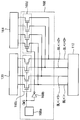
도 9는 본 발명에 의한 반도체 메모리 장치의 다른 실시예의 블록도를 나타낸다. 9 shows a block diagram of another embodiment of the semiconductor memory device according to the present invention.
도 9의 다른 실시예는 상술한 도 1의 일 실시예와 비교하면 공통 소스 라인 보상회로(160)에 보상모드 선택회로(168)가 더 추가된 점이 다르다. 그러므로 동일 부분에 대해서는 동일 부호로 처리하고 구체적인 설명은 생략한다. 9 differs from the above-described embodiment of FIG. 1 in that a compensation
다른 실시예에서는 셀 어레이(110)에 별도의 보상 셀 유닛들을 추가하지 않고 통상의 N ㅧ M 사이즈 내의 노말 셀 유닛들 중 일부를 보상 셀 유닛으로 사용하는 구조를 제시한다. 그러므로 보상 셀 유닛 수를 제외하면 사용자가 실제 사용 가능한 저장 공간은 N ㅧ (M - 4) 이다. 보상모드가 세트된 경우에 메모리 컨트롤러에서는 보상 셀 유닛으로 구성된 저장 공간을 제외한 N ㅧ (M - 4) 저장공간에 대해서만 어드레싱 제어하는 조건으로 한정된다. In another embodiment, a structure is shown in which some of the normal cell units within the normal N M size are used as a compensation cell unit without adding additional compensation cell units to the
그러므로 다른 실시예에서는 저장 공간이 다소 줄어들지만 주변 회로 영역에 간단한 회로를 추가하는 것에 의해 노이즈 삭제 기능을 추가시킬 수 있는 잇점이 있다. 또한 모드세트 레지스터를 사용하여 노이즈 삭제 기능을 선택적으로 세팅할 수 있다는 점에서 시스템 엔지니어가 노이즈 삭제 기능을 소프트웨어적으로 선택할 수 있다. Therefore, in other embodiments, the storage space is somewhat reduced, but there is an advantage in that the noise cancellation function can be added by adding a simple circuit to the peripheral circuit area. In addition, the system engineer can select the noise cancellation function in software in that the noise cancellation function can be selectively set using the mode set register.
도 10은 도 9의 보상모드 선택회로(168)의 구체적인 회로 구성을 나타낸다. FIG. 10 shows a specific circuit configuration of the compensation
도 10을 참조하면, 보상모드 선택회로(168)는 보상모드 세트 레지 스터(168a), 인버터(168b), 제1선택스위치(168c), 제2선택스위치(169d)를 포함한다.10, the compensation
보상모드 세트 레지스터(168a)는 외부로부터 보상모드 선택신호를 입력하여 보상모드 세트신호를 저장한다. 본 실시예에서는 레지스터에 저장된 데이터가"1"이면 노말 모드 세팅상태이고 "0"이면 보상모드 세팅상태라고 가정한다. 그러므로 보상모드 세트 레지스터(168a)는 저장된 데이터가 "1"이면 하이상태로 되고 "0"이면 로우상태로 되는 보상모드 선택신호(CMS)를 출력한다. The compensation mode set
제1선택스위치(168c)는 4개의 모스 트랜지스터들로 구성되고 칼럼 디코더(130)와 비트라인들(BL<i>, BL<i+1>, BL<i+2>, BL<i+3>)의 연결을 스위칭한다. 제1선택스위치(168c)는 4개의 모스 트랜지스터들은 보상모드 선택신호(CMS)의 하이상태에 응답하여 턴온된다. 즉 노말 모드에서는 제1선택스위치(168c)를 통해 칼럼 디코더(130)와 비트라인들(BL<i>, BL<i+1>, BL<i+2>, BL<i+3>)이 연결된다. 그러므로 노말 모드에서는 칼럼 디코더(130)를 통해 비트라인들(BL<i>, BL<i+1>, BL<i+2>, BL<i+3>)이 선택되면 노말 쓰기회로(140)에 의해 쓰기 전류가 공급된다. The
제2선택스위치(168d)는 4개의 모스 트랜지스터들로 구성되고 보상 쓰기회로(164)와 비트라인들(BL<i>, BL<i+1>, BL<i+2>, BL<i+3>)의 연결을 스위칭한다. 제2선택스위치(168d)는 4개의 모스 트랜지스터들은 인버터(168b)를 통해 인가되는 보상모드 선택신호(CMS)의 로우상태에 응답하여 턴온된다. 즉 보상모드에서는 제2선택스위치(168d)를 통해 보상 쓰기회로(164)와 비트라인들(BL<i>, BL<i+1>, BL<i+2>, BL<i+3>)이 연결된다. 그러므로 보상모드에서는 노말 쓰기회로(140)에 연동되어 비트라인들(BL<i>, BL<i+1>, BL<i+2>, BL<i+3>)에 보상 쓰기회로(164)에 의해 보상 쓰기 전류가 공급된다. The second
도 11은 도 1의 반도체 메모리 장치(100)를 포함하는 메모리 시스템(200)을 보여주는 블록도이다. FIG. 11 is a block diagram showing a
도 11을 참조하면, 메모리 시스템(200)은 반도체 메모리 장치(100) 및 메모리 컨트롤러(210)를 포함한다. Referring to FIG. 11, the
메모리 컨트롤러(210)는 호스트(Host) 및 반도체 메모리 장치(100)에 연결된다. 호스트(Host)의 요청에 응답하여, 컨트롤러(210)는 반도체 메모리 장치(100)를 액세스하도록 구성된다. 예를 들면, 메모리 컨트롤러(210)는 호스트(Host)의 요청에 응답하여 반도체 메모리 장치(100)의 읽기, 쓰기, 그리고 소거 동작을 제어하도록 구성된다. 메모리 컨트롤러(210)는 반도체 메모리 장치(100)의 동작을 제어하도록 구성된다. 메모리 컨트롤러(210)는 반도체 메모리 장치(100) 및 호스트(Host) 사이에 인터페이스를 제공하도록 구성된다. 메모리 컨트롤러(210)는 반도체 메모리 장치(100)를 제어하기 위한 펌웨어(firmware)를 구동하도록 구성된다.The
메모리 컨트롤러(210)는 반도체 메모리 장치(100)에 제어 신호(CTRL) 및 어드레스(ADDR)를 제공하도록 구성된다. 그리고 메모리 컨트롤러(210)는 반도체 메모리 장치(100)와 데이터(DATA)를 교환하도록 구성된다. 메모리 컨트롤러(210)는 램(RAM, Random Access Memory), 프로세싱 유닛(processing unit), 호스트 인터페이스(host interface), 그리고 메모리 인터페이스(memory interface)와 같은 잘 알려진 구성 요소들을 포함한다. 램(RAM)은 프로세싱 유닛의 동작 메모리, 반도체 메모리 장치(100) 및 호스트(Host) 사이의 캐시 메모리, 그리고 반도체 메모리 장치(100) 및 호스트(Host) 사이의 버퍼 메모리 중 적어도 하나로서 이용된다. 프로세싱 유닛은 메모리 컨트롤러(210)의 제반 동작을 제어한다.The
호스트 인터페이스는 호스트(Host) 및 컨트롤러(210) 사이의 데이터 교환을 수행하기 위한 프로토콜을 포함한다. 메모리 컨트롤러(210)는 USB (Universal Serial Bus) 프로토콜, MMC (multimedia card) 프로토콜, PCI (peripheral component interconnection) 프로토콜, PCI-E (PCI-express) 프로토콜, ATA (Advanced Technology Attachment) 프로토콜, Serial-ATA 프로토콜, Parallel-ATA 프로토콜, SCSI (small computer small interface) 프로토콜, ESDI (enhanced small disk interface) 프로토콜, 그리고 IDE (Integrated Drive Electronics) 프로토콜, Firewire 프로토콜, PCMCIA (Personal Computer Memory Card International Association) 프로토콜 등과 같은 다양한 인터페이스 프로토콜들 중 적어도 하나를 통해 외부(호스트)와 통신하도록 구성된다. 메모리 인터페이스는 반도체 메모리 장치(100)와 인터페이싱한다.The host interface includes a protocol for performing data exchange between the host (Host) and the
메모리 시스템(200)은 오류 정정 블록을 추가적으로 포함하도록 구성될 수 있다. 오류 정정 블록은 오류 정정 코드(ECC)를 이용하여 반도체 메모리 장치(100)로부터 읽어진 데이터의 오류를 검출하고, 정정하도록 구성된다. 오류 정정 블록은 메모리 컨트롤러(210)의 구성 요소로서 제공된다. 오류 정정 블록은 반도체 메모리 장치(100)의 구성 요소로서 제공될 수 있다.The
메모리 컨트롤러(210) 및 반도체 메모리 장치(100)는 하나의 반도체 칩으로 집적될 수 있다. 컨트롤러(210) 및 불휘발성 메모리 장치(100)는 하나의 반도체 칩으로 집적되어, 메모리 카드를 구성한다. 예를 들면, 컨트롤러(210) 및 반도체 메모리 장치(100)는 하나의 반도체 장치로 집적되어 PC 카드(PCMCIA, personal computer memory card international association), 스마트 미디어 카드(SM, SMC), 메모리 스틱, 멀티미디어 카드(MMC, RS-MMC, MMCmicro), SD 카드(SD, miniSD, microSD, SDHC) 등과 같은 메모리 카드를 구성한다.The
메모리 컨트롤러(210) 및 반도체 메모리 장치(100)는 하나의 반도체 장치로 집적되어 반도체 드라이브(SSD, Solid State Drive)를 구성한다. 반도체 드라이브(SSD)는 반도체 메모리에 데이터를 저장하도록 구성되는 저장 장치를 포함한다. 메모리 시스템(200)이 반도체 드라이브(SSD)로 이용되는 경우, 메모리 시스템(200)에 연결된 호스트(Host)의 동작 속도는 획기적으로 개선된다.The
다른 예로서, 메모리 시스템(200)은 컴퓨터, UMPC (Ultra Mobile PC), 워크스테이션, 넷북(net-book), PDA (Personal Digital Assistants), 포터블(portable) 컴퓨터, 타블렛 컴퓨터(tablet computer), 웹 타블렛(web tablet), 무선 전화기(wireless phone), 모바일 폰(mobile phone), 스마트폰(smart phone), e-북(e-book), PMP (portable multimedia player), 휴대용 게임기, 네비게이션(navigation) 장치, 블랙박스(black box), 디지털 카메라(digital camera), DMB (Digital Multimedia Broadcasting) 재생기, 디지털 음성 녹음기(digital audio recorder), 디지털 음성 재생기(digital audio player), 디지털 영상 녹화기(digital picture recorder), 디지털 영상 재생기(digital picture player), 디지털 동영상 녹화기(digital video recorder), 디지털 동영상 재생기(digital video player), 정보를 무선 환경에서 송수신할 수 있는 장치, 홈 네트워크를 구성하는 다양한 전자 장치들 중 하나, 컴퓨터 네트워크를 구성하는 다양한 전자 장치들 중 하나, 텔레매틱스 네트워크를 구성하는 다양한 전자 장치들 중 하나, RFID 장치, 또는 컴퓨팅 시스템을 구성하는 다양한 구성 요소들 중 하나 등과 같은 전자 장치의 다양한 구성 요소들 중 하나로 제공된다.As another example, the
반도체 메모리 장치(100) 또는 메모리 시스템(200)은 다양한 형태들의 패키지로 실장될 수 있다. 예를 들면, 반도체 메모리 장치(100) 또는 메모리 시스템(200)은 PoP(Package on Package), Ball grid arrays(BGAs), Chip scale packages(CSPs), Plastic Leaded Chip Carrier(PLCC), Plastic Dual In-Line Package(PDIP), Die in Waffle Pack, Die in Wafer Form, Chip On Board(COB), Ceramic Dual In-Line Package(CERDIP), Plastic Metric Quad Flat Pack(MQFP), Thin Quad Flatpack(TQFP), Small Outline(SOIC), Shrink Small Outline Package(SSOP), Thin Small Outline(TSOP), Thin Quad Flatpack(TQFP), System In Package(SIP), Multi Chip Package(MCP), Wafer-level Fabricated Package(WFP), Wafer-Level Processed Stack Package(WSP) 등과 같은 방식으로 패키지화되어 실장된다.The
도 12는 도 11에 도시된 메모리 시스템(200)을 포함하는 전자 장치의 일실시예를 나타낸다.12 illustrates one embodiment of an electronic device including the
도 12를 참조하면, 이동 전화기(cellular phone), 스마트 폰(smart phone), 또는 무선 인터넷 장치로서 구현될 수 있는 전자 장치(300)는 반도체 메모리 장치(100)와 반도체 메모리 장치(100)의 동작을 제어할 수 있는 메모리 컨트롤러(210)를 포함할 수 있다. 또한, 메모리 컨트롤러(210)는 전자 장치(300)의 전반적인 동작을 제어하는 호스트 프로세서(310)에 의하여 제어된다. 메모리 컨트롤러(210)는 반도체 메모리 장치(100)에 공통소스라인 노이즈 삭제방식에 의한 쓰기동작에 의해 동시에 X4, X8, X16 또는 X32 데이터들을 안전하게 저장할 수 있다. 반도체 메모리 장치(100)에 저장된 데이터는 호스트 프로세서(310)의 제어 하에 디스플레이(Display; 320)를 통하여 디스플레이 될 수 있다. 12, an
무선 송수신기(Radio Transceiver; 330)는 안테나(ANT)를 통하여 무선 신호들을 주거나 받을 수 있다. 예컨대, 무선 송수신기(330)는 안테나(ANT)를 통하여 수신된 무선 신호들을 호스트 프로세서(310)가 처리할 수 있는 신호들로 변환할 수 있다. 따라서 호스트 프로세서 (310)는 무선 송수신기(330)로부터 출력된 신호들을 처리하고, 처리된 신호들을 반도체 메모리(110)에 저장하거나 또는 디스플레이(320)를 통하여 디스플레이할 수 있다. 또한 무선 송수신기(330)는 호스트 프로세서(310)로부터 출력된 신호들을 무선 신호들로 변환하고, 변환된 무선 신호들을 안테나(ANT)를 통하여 외부로 출력할 수 있다.A
입력 장치(340)는 호스트 프로세서(310)의 동작을 제어하기 위한 제어 신호들 또는 프로세서(310)에 의하여 처리될 데이터를 입력할 수 있는 장치로서, 터치 패드 (touch pad)와 컴퓨터 마우스(computer mouse)와 같은 포인팅 장치(pointing device), 키패드(keypad), 또는 키보드로 구현될 수 있다.The
호스트 프로세서(310)는 반도체 메모리(110)로부터 출력된 데이터, 무선 송수신기 (330)로부터 출력된 무선 신호들, 또는 입력 장치(340)로부터 출력된 데이터가 디스플레이(320)를 통하여 디스플레이 될 수 있도록 디스플레이(320)의 동작을 제어할 수 있다.The
도 13은 도 11에 도시된 메모리 시스템(200)을 포함하는 전자 장치의 다른 실시예를 나타낸다.FIG. 13 shows another embodiment of an electronic device including the
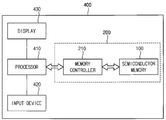
도 13을 참조하면, PC(personal computer), 테블릿 컴퓨터(tablet computer), 넷-북(net-book), e-리더(e-reader), PDA(personal digital assistant), PMP(portable multimedia player), MP3 플레이어, 또는 MP4 플레이어와 같은 데이터 처리 장치로 구현될 수 있는 전자 장치(400)는 반도체 메모리(100)와 반도체 메모리(100)의 동작을 제어할 수 있는 메모리 컨트롤러(210)를 포함한다.13, a personal computer (PC), a tablet computer, a net-book, an e-reader, a personal digital assistant (PDA) An
또한, 전자 장치(400)는 전자 장치(400)의 전반적인 동작을 제어하기 위한 호스트 프로세서(410)를 포함할 수 있다. 메모리 컨트롤러(210)는 전자 장치(400)의 전반적인 동작을 제어하는 호스트 프로세서(410)에 의하여 제어된다. 메모리 컨트롤러(210)는 반도체 메모리 장치(100)에 공통소스라인 노이즈 삭제방식에 의한 쓰기동작에 의해 동시에 X4, X8, X16 또는 X32 데이터들을 안전하게 저장할 수 있다. 호스트 프로세서(410)는 입력 장치(420)에 의하여 발생한 입력 신호에 따라 반도체 메모리(100)에 저장된 데이터를 디스플레이(430)를 통하여 디스플레이할 수 있다. 예컨대, 입력 장치(420)는 터치 패드 또는 컴퓨터 마우스와 같은 포인팅 장치, 키패드, 또는 키보드로 구현될 수 있다.In addition, the
도 14는 도 11에 도시된 메모리 시스템(200)을 포함하는 전자 장치의 또 다른 실시 예를 나타낸다.FIG. 14 shows another embodiment of an electronic device including the
도 14를 참조하면, 전자 장치(500)는 카드 인터페이스(Card Interface; 510), 메모리 컨트롤러(520), 도 1의 반도체 메모리 장치(100)를 포함한다.14, the
전자 장치(500)는 카드 인터페이스(510)를 통하여 호스트(HOST)와 데이터를 주거나 받을 수 있다. 실시 예에 따라 카드 인터페이스(510)는 SD(secure digital) 카드 인터페이스 또는 MMC(multi-media card) 인터페이스일 수 있으나 이에 한정되는 것은 아니다. 카드 인터페이스(510)는 전자 장치(500)와 통신할 수 있는 호스트(HOST)의 통신 프로토콜에 따라 호스트(HOST)와 메모리 컨트롤러(520) 사이에서 데이터 교환을 인터페이스 할 수 있다.The
메모리 컨트롤러(520)는 전자 장치(500)의 전반적인 동작을 제어하며, 카드 인터페이스(510)와 반도체 메모리 장치(100) 사이에서 데이터의 교환을 제어할 수 있다. 또한 메모리 컨트롤러(520)의 버퍼 메모리(522)는 카드 인터페이스(510)와 반도체 메모리 장치(100)사이에서 주고받는 데이터를 버퍼링할 수 있다. 메모리 컨트롤러(520)는 데이터 버스(DATA) 및 어드레스 버스(ADDRESS)를 통하여 카드 인터페이스(510)와 반도체 메모리 장치(100)와 연결된다. 실시예에 따라 메모리 컨트롤러(520)는 카드 인터페이스(510)로부터 읽기 또는 쓰고자 하는 데이터의 어드레스를 어드레스 버스를 통하여 수신하고 이를 반도체 메모리 장치(100)로 전달한다. The
또한, 메모리 컨트롤러(520)는 카드 인터페이스(510) 또는 반도체 메모리 장치(100) 각각에 연결된 데이터 버스를 통하여 읽기 또는 쓰고자 하는 데이터를 수신하거나 전송한다. 실시예에 따라 도 14에 도시된 메모리 컨트롤러(520)는 도 11에 도시된 메모리 컨트롤러(210)와 동일 또는 유사한 기능을 수행할 수 있다. 그러므로 메모리 컨트롤러(520)는 반도체 메모리 장치(100)에 공통소스라인 노이즈 삭제방식에 의한 쓰기동작에 의해 동시에 X4, X8, X16 또는 X32 데이터들을 안전하게 저장할 수 있다.In addition, the
도 14의 전자 장치(500)가 컴퓨터, 디지털 카메라, 디지털 오디오 플레이어, 이동 전화기, 콘솔 비디오 게임 하드웨어, 또는 디지털 셋-탑 박스와 같은 호스트 (HOST)에 접속될 때, 호스트(HOST)는 카드 인터페이스(510)와 메모리 컨트롤러 (520)를 통하여 반도체 메모리(100)에 저장된 데이터를 주거나 받을 수 있다.When the
도 15는 도 11에 도시된 메모리 시스템(200)을 포함하는 전자 장치의 또 다른 실시예를 나타낸다.Fig. 15 shows another embodiment of an electronic device including the
도 15를 참조하면, 전자 장치(600)는 카드 인터페이스(Card Interface; 610), 메모리 컨트롤러(620), 도 1의 반도체 메모리 장치(100)를 포함한다.Referring to FIG. 15, the
전자 장치(600)는 카드 인터페이스(610)를 통하여 호스트(HOST)와 데이터 통신을 수행할 수 있다. 실시 예에 따라 카드 인터페이스(610)는 SD(secure digital) 카드 인터페이스 또는 MMC(multi-media card) 인터페이스일 수 있으나 이에 한정되는 것은 아니다. 카드 인터페이스(610)는 전자 장치(600)와 통신할 수 있는 호스트(HOST)의 통신 프로토콜에 따라 호스트(HOST)와 메모리 컨트롤러(620) 사이에서 데이터 통신을 수행할 수 있다.The
메모리 컨트롤러(620)는 전자 장치(600)의 전반적인 동작을 제어하며, 카드 인터페이스(610)와 반도체 메모리 장치(100) 사이에서 데이터의 교환을 제어할 수 있다.The
또한, 메모리 컨트롤러(620)에 포함된 버퍼 메모리(622)는 전자 장치 (600)의 전반적인 동작을 제어하기 위하여 각종 데이터를 저장할 수 있다. 메모리 컨트롤러(620)는 데이터 버스(DATA) 및 로지컬 어드레스 버스(LOGICAL ADDRESS)를 통하여 카드 인터페이스(610)와 반도체 메모리 장치(100)와 접속될 수 있다. 실시 예에 따라 메모리 컨트롤러(620)는 카드 인터페이스(610)로부터 읽거나 또는 쓰고자 하는 데이터의 어드레스를 로지컬 어드레스 버스(LOGICAL ADDRESS)를 통하여 수신하고, 피지컬 어드레스 버스(PHYSICAL ADDRESS)를 통하여 반도체 메모리 장치(100)로 전달할 수 있다.The
또한, 메모리 컨트롤러(620)는 카드 인터페이스(610) 또는 반도체 메모리 장치(100) 각각에 접속된 데이터 버스(DATA)를 통하여 읽거나 또는 쓰고자 하는 데이터를 수신하거나 전송할 수 있다. 메모리 컨트롤러(620)는 도 11에 도시된 메모리 컨트롤러(210)와 동일 또는 유사한 기능을 수행할 수 있다. 따라서 메모리 컨트롤러(620)는 반도체 메모리 장치(100)에 공통소스라인 노이즈 삭제방식에 의한 쓰기동작에 의해 동시에 X4, X8, X16 또는 X32 데이터들을 안전하게 저장할 수 있다.The
도 15의 전자 장치(600)가 컴퓨터, 디지털 카메라, 디지털 오디오 플레이어, 이동 전화기, 콘솔 비디오 게임 하드웨어, 또는 디지털 셋-탑 박스와 같은 호스트(HOST)에 접속될 때, 호스트(HOST)는 카드 인터페이스(610)와 메모리 컨트롤러(620)를 통하여 반도체 메모리 장치(100)에 저장된 데이터를 주거나 받을 수 있다.When the
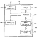
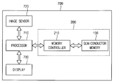
도 16은 도 11에 도시된 메모리 시스템(200)을 포함하는 전자 장치의 또 다른 실시예를 나타낸다.FIG. 16 shows another embodiment of an electronic device including the
도 16을 참조하면, 전자 장치(700)는 반도체 메모리 장치(100)와 반도체 메모리 장치(100)의 데이터 처리 동작을 제어하기 위한 메모리 컨트롤러(210), 및 전자 장치 (700)의 전반적인 동작을 제어할 수 있는 프로세서(710)를 포함한다. 메모리 컨트롤러(210)는 반도체 메모리 장치(100)에 공통소스라인 노이즈 삭제방식에 의한 쓰기동작에 의해 동시에 X4, X8, X16 또는 X32 데이터들을 안전하게 저장할 수 있다.16, the
전자 장치(700)의 이미지 센서(720)는 광학 이미지를 디지털 신호들로 변환하고, 변환된 디지털 신호들은 호스트 프로세서(710)의 제어 하에 반도체 메모리 장치(100)에 저장되거나 또는 디스플레이(730)를 통하여 디스플레이 된다. 또한, 반도체 메모리 장치(100)에 저장된 상기 디지털 신호들은 호스트 프로세서(710)의 제어 하에 디스플레이 (730)를 통하여 디스플레이 된다.The
본 발명은 단위 셀의 사이즈를 6F2구조로 하기 위한 공통소스 반도체 메모리 장치에서 공통소스노드에 유입되거나 유출되는 총 전류의 크기를 제로상태로 제어함으로써 데이터 패턴에 따른 공통소스라인 노이즈 발생을 방지할 수 있는 가변저항 기억소자를 가진 비휘발성 반도체 메모리 장치, 자기 메모리 장치(MRAM : Magnetic Random Access Memory) 중 STT-MRAM(Spin Torque Transfer-Magnetic Ramdom Access Memory)에 더욱 유용하게 이용될 수 있다.The present invention controls the size of the total current flowing into or out of the common source node in the common source semiconductor memory device to make the unit cell size 6F 2 structure zero state to prevent common source line noise generation according to the data pattern A nonvolatile semiconductor memory device having a variable resistance memory element and a STT-MRAM (Spin Torque Transfer-Magnetic Random Access Memory) in a magnetic random access memory (MRAM).
상술한 바와 같이, 본 발명의 바람직한 실시예를 참조하여 설명하였지만 해당 기술 분야에서 통상의 지식을 가진 자라면 하기의 특허청구범위에 기재된 본 발명의 사상 및 영역으로부터 벗어나지 않는 범위 내에서 본 발명을 다양하게 수정 및 변경시킬 수 있음을 이해할 수 있을 것이다.Although the preferred embodiments of the present invention have been disclosed for illustrative purposes, those skilled in the art will appreciate that various modifications, additions and substitutions are possible, without departing from the scope and spirit of the invention as disclosed in the accompanying claims. It will be understood that the invention may be modified and varied without departing from the scope of the invention.
Claims (10)
상기 복수의 노말 셀 유닛들을 통해 상기 공통소스라인에 동시 유입 및 유출되는 복수의 쓰기전류들을 상쇄시키기 위한 복수의 보상 쓰기전류들을 상기 공통소스라인에 공급하기 위한 공통소스라인 보상회로를 구비한 것을 특징으로 하는 반도체 메모리 장치.A cell array including a plurality of normal cell units each connected between a plurality of bit lines and a common source line; And
And a common source line compensation circuit for supplying a plurality of compensation write currents for canceling a plurality of write currents simultaneously flowing into and out of the common source line through the plurality of normal cell units to the common source line .
외부로부터 공급되는 쓰기 데이터를 반전 입력하기 위한 보상 입력버퍼;
상기 보상 입력버퍼를 통해 반전된 쓰기 데이터의 각 비트 값에 대응하는 보상 쓰기전류들을 대응하는 보상 비트라인들에 각각 동시에 공급하기 위한 보상 쓰기회로; 및
상기 셀 어레이의 영역에 배치되고 상기 보상 비트라인들과 상기 공통소스라인 사이에 각각 연결되고, 대응하는 보상 쓰기전류에 대응하는 데이터를 동시에 저장하기 위한 복수의 보상 셀 유닛들을 구비한 것을 특징으로 하는 반도체 메모리 장치. 2. The display device according to claim 1, wherein the common source line compensation circuit
A compensation input buffer for reversely inputting write data supplied from the outside;
A compensation write circuit for simultaneously supplying compensation write currents corresponding to respective bit values of write data inverted through said compensation input buffer to corresponding compensation bit lines; And
And a plurality of compensation cell units arranged in an area of the cell array and respectively connected between the compensation bit lines and the common source line, for simultaneously storing data corresponding to a corresponding compensation write current Semiconductor memory device.
상기 보상모드 선택회로는 보상모드세트신호에 응답하여 상기 보상 비트라인들을 선택하기 위한 칼럼 디코더를 통한 노말 쓰기전류와 상기 보상 쓰기회로를 보상 셀 유닛들에 선택적으로 공급하는 것을 특징으로 하는 반도체 메모리 장치.5. The semiconductor memory device according to claim 4, further comprising a compensation mode selection circuit between the compensation write circuit and the compensation bit lines,
Wherein the compensation mode selection circuit selectively supplies the compensation write circuit with a write write current and a normal write current through a column decoder for selecting the compensation bit lines in response to a compensation mode set signal. .
보상모드 세트신호를 저장하고 보상모드 선택신호를 발생하기 위한 보상모드 세트 레지스터;
상기 보상모드 선택신호를 반전시키기 위한 인버터;
상기 칼럼 디코더와 상기 보상 비트라인들 사이에 연결되고 상기 보상모드 선택신호에 응답하여 노말 모드에서 턴온 되는 제1선택스위치; 및
상기 보상 쓰기회로와 상기 보상 비트라인들 사이에 연결되고 상기 인버터의 출력신호에 응답하여 보상모드에서 턴온 되는 제2선택스위치를 구비한 것을 특징으로 하는 반도체 메모리 장치.6. The apparatus of claim 5, wherein the compensation mode selection circuit
A compensation mode set register for storing a compensation mode set signal and generating a compensation mode selection signal;
An inverter for inverting the compensation mode selection signal;
A first selection switch coupled between the column decoder and the compensation bit lines and being turned on in a normal mode in response to the compensation mode selection signal; And
And a second selection switch connected between the compensation write circuit and the compensation bit lines and being turned on in a compensation mode in response to an output signal of the inverter.
n(>1) 비트 데이터의 비트 수에 대응하는 비트라인들을 하나의 칼럼단위로 동시에 선택하기 위한 칼럼 디코더;
상기 복수의 워드라인들과 상기 복수의 비트라인들의 각 교차점에 배치되고, 대응하는 비트라인과 하나의 공통소스라인 사이에 각각 연결된 복수의 노말 셀 유닛들을 포함하는 셀 어레이;
상기 n 비트 데이터를 입력하기 위한 노말 입력버퍼;
상기 노말 입력버퍼에 입력된 데이터 패턴에 응답하여 상기 칼럼 디코더에 의해 선택된 칼럼의 비트라인들을 대응하는 쓰기전류로 각각 구동하기 위한 노말 쓰기회로: 및
상기 n 비트 데이터를 입력하여, 상기 노말 쓰기회로에 의해 동시 구동된 복수의 노말 셀 유닛들을 통해 상기 공통소스라인에 동시 유입 및 유출되는 복수의 쓰기전류들을 상쇄시키기 위한 복수의 보상 쓰기전류들을 상기 공통소스라인에 공급하기 위한 공통소스라인 보상회로를 구비한 것을 특징으로 하는 반도체 메모리 장치.A row decoder for selecting one of the plurality of word lines;
a column decoder for simultaneously selecting bit lines corresponding to the number of bits of n (> 1) bit data in units of one column;
A cell array disposed at each intersection of the plurality of word lines and the plurality of bit lines and including a plurality of normal cell units each connected between a corresponding bit line and a common source line;
A normal input buffer for inputting the n-bit data;
A normal write circuit for driving the bit lines of the column selected by the column decoder in response to a data pattern input to the normal input buffer with a corresponding write current, respectively;
A plurality of normal cell units connected in parallel to the common source line, and a plurality of normal cell units connected to the common source line, And a common source line compensation circuit for supplying the source line to the source line.
상기 n비트 데이터를 반전 입력하기 위한 보상 입력버퍼;
상기 보상 입력버퍼를 통해 반전된 데이터의 각 비트 값에 대응하는 보상 쓰기전류들을 대응하는 보상 비트라인들에 각각 동시에 공급하기 위한 보상 쓰기회로; 및
상기 셀 어레이의 영역에 배치되고 상기 보상 비트라인들과 상기 공통소스라인 사이에 각각 연결되고, 대응하는 보상 쓰기전류에 대응하는 데이터를 동시에 저장하기 위한 복수의 보상 셀 유닛들을 구비한 것을 특징으로 하는 반도체 메모리 장치. 8. The display device according to claim 7, wherein the common source line compensation circuit
A compensation input buffer for reversely inputting the n-bit data;
A compensation write circuit for simultaneously supplying compensation write currents corresponding to respective bit values of data inverted through said compensation input buffer to corresponding compensation bit lines; And
And a plurality of compensation cell units arranged in an area of the cell array and respectively connected between the compensation bit lines and the common source line, for simultaneously storing data corresponding to a corresponding compensation write current Semiconductor memory device.
상기 보상모드 선택회로는 보상모드 세트신호에 응답하여 상기 보상 비트라인들을 선택하기 위한 칼럼 디코더를 통한 노말 쓰기전류와 상기 보상 쓰기회로를 보상 셀 유닛들에 선택적으로 공급하는 것을 특징으로 하는 반도체 메모리 장치.9. The semiconductor memory device according to claim 8, further comprising a compensation mode selection circuit between the compensation write circuit and the compensation bit lines,
Wherein the compensation mode selection circuit selectively supplies the compensation write circuit with a write write current and a normal write current through a column decoder for selecting the compensation bit lines in response to a compensation mode set signal. .
보상모드 세트신호를 저장하고 보상모드 선택신호를 발생하기 위한 보상모드 세트 레지스터;
상기 보상모드 선택신호를 반전시키기 위한 인버터;
상기 칼럼 디코더와 상기 보상 비트라인들 사이에 연결되고 상기 보상모드 선택신호에 응답하여 노말 모드에서 턴온 되는 제1선택스위치; 및상기 보상 쓰기회로와 상기 보상 비트라인들 사이에 연결되고 상기 인버터의 출력신호에 응답하여 보상모드에서 턴온 되는 제2선택스위치를 구비한 것을 특징으로 하는 반도체 메모리 장치.10. The image pickup apparatus according to claim 9, wherein the compensation mode selection circuit
A compensation mode set register for storing a compensation mode set signal and generating a compensation mode selection signal;
An inverter for inverting the compensation mode selection signal;
A first selection switch coupled between the column decoder and the compensation bit lines and being turned on in a normal mode in response to the compensation mode selection signal; And a second selection switch connected between said compensation write circuit and said compensation bit lines and being turned on in a compensation mode in response to an output signal of said inverter.
Priority Applications (2)
| Application Number | Priority Date | Filing Date | Title |
|---|---|---|---|
| KR1020120145974A KR101996265B1 (en) | 2012-12-14 | 2012-12-14 | Common Soure Semiconductor Memory Apparatus |
| US14/105,782 US9076539B2 (en) | 2012-12-14 | 2013-12-13 | Common source semiconductor memory device |
Applications Claiming Priority (1)
| Application Number | Priority Date | Filing Date | Title |
|---|---|---|---|
| KR1020120145974A KR101996265B1 (en) | 2012-12-14 | 2012-12-14 | Common Soure Semiconductor Memory Apparatus |
Publications (2)
| Publication Number | Publication Date |
|---|---|
| KR20140077325A true KR20140077325A (en) | 2014-06-24 |
| KR101996265B1 KR101996265B1 (en) | 2019-07-04 |
Family
ID=50930713
Family Applications (1)
| Application Number | Title | Priority Date | Filing Date |
|---|---|---|---|
| KR1020120145974A Active KR101996265B1 (en) | 2012-12-14 | 2012-12-14 | Common Soure Semiconductor Memory Apparatus |
Country Status (2)
| Country | Link |
|---|---|
| US (1) | US9076539B2 (en) |
| KR (1) | KR101996265B1 (en) |
Families Citing this family (4)
| Publication number | Priority date | Publication date | Assignee | Title |
|---|---|---|---|---|
| TWI608476B (en) * | 2015-04-10 | 2017-12-11 | 格羅方德半導體私人有限公司 | Stt-mram bitcell for embedded flash applications |
| EP3506359A1 (en) | 2017-12-29 | 2019-07-03 | IMEC vzw | Memory device with magnetic tunnel junctions and method for manufacturing thereof |
| CN110136760B (en) * | 2018-02-09 | 2021-03-23 | 上海磁宇信息科技有限公司 | MRAM chip |
| US11031059B2 (en) * | 2019-02-21 | 2021-06-08 | Sandisk Technologies Llc | Magnetic random-access memory with selector voltage compensation |
Citations (2)
| Publication number | Priority date | Publication date | Assignee | Title |
|---|---|---|---|---|
| US20040008557A1 (en) * | 2002-07-12 | 2004-01-15 | Perner Frederick A. | Magnetic memory having a temperature compensated write circuit |
| KR100725373B1 (en) * | 2006-01-20 | 2007-06-07 | 삼성전자주식회사 | Flash memory device |
Family Cites Families (7)
| Publication number | Priority date | Publication date | Assignee | Title |
|---|---|---|---|---|
| KR100866731B1 (en) | 2002-09-04 | 2008-11-03 | 주식회사 하이닉스반도체 | Magnetoresistive ram |
| US7411815B2 (en) | 2005-11-14 | 2008-08-12 | Infineon Technologies Ag | Memory write circuit |
| US7742329B2 (en) | 2007-03-06 | 2010-06-22 | Qualcomm Incorporated | Word line transistor strength control for read and write in spin transfer torque magnetoresistive random access memory |
| KR101004506B1 (en) | 2008-09-09 | 2010-12-31 | 주식회사 하이닉스반도체 | Vertical magnetic nonvolatile memory device having a common source line and manufacturing method thereof |
| US7855923B2 (en) | 2008-10-31 | 2010-12-21 | Seagate Technology Llc | Write current compensation using word line boosting circuitry |
| KR101669550B1 (en) | 2009-09-10 | 2016-10-26 | 삼성전자주식회사 | Flash memory device reducing noise of common source line, operating method thereof, and memory system including that |
| KR101644979B1 (en) | 2010-02-01 | 2016-08-03 | 삼성전자주식회사 | Nonvolatile memory device and read method thereof |
-
2012
- 2012-12-14 KR KR1020120145974A patent/KR101996265B1/en active Active
-
2013
- 2013-12-13 US US14/105,782 patent/US9076539B2/en active Active
Patent Citations (2)
| Publication number | Priority date | Publication date | Assignee | Title |
|---|---|---|---|---|
| US20040008557A1 (en) * | 2002-07-12 | 2004-01-15 | Perner Frederick A. | Magnetic memory having a temperature compensated write circuit |
| KR100725373B1 (en) * | 2006-01-20 | 2007-06-07 | 삼성전자주식회사 | Flash memory device |
Also Published As
| Publication number | Publication date |
|---|---|
| KR101996265B1 (en) | 2019-07-04 |
| US20140169086A1 (en) | 2014-06-19 |
| US9076539B2 (en) | 2015-07-07 |
Similar Documents
| Publication | Publication Date | Title |
|---|---|---|
| US11438016B2 (en) | Error detection code generation circuits of semiconductor devices, memory controllers including the same and semiconductor memory devices including the same | |
| US9953702B2 (en) | Semiconductor memory devices, memory systems including the same and methods of operating the same | |
| US9773544B2 (en) | Memory device with switchable sense amplifier | |
| US10127102B2 (en) | Semiconductor memory devices and memory systems including the same | |
| KR101750457B1 (en) | Memory device using error correcting code and system there-of | |
| US10108370B2 (en) | Methods of reading nonvolatile memory devices | |
| JP5754710B2 (en) | Resistive memory device | |
| US20190139594A1 (en) | Semiconductor memory device and data path configuration method thereof | |
| KR20170108307A (en) | Non-volatile memory device and method of operating the same | |
| US9892773B2 (en) | Unit array of a memory device, memory device, and memory system including the same | |
| KR20120010664A (en) | Static Random Access Memory Device with Negative Voltage Level Shifter | |
| CN103928050A (en) | Memory Cell And Memory Device Having The Same | |
| KR20160035737A (en) | Solid state drive and computing system including the same | |
| US9293177B2 (en) | Semiconductor memory device, memory system including the same and operating method thereof | |
| JP2012094239A (en) | Semiconductor memory device and semiconductor memory system | |
| KR101996265B1 (en) | Common Soure Semiconductor Memory Apparatus | |
| CN107564564A (en) | Memory cell, memory device and its electronic equipment | |
| US9742355B2 (en) | Buffer circuit robust to variation of reference voltage signal | |
| US9378797B2 (en) | Provide a memory device capable of increasing performance by performing a write operation using stable multi voltages that are applied to a word line | |
| KR20160019595A (en) | Memory device including reference voltage generator | |
| US9324384B2 (en) | Sense amplifiers and memory devices having the same | |
| US20160154733A1 (en) | Method of operating solid state drive | |
| JP4932273B2 (en) | Arithmetic processing circuit using ferroelectric capacitor and arithmetic method | |
| CN112216325A (en) | Memory device including switching circuit operating independently of power supply voltage |
Legal Events
| Date | Code | Title | Description |
|---|---|---|---|
| PA0109 | Patent application |
Patent event code: PA01091R01D Comment text: Patent Application Patent event date: 20121214 |
|
| PG1501 | Laying open of application | ||
| A201 | Request for examination | ||
| PA0201 | Request for examination |
Patent event code: PA02012R01D Patent event date: 20171117 Comment text: Request for Examination of Application Patent event code: PA02011R01I Patent event date: 20121214 Comment text: Patent Application |
|
| E902 | Notification of reason for refusal | ||
| PE0902 | Notice of grounds for rejection |
Comment text: Notification of reason for refusal Patent event date: 20181031 Patent event code: PE09021S01D |
|
| E701 | Decision to grant or registration of patent right | ||
| PE0701 | Decision of registration |
Patent event code: PE07011S01D Comment text: Decision to Grant Registration Patent event date: 20190418 |
|
| GRNT | Written decision to grant | ||
| PR0701 | Registration of establishment |
Comment text: Registration of Establishment Patent event date: 20190628 Patent event code: PR07011E01D |
|
| PR1002 | Payment of registration fee |
Payment date: 20190701 End annual number: 3 Start annual number: 1 |
|
| PG1601 | Publication of registration | ||
| FPAY | Annual fee payment |
Payment date: 20220525 Year of fee payment: 4 |
|
| PR1001 | Payment of annual fee |
Payment date: 20220525 Start annual number: 4 End annual number: 4 |
|
| PR1001 | Payment of annual fee |
Payment date: 20240527 Start annual number: 6 End annual number: 6 |
|
| PR1001 | Payment of annual fee |
Payment date: 20250522 Start annual number: 7 End annual number: 7 |