KR20140077464A - Tspc dynamic flip flop having leakage current compensation function - Google Patents
Tspc dynamic flip flop having leakage current compensation function Download PDFInfo
- Publication number
- KR20140077464A KR20140077464A KR1020120146304A KR20120146304A KR20140077464A KR 20140077464 A KR20140077464 A KR 20140077464A KR 1020120146304 A KR1020120146304 A KR 1020120146304A KR 20120146304 A KR20120146304 A KR 20120146304A KR 20140077464 A KR20140077464 A KR 20140077464A
- Authority
- KR
- South Korea
- Prior art keywords
- node
- terminal
- logic value
- logic
- signal
- Prior art date
- Legal status (The legal status is an assumption and is not a legal conclusion. Google has not performed a legal analysis and makes no representation as to the accuracy of the status listed.)
- Ceased
Links
- 238000000034 method Methods 0.000 claims abstract description 9
- 238000010586 diagram Methods 0.000 description 9
- 239000003990 capacitor Substances 0.000 description 6
- 230000007257 malfunction Effects 0.000 description 6
- 230000003071 parasitic effect Effects 0.000 description 6
- 238000004088 simulation Methods 0.000 description 3
- 238000010835 comparative analysis Methods 0.000 description 1
- 230000007423 decrease Effects 0.000 description 1
- 230000000694 effects Effects 0.000 description 1
Images

Classifications
-
- H—ELECTRICITY
- H03—ELECTRONIC CIRCUITRY
- H03K—PULSE TECHNIQUE
- H03K3/00—Circuits for generating electric pulses; Monostable, bistable or multistable circuits
- H03K3/01—Details
- H03K3/012—Modifications of generator to improve response time or to decrease power consumption
-
- H—ELECTRICITY
- H03—ELECTRONIC CIRCUITRY
- H03K—PULSE TECHNIQUE
- H03K3/00—Circuits for generating electric pulses; Monostable, bistable or multistable circuits
- H03K3/02—Generators characterised by the type of circuit or by the means used for producing pulses
- H03K3/027—Generators characterised by the type of circuit or by the means used for producing pulses by the use of logic circuits, with internal or external positive feedback
- H03K3/037—Bistable circuits
-
- H—ELECTRICITY
- H03—ELECTRONIC CIRCUITRY
- H03K—PULSE TECHNIQUE
- H03K3/00—Circuits for generating electric pulses; Monostable, bistable or multistable circuits
- H03K3/02—Generators characterised by the type of circuit or by the means used for producing pulses
- H03K3/353—Generators characterised by the type of circuit or by the means used for producing pulses by the use, as active elements, of field-effect transistors with internal or external positive feedback
- H03K3/356—Bistable circuits
- H03K3/356104—Bistable circuits using complementary field-effect transistors
- H03K3/356165—Bistable circuits using complementary field-effect transistors using additional transistors in the feedback circuit
Landscapes
- Logic Circuits (AREA)
Abstract
본 발명은, 티에스피씨 동적 플립플롭에 피드백 회로 구조의 누설전류 보상회로를 추가하여 미세공정에서 제작된 CMOS 트랜지스터를 포함하는 티에스피씨 동적 플립플롭이 저속 동작부터 고속 동작까지 가능하도록 하는 기술에 관한 것이다.
이러한 본 발명은, 입력데이터와 클럭신호에 따른 로직값을 A 노드에 출력하는 제1로직부; 상기 클럭신호와 상기 A 노드로부터 공급되는 신호에 따른 로직값을 B 노드에 출력하는 제2로직부; 상기 B 노드로부터 공급되는 신호와 상기 클럭신호에 따른 로직값을 C 노드에 출력하는 제3로직부; 상기 C 노드로부터 공급되는 로직 값에 따라 Q 노드에 해당 데이터를 출력하는 출력부; 및 상기 제1-3 로직부의 A 내지 C 노드 중 임의의 노드가 플로팅 상태에 있을 때, 해당 노드의 논리값과 반대 논리값을 갖는 후단 노드의 신호를 해당 노드로 피드백시켜 해당 노드의 누설전류를 보상하는 누설전류 보상부;를 포함한다.The present invention relates to a technique for enabling a TS PC dynamic flip-flop including a CMOS transistor fabricated in a microprocessing process to be performed from a low-speed operation to a high-speed operation by adding a leakage current compensation circuit of a feedback circuit structure to a TS PC dynamic flip- .
According to another aspect of the present invention, there is provided a logic circuit comprising: a first logic unit for outputting logic values according to input data and a clock signal to an A node; A second logic unit for outputting a logic value according to the clock signal and the signal supplied from the node A to the node B; A third logic unit for outputting a signal supplied from the B node and a logic value according to the clock signal to the C node; An output unit for outputting the corresponding data to the Q node according to a logic value supplied from the C node; And when any one of the nodes A to C of the first to third logic units is in a floating state, a signal of a downstream node having a logic value opposite to that of the corresponding node is fed back to the corresponding node, And a compensating leakage current compensating unit.
Description
본 발명은 티에스피씨 동적 플립플롭(TSPC Dynamic Flip/Flop)의 설계 기술에 관한 것으로, 특히 미세공정에서 제작된 시모스(CMOS) 트랜지스터를 포함하는 동적 플립플롭에서 누설전류 증가에 의해 오동작이 발생되는 것을 방지할 수 있도록 한 누설전류 보상기능을 구비한 티에스피씨 동적 플립플롭에 관한 것이다.
BACKGROUND OF THE
도 1은 종래 기술에 의한 TSPC(True single pulse clocked) 동적 플립플롭(Dynamic Flip/Flop)의 회로도로서 이에 도시한 바와 같이, 제1-3로직부(11-13) 및 출력부(14)를 구비한다. FIG. 1 is a circuit diagram of a TSPC (True Single Pulse Clocked) dynamic flip-flop circuit according to the related art. As shown in FIG. 1, the 1-3 logic unit 11-13 and the
제1 로직부(11)는 전원단자(VDD)와 접지단자의 사이에 직렬접속된 제1,2 피모스 트랜지스터(PM1),(PM2) 및 제1 엔모스 트랜지스터(NM1)를 구비하여, 데이터(D)와 클럭신호(clk)에 따른 로직값을 A 노드에 출력한다. The
제1 피모스 트랜지스터(PM1) 및 제1 엔모스 트랜지스터(NM1)의 게이트에 공급되는 데이터(D)가 "1"일 때, A 노드의 로직값은 "0"이 된다. 제2 피모스 트랜지스터(PM2)의 게이트에 공급되는 클럭신호(clk)의 로직값이 "0"일 때 상기 A 노드의 로직값은 상기 데이터(D)의 반전된 값이 된다. 클럭신호(clk)의 로직값이 "1"이고, 상기 데이터(D)의 로직값이 "0"일 때 상기 A 노드는 플로팅(floating)되어 이전의 로직값을 유지(저장)한다.When the data D supplied to the gates of the first PMOS transistor PM1 and the first NMOS transistor NM1 is "1 ", the logic value of the A node becomes" 0 ". The logic value of the node A becomes the inverted value of the data D when the logic value of the clock signal clk supplied to the gate of the second PMOS transistor PM2 is "0 ". When the logic value of the clock signal clk is "1 ", and the logic value of the data D is" 0 ", the A node is floated to hold (store) the previous logic value.
제2 로직부(12)는 전원단자(VDD)와 접지단자의 사이에 직렬접속된 제3 피모스 트랜지스터(PM3) 및 제2,3 엔모스 트랜지스터(NM2),(NM3)를 구비하여, 상기 A 노드로부터 공급되는 로직값과 상기 클럭신호(clk)에 따른 로직값을 B 노드에 출력한다. The
제3 피모스 트랜지스터(PM3) 및 제3 엔모스 트랜지스터(NM3)의 게이트에 공급되는 클럭신호(clk)의 로직값이 "0"일 때 B 노드의 로직값은 "1"이다. 상기 클럭신호(clk)의 로직값이 "1"이고, 상기 A 노드로부터 제2 엔모스 트랜지스터(NM2)의 게이트에 공급되는 로직값이 "1"일 때 상기 B 노드의 로직값은 "0"이다. 상기 A 노드의 로직값이 "0"일 때 상기 B 노드는 플로팅(floating)되어 이전의 로직값을 유지한다.The logic value of the B node is "1" when the logic value of the clock signal clk supplied to the gates of the third PMOS transistor PM3 and the third NMOS transistor NM3 is "0 ". The logic value of the B node is "0" when the logic value of the clock signal clk is "1 ", and the logic value supplied from the A node to the gate of the second NMOS transistor NM2 is & to be. When the logic value of the A node is "0 ", the B node is floated and retains the previous logic value.
제3 로직부(13)는 전원단자(VDD)와 접지단자의 사이에 직렬접속된 제4 피모스 트랜지스터(PM4) 및 제4,5 엔모스 트랜지스터(NM4),(NM5)를 구비하여, 상기 B 노드로부터 공급되는 데이터와 상기 클럭신호(clk)에 따른 로직값을 C 노드에 출력한다. The
제4 피모스 트랜지스터(PM4) 및 제5 엔모스 트랜지스터(NM5)의 게이트에 공급되는 상기 B 노드의 로직값이 "0"일 때 상기 C 노드의 로직값은 "1"이다. 제4 엔모스 트랜지스터(NM4)의 게이트에 공급되는 상기 클럭신호(clk)의 로직값이 "1"일 때 상기 C 노드의 로직값은 상기 B 노드의 로직값의 반전된 로직값이 된다. 상기 클럭신호(clk)의 로직값이 "0"이고, 상기 B 노드의 로직값이 "1"일 때 상기 C 노드는 플로팅되어 이전의 로직값을 유지한다.The logic value of the C node is "1" when the logic value of the B node supplied to the gates of the fourth PMOS transistor PM4 and the fifth NMOS transistor NM5 is "0 ". The logic value of the C node becomes the inverted logic value of the logic value of the B node when the logic value of the clock signal clk supplied to the gate of the fourth NMOS transistor NM4 is "1 ". When the logic value of the clock signal clk is "0" and the logic value of the B-node is "1 ", the C-node floats to maintain the previous logic value.
출력부(14)는 전원단자(VDD)와 접지단자의 사이에 직렬접속된 제5 피모스 트랜지스터(PM5) 및 제6 엔모스 트랜지스터(NM6)를 구비하여, 상기 C 노드로부터 공급되는 로직 값에 따라 출력단자인 Q 노드에 해당 데이터를 출력한다.The
상기 C 노드로부터 제5 피모스 트랜지스터(PM5) 및 제6 엔모스 트랜지스터(NM6)의 게이트에 공급되는 로직값의 반전된 로직값이 Q 노드에 출력된다.The inverted logic value of the logic value supplied from the C node to the gates of the fifth PMOS transistor PM5 and the sixth NMOS transistor NM6 is outputted to the Q node.
결국, 상기 설명에서와 같이 상기 A 내지 C 노드는 플로팅 상태(구간)에 놓여 있을 때 이전의 로직값을 저장하고, 이렇게 저장된 로직값이 상기 Q 노드 측으로 순차적으로 전달되어 클럭신호(clk)의 한 주기 동안 저장된다. As a result, as described above, the A to C nodes store the previous logic value when they are in the floating state (interval), and the stored logic values are sequentially transmitted to the Q node side, and one of the clock signals clk Lt; / RTI >
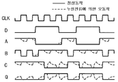
도 2는 상기 도 1에서 상기 A,B,C 노드, Q 노드, 데이터(D) 및 클럭신호(clk)의 타이밍도를 나타낸 것이다. 도 2에서 실선은 도 1의 TSPC 동적 플립플롭(10)이 정상동작 할 때의 파형도를 나타낸 것이고, 점선은 플로팅 시간이 길어져 누설전류에 의한 오동작 파형을 나타낸 것이다. FIG. 2 is a timing chart of the nodes A, B, and C, the node Q, the data D, and the clock signal clk in FIG. In FIG. 2, a solid line indicates a waveform when the TSPC dynamic flip-flop 10 shown in FIG. 1 operates normally, and a dotted line indicates a malfunction waveform due to a leakage current due to a long floating time.
상기 설명에서와 같이 상기 A 노드의 플로팅 구간은 클럭신호(clk)의 로직값이 "1"이고, 상기 데이터(D)의 로직값이 "0"일 때이며, B 노드의 로직값과 반전된 값을 가진다. 상기 B 노드의 플로팅 구간은 클럭신호(clk)의 로직값이 "1"이고, 상기 A 노드의 로직값이 "0"일 때이며, C 노드의 로직값과 반전된 값을 가진다. 상기 C 노드의 플로팅 구간은 클럭신호(clk)의 로직값이 "0"이고, 상기 B 노드의 로직값이 "1"일 때이며, Q 노드의 로직값과 반전된 값을 가진다. As described above, the floating period of the node A is when the logic value of the clock signal clk is "1 ", the logic value of the data D is" 0 ", and the logic value of the node B and the inverted value . The floating period of the B-node is when the logic value of the clock signal clk is "1", the logic value of the A-node is "0", and the logic value of the C-node is inverted. The floating period of the C node is when the logic value of the clock signal clk is "0 ", the logic value of the B node is" 1 ", and the logic value of the Q node is inverted.
결국, 상기 A,B,C 노드의 각 플로팅 구간은 클럭신호(clk)와 바로 이전 단 노드의 로직값에 의해 결정되고, 상기 결정된 로직값은 다음 단의 노드값과 반전된 값을 가진다. As a result, each floating interval of the nodes A, B, and C is determined by the clock signal clk and the logic value of the immediately preceding node, and the determined logic value has a value inverted from the next node value.
고속 동작을 요구하는 디지털 시스템에서 상기와 같은 TSPC 동적 플립플롭(10)이 이용된다. 이와 같은 TSPC 동적 플립플롭(10)은 상기 설명에서와 같이 플로팅 노드의 기생 커패시터에 충방전되는 전하에 의해 동작한다. 상기 플로팅 노드란 상기 피모스 트랜지스터(PM2,PM3, PM4)와 같은 CMOS 트랜지스터를 각기 통해 전원단자(VDD)와 연결되는 각각의 노드(A,B,C 노드)로서 해당 CMOS 트랜지스터가 턴오프될 때 전원단자(VDD)와의 연결이 차단되는데, 이때 상기 노드의 기생 커패시터에 이전의 로직값에 해당되는 전하량이 유지된다.The TSPC dynamic flip-flop 10 as described above is used in a digital system requiring high-speed operation. This TSPC dynamic flip-flop 10 operates by the charge that is charged and discharged to the parasitic capacitor of the floating node as described above. The floating node is a node (A, B, and C nodes) connected to a power supply terminal VDD through a CMOS transistor such as the PMOS transistors PM2, PM3, and PM4 when the corresponding CMOS transistor is turned off The connection to the power supply terminal VDD is cut off, in which the amount of charge corresponding to the previous logic value is maintained in the parasitic capacitor of the node.
이상적으로는 상기 노드의 기생 커패시터에 저장된 전하량이 지속적으로 유지되어야 하지만, 상기 턴오프된 CMOS 트랜지스터에 의해 누설전류가 발생되어 상기 전하량이 점차적으로 줄어드는 현상이 발생된다. 플로팅 노드의 플로팅 시간이 길어지면 상기와 같은 누설전류에 의해 오동작이 발생될 수 있다. CMOS 트랜지스터가 미세공정에서 제조되는 경우 선폭 등이 더욱 조밀하게 되어 상기와 같은 누설전류에 의한 오동작은 더욱 빈번하게 발생되는 것으로 보고되고 있다. Ideally, the amount of charge stored in the parasitic capacitor of the node must be maintained constantly, but a leakage current is generated by the turned-off CMOS transistor and the amount of charge gradually decreases. If the floating time of the floating node becomes long, a malfunction may be caused by the leakage current as described above. When a CMOS transistor is manufactured in a fine process, line width or the like becomes denser and malfunction due to the leakage current is more frequently generated.
그럼에도 불구하고, 종래의 TSPC 동적 플립플롭은 누설전류에 대한 적절한 대응 기능이 구비되어 있지 않아 고속동작에만 사용이 가능하고, 저속 동작에는 사용할 수 없는 문제점이 있다.
Nevertheless, the conventional TSPC dynamic flip-flop does not have a proper countermeasure function against the leakage current, so that it can be used only for high-speed operation and can not be used for low-speed operation.
본 발명이 해결하고자 하는 과제는 티에스피씨 동적 플립플롭에 피드백 회로 구조의 누설전류 보상회로를 추가하여 미세공정에서 제작된 CMOS 트랜지스터를 포함하는 티에스피씨 동적 플립플롭이 저속 동작부터 고속 동작까지 가능하도록 하는데 있다.
A problem to be solved by the present invention is to add a leakage current compensation circuit of a feedback circuit structure to a TS flip-flop so that a DSF dynamic flip-flop including a CMOS transistor fabricated in a microprocess can be operated from a low speed operation to a high speed operation have.
상기 기술적 과제를 이루기 위한 누설전류 보상기능을 구비한 티에스피씨 동적 플립플롭, 전원단자와 접지단자의 사이에 순차적으로 직렬접속된 제1,2 피모스 트랜지스터 및 제1엔모스 트랜지스터를 구비하여, 입력데이터와 클럭신호에 따른 로직값을 A 노드에 출력하는 제1로직부; 상기 전원단자와 접지단자의 사이에 순차적으로 직렬접속된 제3 피모스 트랜지스터 및 제2,3 엔모스 트랜지스터를 구비하여, 상기 클럭신호와 상기 A 노드로부터 공급되는 신호에 따른 로직값을 B 노드에 출력하는 제2로직부; 상기 전원단자와 접지단자의 사이에 순차적으로 직렬접속된 제4 피모스 트랜지스터 및 제4,5 엔모스 트랜지스터를 구비하여, 상기 B 노드로부터 공급되는 신호와 상기 클럭신호에 따른 로직값을 C 노드에 출력하는 제3로직부; 상기 전원단자와 접지단자의 사이에 순차적으로 직렬접속된 제5 피모스 트랜지스터 및 제6 엔모스 트랜지스터를 구비하여, 상기 C 노드로부터 공급되는 로직 값에 따라 Q 노드에 해당 데이터를 출력하는 출력부; 및 상기 제1-3 로직부의 A 내지 C 노드 중 임의의 노드가 플로팅 상태에 있을 때, 해당 노드의 논리값과 반대 논리값을 갖는 후단 노드의 신호를 해당 노드로 피드백시켜 해당 노드의 누설전류를 보상하는 누설전류 보상부;를 포함한다.
A first and a second PMOS transistors serially connected in series between a power terminal and a ground terminal, and a first PMOS transistor connected in series between the power terminal and the ground terminal, A first logic unit for outputting a logic value according to the data and the clock signal to the node A; And a third PMOS transistor and a second and third NMOS transistors serially connected in series between the power supply terminal and the ground terminal, wherein a logic value according to the clock signal and a signal supplied from the A node is supplied to the B node A second logic section for outputting the second logic section; And a fourth PMOS transistor and fourth and fifth NMOS transistors serially connected in series between the power supply terminal and the ground terminal, wherein a signal supplied from the B node and a logic value according to the clock signal are supplied to the C node A third logic unit for outputting the third logic unit; An output unit having a fifth PMOS transistor and a sixth NMOS transistor serially connected in series between the power supply terminal and the ground terminal and outputting the corresponding data to the Q node according to a logic value supplied from the C node; And when any one of the nodes A to C of the first to third logic units is in a floating state, a signal of a downstream node having a logic value opposite to that of the corresponding node is fed back to the corresponding node, And a compensating leakage current compensating unit.
본 발명은 티에스피씨 동적 플립플롭에 피드백 회로 구조의 누설전류 보상회로를 추가함으로써, 미세공정에서 제작된 CMOS 트랜지스터를 포함하는 티에스피씨 동적 플립플롭이 저속 동작부터 고속 동작까지 가능하게 되는 이점이 있고, 누설전류에 의한 오동작을 확실하게 방지할 수 있는 효과가 있다.
The present invention is advantageous in that a DSC dynamic flip flop including a CMOS transistor fabricated in a fine process is enabled from a low speed operation to a high speed operation by adding a leakage current compensation circuit of a feedback circuit structure to a TS PC dynamic flip flop, There is an effect that a malfunction due to a leakage current can be reliably prevented.
도 1은 종래 기술에 의한 누설전류 보상기능을 구비한 티에스피씨 동적 플립플롭의 회로도이다.
도 2는 도 1 각부의 타이밍도이다.
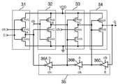
도 3은 본 발명에 의한 누설전류 보상기능을 구비한 티에스피씨 동적 플립플롭의 회로도이다.
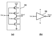
도 4의 (a)는 도 3의 인버터에 대한 상세 회로도이다.
도 4의 (b)는 도 3의 인버터에서 입출력신호 및 제어신호를 나타낸 간략도이다.
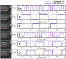
도 5는 본 발명에 의한 TSPC 동적 플립플롭과 종래의 TSPC 동적 플립플롭을 비교 설명하기 위해 시뮬레이션한 결과의 파형도이다.
1 is a circuit diagram of a TS flip flop having a leakage current compensation function according to the related art.
2 is a timing chart of each part of Fig.
3 is a circuit diagram of a TS flip-flop having a leakage current compensation function according to the present invention.
Fig. 4 (a) is a detailed circuit diagram of the inverter of Fig. 3; Fig.
4 (b) is a simplified diagram showing input and output signals and control signals in the inverter of FIG. 3. FIG.
FIG. 5 is a waveform diagram of a result of a simulation to compare a TSPC dynamic flip flop according to the present invention and a conventional TSPC dynamic flip flop.
이하, 첨부한 도면을 참조하여 본 발명의 바람직한 실시예를 상세히 설명하면 다음과 같다.Hereinafter, preferred embodiments of the present invention will be described in detail with reference to the accompanying drawings.
도 3은 본 발명의 실시예에 의한 누설전류 보상기능을 구비한 티에스피씨 동적 플립플롭의 회로도로서 이에 도시한 바와 같이, 제1로직부(31), 제2로직부(32), 제3로직부(33), 출력부(34) 및 누설전류 보상부(35)를 포함한다.3 is a circuit diagram of a DSC dynamic flip-flop having a leakage current compensation function according to an embodiment of the present invention. As shown in FIG. 3, the
제1 로직부(31)는 전원단자(VDD)와 접지단자의 사이에 직렬접속된 제1,2 피모스 트랜지스터(PM1),(PM2) 및 제1 엔모스 트랜지스터(NM1)를 구비하여, 상기 제1 피모스 트랜지스터(PM1) 및 제1 엔모스 트랜지스터(NM1)의 게이트에 공급되는 데이터(D)와 상기 제2 피모스 트랜지스터(PM2)의 게이트에 공급되는 클럭신호(clk)에 따른 로직값을 상기 제2 피모스 트랜지스터(PM2)의 타측 단자와 상기 제1 엔모스 트랜지스터(NM1)의 일측단자의 공통접속 노드인 A 노드에 출력한다. The
제2 로직부(32)는 전원단자(VDD)와 접지단자의 사이에 직렬접속된 제3 피모스 트랜지스터(PM3) 및 제2,3 엔모스 트랜지스터(NM2),(NM3)를 구비하여, 상기 A 노드로부터 상기 제2 엔모스 트랜지스터(NM2)의 게이트에 공급되는 로직값과 상기 제3 피모스 트랜지스터(PM3)의 게이트에 공급되는 클럭신호(clk)에 따른 로직값을 상기 제3 피모스 트랜지스터(PM3)의 타측 단자와 상기 제2 엔모스 트랜지스터(NM2)의 일측단자의 공통접속 노드인 B 노드에 출력한다. The
제3 로직부(33)는 전원단자(VDD)와 접지단자의 사이에 직렬접속된 제4 피모스 트랜지스터(PM4) 및 제4,5 엔모스 트랜지스터(NM4),(NM5)를 구비하여, 상기 B 노드로부터 상기 제4 피모스 트랜지스터(PM4) 및 제5 엔모스 트랜지스터(NM5)의 게이트에 공급되는 로직값과 상기 제4 엔모스 트랜지스터(NM4)의 게이트에 공급되는 클럭신호(clk)에 따른 로직값을 상기 제4 피모스 트랜지스터(PM4)의 타측 단자와 상기 제4 엔모스 트랜지스터(NM4)의 일측단자의 공통접속 노드인 C 노드에 출력한다. The
출력부(34)는 전원단자(VDD)와 접지단자의 사이에 직렬접속된 제5 피모스 트랜지스터(PM5) 및 제6 엔모스 트랜지스터(NM6)를 구비하여, 상기 C 노드로부터 상기 제5 피모스 트랜지스터(PM5) 및 제6 엔모스 트랜지스터(NM6)의 게이트에 공급되는 로직 값에 따라 상기 제5 피모스 트랜지스터(PM5)의 타측 단자와 상기 제6 엔모스 트랜지스터(NM6)의 일측 단자의 공통 접속점 노드인 Q 노드(출력 노드)에 해당 데이터를 출력한다.The
누설전류 보상부(35)는 제1 인버터(36A),제2 인버터(36B) 및 제3 인버터(36C)를 구비하여 상기 A,B,C 노드가 플로팅 상태에 있을 때 이후 단 노드의 로직값을 이전 단의 노드로 피드백하여 누설전류에 의한 오동작이 방지된다. The leakage
먼저, 제1로직부(31), 제2로직부(32), 제3로직부(33) 및 출력부(34)의 동작원리는 통상의 티에스피씨 동적 플립플롭의 동작원리와 유사한 것으로, 이에 대하여 설명하면 다음과 같다. The operation principle of the
제1로직부(31)에서, 제1 피모스 트랜지스터(PM1) 및 제1 엔모스 트랜지스터(NM1)의 게이트에 공급되는 데이터(D)가 "1"일 때, A 노드의 로직값은 "0"이 된다. 제2 피모스 트랜지스터(PM2)의 게이트에 공급되는 클럭신호(clk)의 로직값이 "0"일 때 상기 A 노드의 로직값은 상기 데이터(D)의 반전된 값이 된다. 클럭신호(clk)의 로직값이 "1"이고, 상기 데이터(D)의 로직값이 "0"일 때 상기 A 노드는 플로팅(floating)되어 이전의 로직값을 유지(저장)한다. When the data D supplied to the gates of the first PMOS transistor PM1 and the first NMOS transistor NM1 is "1" in the
제2 로직부(32)에서, 제3 피모스 트랜지스터(PM3) 및 제3 엔모스 트랜지스터(NM3)의 게이트에 공급되는 클럭신호(clk)의 로직값이 "0"일 때 B 노드의 로직값은 "1"이다. 상기 클럭신호(clk)의 로직값이 "1"이고, 상기 A 노드로부터 제2 엔모스 트랜지스터(NM2)의 게이트에 공급되는 로직값이 "1"일 때 상기 B 노드의 로직값은 "0"이다. 상기 A 노드의 로직값이 "0"일 때 상기 B 노드는 플로팅(floating)되어 이전의 로직값을 유지한다. When the logic value of the clock signal clk supplied to the gates of the third PMOS transistor PM3 and the third NMOS transistor NM3 is "0" in the
제3 로직부(13)에서, 제4 피모스 트랜지스터(PM4) 및 제5 엔모스 트랜지스터(NM5)의 게이트에 공급되는 상기 B 노드의 로직값이 "0"일 때 상기 C 노드의 로직값은 "1"이다. 제4 엔모스 트랜지스터(NM4)의 게이트에 공급되는 상기 클럭신호(clk)의 로직값이 "1"일 때 상기 C 노드의 로직값은 상기 B 노드의 로직값의 반전된 로직값이 된다. 상기 클럭신호(clk)의 로직값이 "0"이고, 상기 B 노드의 로직값이 "1"일 때 상기 C 노드는 플로팅되어 이전의 로직값을 유지한다.In the
출력부(14)에서, 상기 C 노드로부터 제5 피모스 트랜지스터(PM5) 및 제6 엔모스 트랜지스터(NM6)의 게이트에 공급되는 로직값의 반전된 로직값이 Q 노드에 출력된다.In the
결국, 상기 설명에서와 같이 상기 A 내지 C 노드는 플로팅 구간에 이전의 로직값을 저장하고, 이렇게 저장된 로직값이 상기 Q 노드 측으로 순차적으로 전달되어 클럭신호(clk)의 한 주기 동안 저장된다. As a result, as described above, the A to C nodes store the previous logic value in the floating interval, and the stored logic value is sequentially transmitted to the Q node side and is stored for one period of the clock signal clk.
상기 설명에서와 같이 상기 A 노드의 플로팅 구간은 클럭신호(clk)의 로직값이 "1"이고, 상기 데이터(D)의 로직값이 "0"일 때이며, B 노드의 로직값과 반전된 값을 가진다. 상기 B 노드의 플로팅 구간은 클럭신호(clk)의 로직값이 "1"이고, 상기 A 노드의 로직값이 "0"일 때이며, C 노드의 로직값과 반전된 값을 가진다. 상기 C 노드의 플로팅 구간은 클럭신호(clk)의 로직값이 "0"이고, 상기 B 노드의 로직값이 "1"일 때이며, Q 노드의 로직값과 반전된 값을 가진다. As described above, the floating period of the node A is when the logic value of the clock signal clk is "1 ", the logic value of the data D is" 0 ", and the logic value of the node B and the inverted value . The floating period of the B-node is when the logic value of the clock signal clk is "1", the logic value of the A-node is "0", and the logic value of the C-node is inverted. The floating period of the C node is when the logic value of the clock signal clk is "0 ", the logic value of the B node is" 1 ", and the logic value of the Q node is inverted.
상기 A,B,C 노드의 각 플로팅 구간은 클럭신호(clk)와 바로 이전 단 노드의 로직값에 의해 결정되고, 상기 결정된 로직값은 다음 단의 노드값과 반전된 값을 가진다. Each floating interval of the nodes A, B, and C is determined by the clock signal clk and the logic value of the immediately preceding node, and the determined logic value has a value inverted from the next node value.
한편, 상기 누설전류 보상부(35)에 의해 상기 A,B,C 노드의 누설전류가 보상(억제)되는데, 이에 대하여 상세히 설명하면 다음과 같다.Meanwhile, the leakage
상기 누설전류 보상부(35)는 제1-3 인버터(36A-36C)를 구비하는데, 도 4의 (a)는 상기 제1-3 인버터(36A-36C)를 CMOS 트랜지스터로 구현한 예를 나타낸 것이다. The leakage
도 4의 (a)를 참조하면, 인버터(35)는 전원단자(VDD)와 접지단자의 사이에 직렬접속된 제6,7 피모스 트랜지스터(PM6,PM7) 및 제7,8엔모스 트랜지스터(NM7,NM8)를 구비한다. 상기 제6 피모스 트랜지스터(PM6)의 게이트와 상기 제8 엔모스 트랜지스터(NM8)의 게이트에 입력전압(Vin)이 공급된다. 상기 제7 피모스 트랜지스터(PM7)의 게이트에는 제어신호(a)가 공급되고, 상기 제7 엔모스 트랜지스터(NM7)의 게이트에 제어신호(b)가 공급된다. 상기 제7피모스 트랜지스터(PM7)의 타측 단자와 상기 제7 엔모스 트랜지스터(NM7)의 일측 단자의 공통접속점으로부터 출력전압(Vout)이 발생된다.4A, the
도 4의 (b)는 상기 도 4의 (a)를 블록도로 표현한 것으로, 여기서 "a"는 상기 제7피모스 트랜지스터(PM7)의 게이트에 공급되는 제어신호로서 상기 도 3에서 데이터(D), 노드신호(A) 및 클럭신호(clk) 중 하나에 해당된다. 그리고, "b"는 상기 제7엔모스 트랜지스터(NM7)의 게이트에 공급되는 제어신호로서 상기 도 3에서 노드신호(B) 및 클럭신호(clk) 중 하나에 해당된다.4 (b) is a block diagram of FIG. 4 (a). Here, "a" is a control signal supplied to the gate of the seventh PMOS transistor PM7, The node signal A, and the clock signal clk. "B" corresponds to one of the node signal B and the clock signal clk in FIG. 3 as a control signal supplied to the gate of the seventh NMOS transistor NM7.
상기 도 4의 (a)에 도시한 인버터(35)의 동작은 아래의 [표 1]에 도시한 진리표와 같다. 예를 들어, 제어신호(a)의 로직값은 '0'이고, 제어신호(b)의 로직값은 '1'인 경우 출력전압(Vout)의 로직값은 입력전압(Vin)의 반전된 로직값이 된다. 입력전압(Vin), 제어신호(a)(b)의 로직값이 모두 '0'인 경우 출력전압(Vout)의 로직값은 '1'이 된다. 입력전압(Vin), 제어신호(a)(b)의 로직값이 모두 '1'인 경우 출력전압(Vout)의 로직값은 '0'이 된다. 나머지의 경우 출력전압(Vout)의 단자는 오픈(Open)상태(High Impedance = High-Z)가 된다. The operation of the
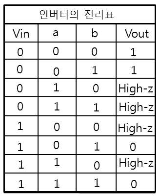
아래의 [표 2]는 상기 도 3에 도시된 티에스피씨 동적 플립플롭(30)의 진리표를 나타낸 것이다. Table 2 below shows a truth table of the TS flip flop 30 shown in FIG.

제1-3 인버터(36A-36C)를 이용하여 상기 A,B,C 노드의 누설전류를 보상하는 동작을 설명하면 다음과 같다. The operation of compensating the leakage currents of the nodes A, B, and C using the first to
A 노드가 플로팅 상태에 놓여 있을 때, B 노드는 플로팅 상태가 아니다. 이와 같은 상태에서 입력데이터(D)와 클럭신호(clk)를 제1 인버터(36A)의 제어신호로 사용하여 A 노드의 반전된 로직값을 갖는 B 노드의 신호를 상기 제1 인버터(36A)를 통해 A 노드로 피드백시킨다. 이렇게 함으로써, 상기 A 노드가 상기 B 노드의 반전된 신호(예: "1")로 구동되어 A 노드의 기생커패시터에 저장된 전하량이 누설전류에 의해 줄어드는 것이 보상된다.When node A is in a floating state, node B is not in a floating state. In this state, the input data D and the clock signal clk are used as the control signal of the
B 노드가 플로팅 상태에 놓여 있을 때, C 노드는 플로팅 상태가 아니다. 이와 같은 상태에서 A 노드의 신호와 클럭신호(clk)를 제2 인버터(36B)의 제어신호로 사용하여 B 노드의 반전된 로직값을 갖는 C 노드의 신호를 상기 제2 인버터(36B)를 통해 B 노드로 피드백시킨다. 이렇게 함으로써, 상기 B 노드가 상기 C 노드의 반전된 신호(예: "1")로 구동되어 B 노드의 기생커패시터에 저장된 전하량이 누설전류에 의해 줄어드는 것이 보상된다.When the B node is in the floating state, the C node is not in the floating state. In this state, the signal of the node A and the clock signal clk are used as the control signal of the
C 노드가 플로팅 상태에 놓여 있을 때, B 노드는 플로팅 상태가 아니다. 이와 같은 상태에서 B 노드의 신호와 클럭신호(clk)를 제3 인버터(36C)의 제어신호로 사용하여 Q 노드의 신호를 상기 제3 인버터(36C)를 통해 C 노드로 피드백시킨다. 이렇게 함으로써, 상기 C 노드가 상기 Q 노드의 반전된 신호(예: "1")로 구동되어 C 노드의 기생커패시터에 저장된 전하량이 누설전류에 의해 줄어드는 것이 보상된다.When the C node is in the floating state, the B node is not in the floating state. In this state, the signal of the node B and the clock signal clk are used as the control signal of the
상기 누설전류 보상부(35)는 상기 [표 1]의 설명에서와 같이 상기 A 내지 C 노드 중 해당 노드가 플로팅 상태이거나, 입력신호 및 제어신호가 모두 "0" 또는 "1"인 경우에만 동작하고, 나머지 경우에는 오픈상태(High-Z)가 되므로 TSPC 동적 플립플롭(30)의 동작에 영향을 미치지 않는다. 또한, 상기 누설전류 보상부(35)는 TSPC 동적 플립플롭(30)에서 자신을 제외한 부분과 병렬로 연결되므로 TSPC 동적 플립플롭(30)의 동작속도에 아무런 영향을 미치지 않는다. The leakage
도 5는 종래의 TSPC 동적 플립플롭과 본 발명에 의한 TSPC 동적 플립플롭(30)에 대하여 클럭신호(clk)의 주파수가 1 MHz인 조건에서 시뮬레이션한 결과를 나타낸 파형도이다. 도 5에 도시된 바와 같이, 종래의 TSPC 동적 플립플롭은 누설전류에 의해 오동작하는 반면, 본 발명에 의한 TSPC 동적 플립플롭은 정상적으로 동작하는 것을 알 수 있다. 5 is a waveform diagram showing a result of simulation for a conventional TSPC dynamic flip-flop and a TSPC dynamic flip-flop 30 according to the present invention under the condition that the frequency of the clock signal clk is 1 MHz. As shown in FIG. 5, the conventional TSPC dynamic flip flop malfunctions due to the leakage current, whereas the TSPC dynamic flip flop according to the present invention operates normally.
아래의 [표 3]은 종래 기술에 의한 TSPC 동적 플립플롭과 본 발명에 의한 TSPC 동적 플립플롭에 대한 셋업 타임, 홀드 타임, 입출력 지연시간 및 전력소모량을 비교 분석한 시뮬레이션 결과이다. 이에 도시한 바와 같이 본 발명에 의한 누설전류 보상기능을 구비한 티에스피씨 동적 플립플롭이 종래 기술에 의한 TSPC 동적 플립플롭보다 전력 소모량이 8.8% 정도 증가되었지만 성능의 변화는 거의 없는 것을 알 수 있다. Table 3 below shows the simulation results of a comparative analysis of setup time, hold time, input / output delay time, and power consumption for the TSPC dynamic flip-flop according to the prior art and the TSPC dynamic flip-flop according to the present invention. As shown in the figure, the power consumption of the DSC dynamic flip-flop having the leakage current compensation function according to the present invention is 8.8% higher than that of the TSPC dynamic flip-flop according to the related art.

이상에서 본 발명의 바람직한 실시예에 대하여 상세히 설명하였지만, 본 발명의 권리범위가 이에 한정되는 것이 아니라 다음의 청구범위에서 정의하는 본 발명의 기본 개념을 바탕으로 보다 다양한 실시예로 구현될 수 있으며, 이러한 실시예들 또한 본 발명의 권리범위에 속하는 것이다.
Although the preferred embodiments of the present invention have been described in detail above, it should be understood that the scope of the present invention is not limited thereto. These embodiments are also within the scope of the present invention.
31 : 제1로직부 32 : 제2로직부
33 : 제3로직부 34 : 출력부
35 : 누설전류 보상부 36A : 제1 인버터
36B : 제2 인버터 36C : 제3 인버터31: first logic unit 32: second logic unit
33: third logic section 34: output section
35: Leakage current compensating
36B:
Claims (7)
상기 전원단자와 접지단자의 사이에 순차적으로 직렬접속된 제3 피모스 트랜지스터 및 제2,3 엔모스 트랜지스터를 구비하여, 상기 클럭신호와 상기 A 노드로부터 공급되는 신호에 따른 로직값을 상기 제3 피모스 트랜지스터의 타측 단자와 상기 제2 엔모스 트랜지스터의 일측단자의 공통접속 노드인 B 노드에 출력하는 제2로직부;
상기 전원단자와 접지단자의 사이에 순차적으로 직렬접속된 제4 피모스 트랜지스터 및 제4,5 엔모스 트랜지스터를 구비하여, 상기 B 노드로부터 공급되는 신호와 상기 클럭신호에 따른 로직값을 상기 제4 피모스 트랜지스터의 타측 단자와 상기 제4 엔모스 트랜지스터의 일측단자의 공통접속 노드인 C 노드에 출력하는 제3로직부;
상기 전원단자와 접지단자의 사이에 순차적으로 직렬접속된 제5 피모스 트랜지스터 및 제6 엔모스 트랜지스터를 구비하여, 상기 C 노드로부터 공급되는 로직 값에 따라 상기 제5 피모스 트랜지스터의 타측 단자와 상기 제6 엔모스 트랜지스터의 일측 단자의 공통 접속점 노드인 Q 노드에 해당 데이터를 출력하는 출력부; 및
상기 제1-3 로직부의 A 내지 C 노드 중 임의의 노드가 플로팅 상태에 있을 때, 해당 노드의 논리값과 반대 논리값을 갖는 후단 노드의 신호를 해당 노드로 피드백시켜 해당 노드의 누설전류를 보상하는 누설전류 보상부;를 포함하는 것을 특징으로 하는 누설전류 보상기능을 구비한 티에스피씨 동적 플립플롭.
And first and second PMOS transistors serially connected in series between a power supply terminal and a ground terminal, wherein a logic value according to input data and a clock signal is connected to the other terminal of the second PMOS transistor To a node A which is a common connection node of one terminal of the first NMOS transistor;
And a third PMOS transistor and a second and third NMOS transistors serially connected in series between the power supply terminal and the ground terminal, wherein the logic value according to the clock signal and the signal supplied from the A node, A second logic section for outputting the other terminal of the PMOS transistor to a node B which is a common connection node of one terminal of the second NMOS transistor;
And a fourth PMOS transistor and fourth and fifth NMOS transistors serially connected in series between the power supply terminal and the ground terminal, wherein a signal supplied from the B node and a logic value according to the clock signal are supplied to the fourth A third logic section for outputting the other terminal of the PMOS transistor to a node C which is a common connection node of one terminal of the fourth NMOS transistor;
And a fifth PMOS transistor and a sixth NMOS transistor serially connected in series between the power supply terminal and the ground terminal, wherein the other terminal of the fifth PMOS transistor and the second terminal of the fifth PMOS transistor, An output section for outputting the corresponding data to a Q node which is a node of a common node of one terminal of the sixth MOS transistor; And
When any one of nodes A to C of the first to third logic units is in a floating state, a signal of a rear node having a logic value opposite to that of the corresponding node is fed back to the corresponding node, And a leakage current compensating unit for compensating a leakage current of the TS flip flop.
2. The TS dynamic flip-flop according to claim 1, wherein a signal of a rear-end node that feeds back the leakage current compensating section to the corresponding node has a logic value of "1 ".
상기 A 노드가 플로팅 상태일 때, 상기 입력데이터와 상기 클럭신호의 제어를 받아 상기 A 노드의 반전된 로직값을 갖는 상기 B 노드의 신호를 상기 A 노드로 피드백시키는 제1 인버터;
상기 B 노드가 플로팅 상태일 때, 상기 A 노드의 신호와 상기 클럭신호의 제어를 받아 상기 B 노드의 반전된 로직값을 갖는 상기 C 노드의 신호를 상기 B 노드로 피드백시키는 제2 인버터; 및
상기 C 노드가 플로팅 상태일 때, 상기 B 노드의 신호와 상기 클럭신호의 제어를 받아 상기 Q 노드의 신호를 상기 상기 C 노드로 피드백시키는 제3 인버터를 포함하는 것을 특징으로 하는 누설전류 보상기능을 구비한 티에스피씨 동적 플립플롭.
The apparatus of claim 1, wherein the leakage current compensation unit
A first inverter for receiving the signal of the node B having the inverted logic value of the node A, and feeding the signal of the node B to the node A under the control of the input data and the clock signal when the node A is in a floating state;
A second inverter for receiving the signal of the node A and the clock signal to feed back the signal of the node C having the inverted logic value of the node B to the node B when the node B is in a floating state; And
And a third inverter for receiving the signal of the B node and the clock signal to feed back the signal of the Q node to the C node when the C node is in a floating state. Equipped TS flip flop.
4. The inverter of claim 3, wherein the first to third inverters include an inverter having a sixth and seventh PMOS transistors and a seventh and eighth NMOS transistors serially connected in series between a power supply terminal and a ground terminal , The inverter is supplied with the input voltage to the gate of the sixth PMOS transistor and the gate of the eighth NMOS transistor, and the respective control signals are supplied to the gates of the seventh PMOS transistor and the seventh NMOS transistor And an output voltage is generated from a common connection point between the other terminal of the seventh PMOS transistor and one terminal of the seventh NMOS transistor.
The apparatus of claim 3, wherein the first inverter has an input terminal connected to the B node, an output terminal connected to the A node, a terminal of the input data connected to one control terminal, And the terminal of the signal is connected to the terminal of the TS flipflop.
4. The method of claim 3, wherein the second inverter has an input terminal connected to the C node, an output terminal connected to the B node, the A node connected to one control terminal, And the terminal is connected to the terminal of the TS flip flop.
Priority Applications (1)
| Application Number | Priority Date | Filing Date | Title |
|---|---|---|---|
| KR1020120146304A KR20140077464A (en) | 2012-12-14 | 2012-12-14 | Tspc dynamic flip flop having leakage current compensation function |
Applications Claiming Priority (1)
| Application Number | Priority Date | Filing Date | Title |
|---|---|---|---|
| KR1020120146304A KR20140077464A (en) | 2012-12-14 | 2012-12-14 | Tspc dynamic flip flop having leakage current compensation function |
Publications (1)
| Publication Number | Publication Date |
|---|---|
| KR20140077464A true KR20140077464A (en) | 2014-06-24 |
Family
ID=51129399
Family Applications (1)
| Application Number | Title | Priority Date | Filing Date |
|---|---|---|---|
| KR1020120146304A Ceased KR20140077464A (en) | 2012-12-14 | 2012-12-14 | Tspc dynamic flip flop having leakage current compensation function |
Country Status (1)
| Country | Link |
|---|---|
| KR (1) | KR20140077464A (en) |
Cited By (7)
| Publication number | Priority date | Publication date | Assignee | Title |
|---|---|---|---|---|
| CN105162438A (en) * | 2015-09-28 | 2015-12-16 | 东南大学 | TSPC (True Single Phase Clock) type data flip-flop (DFF) capable of reducing glitch |
| CN109756207A (en) * | 2018-11-21 | 2019-05-14 | 西北工业大学 | A kind of TSPC edge triggered flip flop with automatic feedback gated clock |
| CN110677141A (en) * | 2019-09-30 | 2020-01-10 | 杭州嘉楠耘智信息科技有限公司 | Dynamic D flip-flops, data operation units, chips, computing power boards and computing equipment |
| CN110690887A (en) * | 2019-09-30 | 2020-01-14 | 杭州嘉楠耘智信息科技有限公司 | Dynamic latch, data operation unit, chip, computing power board and computing equipment |
| CN110708041A (en) * | 2019-09-30 | 2020-01-17 | 杭州嘉楠耘智信息科技有限公司 | Electric leakage feedback dynamic D trigger, data operation unit, chip, force calculation board and computing equipment |
| CN110706731A (en) * | 2019-09-30 | 2020-01-17 | 杭州嘉楠耘智信息科技有限公司 | Electric leakage compensation dynamic register, data arithmetic unit, chip, force calculation board and computing equipment |
| CN111769826A (en) * | 2020-06-19 | 2020-10-13 | 易兆微电子(杭州)股份有限公司 | TSPC trigger with setting and resetting functions |
-
2012
- 2012-12-14 KR KR1020120146304A patent/KR20140077464A/en not_active Ceased
Cited By (9)
| Publication number | Priority date | Publication date | Assignee | Title |
|---|---|---|---|---|
| CN105162438A (en) * | 2015-09-28 | 2015-12-16 | 东南大学 | TSPC (True Single Phase Clock) type data flip-flop (DFF) capable of reducing glitch |
| CN109756207A (en) * | 2018-11-21 | 2019-05-14 | 西北工业大学 | A kind of TSPC edge triggered flip flop with automatic feedback gated clock |
| CN110677141A (en) * | 2019-09-30 | 2020-01-10 | 杭州嘉楠耘智信息科技有限公司 | Dynamic D flip-flops, data operation units, chips, computing power boards and computing equipment |
| CN110690887A (en) * | 2019-09-30 | 2020-01-14 | 杭州嘉楠耘智信息科技有限公司 | Dynamic latch, data operation unit, chip, computing power board and computing equipment |
| CN110708041A (en) * | 2019-09-30 | 2020-01-17 | 杭州嘉楠耘智信息科技有限公司 | Electric leakage feedback dynamic D trigger, data operation unit, chip, force calculation board and computing equipment |
| CN110706731A (en) * | 2019-09-30 | 2020-01-17 | 杭州嘉楠耘智信息科技有限公司 | Electric leakage compensation dynamic register, data arithmetic unit, chip, force calculation board and computing equipment |
| KR20220073770A (en) * | 2019-09-30 | 2022-06-03 | 항저우 가나안 인텔리전스 인포메이션 테크놀로지 컴퍼니 리미티드 | Earth leakage compensation dynamic registers, data operation units, chips, hash boards and computing devices |
| CN111769826A (en) * | 2020-06-19 | 2020-10-13 | 易兆微电子(杭州)股份有限公司 | TSPC trigger with setting and resetting functions |
| CN111769826B (en) * | 2020-06-19 | 2023-11-07 | 易兆微电子(杭州)股份有限公司 | TSPC trigger with setting and resetting functions |
Similar Documents
| Publication | Publication Date | Title |
|---|---|---|
| US8742796B2 (en) | Low energy flip-flops | |
| KR20140077464A (en) | Tspc dynamic flip flop having leakage current compensation function | |
| CN105471410B (en) | Flip-flop with low clock power | |
| US7772883B2 (en) | Level shifter | |
| US6856558B1 (en) | Integrated circuit devices having high precision digital delay lines therein | |
| US6798249B2 (en) | Circuit for asynchronous reset in current mode logic circuits | |
| US20080074151A1 (en) | Dual-edge-triggered, clock-gated logic circuit and method | |
| US8797077B2 (en) | Master-slave flip-flop circuit | |
| US9350325B2 (en) | Reduced dynamic power D flip-flop | |
| US8405424B2 (en) | Output buffer with adjustable feedback | |
| US20170257080A1 (en) | Low-area low clock-power flip-flop | |
| KR20060053741A (en) | High speed flip-flop | |
| US7528630B2 (en) | High speed flip-flop | |
| US8593193B1 (en) | Complementary semi-dynamic D-type flip-flop | |
| US8063685B1 (en) | Pulsed flip-flop circuit | |
| US6700425B1 (en) | Multi-phase clock generators that utilize differential signals to achieve reduced setup and hold times | |
| CN114095004B (en) | Driving circuit | |
| JP2012023533A (en) | Level converter circuit | |
| CN220627412U (en) | Input data pre-alignment circuit for semiconductor memory | |
| EP2184852B1 (en) | Latch circuit including data input terminal and scan data input terminal, and semiconductor device and control method | |
| WO2002080179A2 (en) | Digital leakage compensation circuit | |
| KR101880491B1 (en) | Low power time amplifier and method for operating the same | |
| US9537489B1 (en) | Level shifter with dynamic bias technique under overstress voltage | |
| US8928380B2 (en) | Current-mode D latch with reset function and associated circuit | |
| CN101465631A (en) | Delay circuit |
Legal Events
| Date | Code | Title | Description |
|---|---|---|---|
| A201 | Request for examination | ||
| PA0109 | Patent application |
Patent event code: PA01091R01D Comment text: Patent Application Patent event date: 20121214 |
|
| PA0201 | Request for examination | ||
| E902 | Notification of reason for refusal | ||
| PE0902 | Notice of grounds for rejection |
Comment text: Notification of reason for refusal Patent event date: 20140306 Patent event code: PE09021S01D |
|
| E601 | Decision to refuse application | ||
| PE0601 | Decision on rejection of patent |
Patent event date: 20140520 Comment text: Decision to Refuse Application Patent event code: PE06012S01D Patent event date: 20140306 Comment text: Notification of reason for refusal Patent event code: PE06011S01I |
|
| PG1501 | Laying open of application |