KR20140077499A - 저항 변화 메모리 장치 및 그 제조방법 - Google Patents
저항 변화 메모리 장치 및 그 제조방법 Download PDFInfo
- Publication number
- KR20140077499A KR20140077499A KR1020120146380A KR20120146380A KR20140077499A KR 20140077499 A KR20140077499 A KR 20140077499A KR 1020120146380 A KR1020120146380 A KR 1020120146380A KR 20120146380 A KR20120146380 A KR 20120146380A KR 20140077499 A KR20140077499 A KR 20140077499A
- Authority
- KR
- South Korea
- Prior art keywords
- gate
- forming
- pillar
- semiconductor substrate
- shunt
- Prior art date
- Legal status (The legal status is an assumption and is not a legal conclusion. Google has not performed a legal analysis and makes no representation as to the accuracy of the status listed.)
- Withdrawn
Links
Images


Classifications
-
- H—ELECTRICITY
- H10—SEMICONDUCTOR DEVICES; ELECTRIC SOLID-STATE DEVICES NOT OTHERWISE PROVIDED FOR
- H10N—ELECTRIC SOLID-STATE DEVICES NOT OTHERWISE PROVIDED FOR
- H10N70/00—Solid-state devices having no potential barriers, and specially adapted for rectifying, amplifying, oscillating or switching
- H10N70/20—Multistable switching devices, e.g. memristors
-
- H—ELECTRICITY
- H10—SEMICONDUCTOR DEVICES; ELECTRIC SOLID-STATE DEVICES NOT OTHERWISE PROVIDED FOR
- H10B—ELECTRONIC MEMORY DEVICES
- H10B63/00—Resistance change memory devices, e.g. resistive RAM [ReRAM] devices
- H10B63/30—Resistance change memory devices, e.g. resistive RAM [ReRAM] devices comprising selection components having three or more electrodes, e.g. transistors
- H10B63/34—Resistance change memory devices, e.g. resistive RAM [ReRAM] devices comprising selection components having three or more electrodes, e.g. transistors of the vertical channel field-effect transistor type
-
- H—ELECTRICITY
- H10—SEMICONDUCTOR DEVICES; ELECTRIC SOLID-STATE DEVICES NOT OTHERWISE PROVIDED FOR
- H10B—ELECTRONIC MEMORY DEVICES
- H10B63/00—Resistance change memory devices, e.g. resistive RAM [ReRAM] devices
- H10B63/80—Arrangements comprising multiple bistable or multi-stable switching components of the same type on a plane parallel to the substrate, e.g. cross-point arrays
-
- H—ELECTRICITY
- H10—SEMICONDUCTOR DEVICES; ELECTRIC SOLID-STATE DEVICES NOT OTHERWISE PROVIDED FOR
- H10B—ELECTRONIC MEMORY DEVICES
- H10B99/00—Subject matter not provided for in other groups of this subclass
-
- H—ELECTRICITY
- H10—SEMICONDUCTOR DEVICES; ELECTRIC SOLID-STATE DEVICES NOT OTHERWISE PROVIDED FOR
- H10D—INORGANIC ELECTRIC SEMICONDUCTOR DEVICES
- H10D30/00—Field-effect transistors [FET]
- H10D30/60—Insulated-gate field-effect transistors [IGFET]
- H10D30/63—Vertical IGFETs
-
- H—ELECTRICITY
- H10—SEMICONDUCTOR DEVICES; ELECTRIC SOLID-STATE DEVICES NOT OTHERWISE PROVIDED FOR
- H10N—ELECTRIC SOLID-STATE DEVICES NOT OTHERWISE PROVIDED FOR
- H10N70/00—Solid-state devices having no potential barriers, and specially adapted for rectifying, amplifying, oscillating or switching
- H10N70/801—Constructional details of multistable switching devices
- H10N70/821—Device geometry
- H10N70/826—Device geometry adapted for essentially vertical current flow, e.g. sandwich or pillar type devices
-
- H—ELECTRICITY
- H10—SEMICONDUCTOR DEVICES; ELECTRIC SOLID-STATE DEVICES NOT OTHERWISE PROVIDED FOR
- H10N—ELECTRIC SOLID-STATE DEVICES NOT OTHERWISE PROVIDED FOR
- H10N70/00—Solid-state devices having no potential barriers, and specially adapted for rectifying, amplifying, oscillating or switching
- H10N70/801—Constructional details of multistable switching devices
- H10N70/881—Switching materials
- H10N70/882—Compounds of sulfur, selenium or tellurium, e.g. chalcogenides
-
- H—ELECTRICITY
- H10—SEMICONDUCTOR DEVICES; ELECTRIC SOLID-STATE DEVICES NOT OTHERWISE PROVIDED FOR
- H10D—INORGANIC ELECTRIC SEMICONDUCTOR DEVICES
- H10D30/00—Field-effect transistors [FET]
- H10D30/01—Manufacture or treatment
- H10D30/021—Manufacture or treatment of FETs having insulated gates [IGFET]
- H10D30/025—Manufacture or treatment of FETs having insulated gates [IGFET] of vertical IGFETs
-
- H—ELECTRICITY
- H10—SEMICONDUCTOR DEVICES; ELECTRIC SOLID-STATE DEVICES NOT OTHERWISE PROVIDED FOR
- H10D—INORGANIC ELECTRIC SEMICONDUCTOR DEVICES
- H10D64/00—Electrodes of devices having potential barriers
- H10D64/20—Electrodes characterised by their shapes, relative sizes or dispositions
- H10D64/27—Electrodes not carrying the current to be rectified, amplified, oscillated or switched, e.g. gates
- H10D64/311—Gate electrodes for field-effect devices
- H10D64/411—Gate electrodes for field-effect devices for FETs
- H10D64/511—Gate electrodes for field-effect devices for FETs for IGFETs
- H10D64/512—Disposition of the gate electrodes, e.g. buried gates
- H10D64/513—Disposition of the gate electrodes, e.g. buried gates within recesses in the substrate, e.g. trench gates, groove gates or buried gates
-
- H—ELECTRICITY
- H10—SEMICONDUCTOR DEVICES; ELECTRIC SOLID-STATE DEVICES NOT OTHERWISE PROVIDED FOR
- H10D—INORGANIC ELECTRIC SEMICONDUCTOR DEVICES
- H10D64/00—Electrodes of devices having potential barriers
- H10D64/20—Electrodes characterised by their shapes, relative sizes or dispositions
- H10D64/27—Electrodes not carrying the current to be rectified, amplified, oscillated or switched, e.g. gates
- H10D64/311—Gate electrodes for field-effect devices
- H10D64/411—Gate electrodes for field-effect devices for FETs
- H10D64/511—Gate electrodes for field-effect devices for FETs for IGFETs
- H10D64/517—Gate electrodes for field-effect devices for FETs for IGFETs characterised by the conducting layers
- H10D64/518—Gate electrodes for field-effect devices for FETs for IGFETs characterised by the conducting layers characterised by their lengths or sectional shapes
-
- H—ELECTRICITY
- H10—SEMICONDUCTOR DEVICES; ELECTRIC SOLID-STATE DEVICES NOT OTHERWISE PROVIDED FOR
- H10D—INORGANIC ELECTRIC SEMICONDUCTOR DEVICES
- H10D64/00—Electrodes of devices having potential barriers
- H10D64/20—Electrodes characterised by their shapes, relative sizes or dispositions
- H10D64/27—Electrodes not carrying the current to be rectified, amplified, oscillated or switched, e.g. gates
- H10D64/311—Gate electrodes for field-effect devices
- H10D64/411—Gate electrodes for field-effect devices for FETs
- H10D64/511—Gate electrodes for field-effect devices for FETs for IGFETs
- H10D64/517—Gate electrodes for field-effect devices for FETs for IGFETs characterised by the conducting layers
- H10D64/519—Gate electrodes for field-effect devices for FETs for IGFETs characterised by the conducting layers characterised by their top-view geometrical layouts
-
- H—ELECTRICITY
- H10—SEMICONDUCTOR DEVICES; ELECTRIC SOLID-STATE DEVICES NOT OTHERWISE PROVIDED FOR
- H10N—ELECTRIC SOLID-STATE DEVICES NOT OTHERWISE PROVIDED FOR
- H10N70/00—Solid-state devices having no potential barriers, and specially adapted for rectifying, amplifying, oscillating or switching
- H10N70/011—Manufacture or treatment of multistable switching devices
-
- H—ELECTRICITY
- H10—SEMICONDUCTOR DEVICES; ELECTRIC SOLID-STATE DEVICES NOT OTHERWISE PROVIDED FOR
- H10N—ELECTRIC SOLID-STATE DEVICES NOT OTHERWISE PROVIDED FOR
- H10N70/00—Solid-state devices having no potential barriers, and specially adapted for rectifying, amplifying, oscillating or switching
- H10N70/20—Multistable switching devices, e.g. memristors
- H10N70/231—Multistable switching devices, e.g. memristors based on solid-state phase change, e.g. between amorphous and crystalline phases, Ovshinsky effect
-
- H—ELECTRICITY
- H10—SEMICONDUCTOR DEVICES; ELECTRIC SOLID-STATE DEVICES NOT OTHERWISE PROVIDED FOR
- H10N—ELECTRIC SOLID-STATE DEVICES NOT OTHERWISE PROVIDED FOR
- H10N70/00—Solid-state devices having no potential barriers, and specially adapted for rectifying, amplifying, oscillating or switching
- H10N70/801—Constructional details of multistable switching devices
- H10N70/841—Electrodes
- H10N70/8413—Electrodes adapted for resistive heating
Landscapes
- Semiconductor Memories (AREA)
Abstract
상기 반도체 기판상에 일정 간격을 가지고 배열되는 복수의 수직 트랜지스터;
상기 복수의 수직 트랜지스터 상부에 각각 형성되는 저항 변화 영역; 및
인접하는 수직 트랜지스터 사이의 공간에 위치되며, 상기 수직 트랜지스터게이트와 전기적으로 연결되도록 구성되는 션트 게이트를 포함한다.
Description
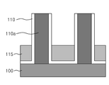
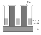
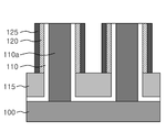
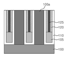
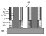
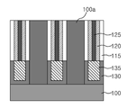
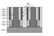
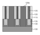
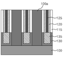
도 2a-도 2b, 도 3a-도 3b, 도 4a-도 4b, 도 5a-도 5b, 도 6a-도 6b, 도 7a-도 7b 및 도 8a-도 8b는 본 발명에 따른 저항 변화 메모리 장치의 제조방법을 공정 순서별로 나타낸 단면도이다.
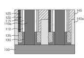
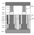
도 9 및 도 10은 본 발명의 다른 실시예에 따른 저항 변화 메모리 장치를 나타낸 단면도들이다.
130 : 게이트 절연막 135 : 메인 게이트
145,145a : 션트 게이트
Claims (14)
- 반도체 기판;
상기 반도체 기판상에 일정 간격을 가지고 배열되는 복수의 수직 트랜지스터;
상기 복수의 수직 트랜지스터 상부에 각각 형성되는 저항 변화 영역; 및
인접하는 수직 트랜지스터 사이의 공간에 위치되며, 상기 수직 트랜지스터의 게이트와 전기적으로 연결되도록 구성되는 션트 게이트를 포함하는 저항 변화 메모리 장치. - 제 1 항에 있어서,
상기 수직 트랜지스터는,
상기 반도체 기판 표면으로 부터 수직 방향으로 연장된 필라; 및
상기 필라의 하부 영역을 둘러싸도록 구성되는 서라운드 게이트를 포함하는 저항 변화 메모리 장치. - 제 2 항에 있어서,
상기 션트 게이트는 인접하는 서라운드 게이트 중 선택되는 하나와 연결되도록 구성되는 저항 변화 메모리 장치. - 제 1 항에 있어서,
상기 션트 게이트는 상기 서라운드 게이트와 콘택되며 상기 반도체 기판과 수직인 방향으로 연장되는 제 1 부분, 및 상기 제 1 부분과 연결되며 상기 반도체 기판 표면과 수평인 방향으로 연장되는 제 2 부분을 포함하는 저항 변화 메모리 장치. - 제 4 항에 있어서,
상기 제 2 부분은 상기 저항 변화 영역 사이의 공간으로 연장되는 저항 변화 메모리 장치. - 제 4 항에 있어서,
상기 제 1 부분과 상기 필라 사이에 절연 스페이서가 개재되는 저항 변화 메모리 장치. - 반도체 기판 상부에 필라 및 상기 필라 하부를 둘러싸는 게이트로 구성되는 수직 트랜지스터를 복수개 형성하는 단계;
상기 게이트 상부의 필라 측벽에 제 1 및 제 2 스페이서를 형성하는 단계;
상기 수직 트랜지스터 사이를 절연막으로 매립하는 단계;
상기 필라 일측부에 위치하는 상기 제 2 스페이서 및 상기 절연막의 상부 영역을 제거하여 공간부를 형성하는 단계; 및
상기 공간부내에 도전물을 매립하여, 션트 게이트를 형성하는 단계를 포함하는 저항 변화 메모리 장치의 제조방법. - 제 7 항에 있어서,
상기 션트 게이트를 형성하는 단계 이후에,
상기 수직 트랜지스터 상부에 가열 전극을 형성하는 단계; 및
상기 가열 전극 상부에 저항 변화층을 형성하는 단계를 더 포함하는 저항 변화 메모리 장치의 제조방법. - 제 7 항에 있어서,
상기 공간부를 형성하는 단계는,
상기 제 2 스페이서 및 상기 절연막 상부 영역에 데미지를 인가하는 단계; 및
상기 데미지가 인가된 제 2 스페이서 및 절연막 상부 영역을 선택적으로 제거하는 단계를 포함하는 저항 변화 메모리 장치의 제조방법. - 제 9 항에 있어서,
상기 제 2 스페이서 및 상기 절연막 상부 영역에 데미지를 인가하는 단계는,
사선 이온 주입 공정을 진행하는 단계인 저항 변화 메모리 장치의 제조방법. - 제 7 항에 있어서,
상기 션트 게이트를 형성하는 단계 이후에,
반도체 기판 결과물 상부에 도전층을 증착하는 단계;
상기 수직 트랜지스터의 사이의 공간에 잔류되도록 상기 도전층을 패터닝하는 단계; 및
상기 도전층 양측의 수직 트랜지스터 상부에 가열 전극 및 저항 변화층을 형성하는 단계를 포함하는 저항 변화 메모리 장치의 제조방법. - 제 11 항에 있어서,
상기 션트 게이트를 형성하는 단계 이후에,
성가 션트 게이트 상부에 추가의 게이트층을 형성하는 단계;및
상기 수직 트랜지스터 상부에 저항 변화 구조물을 형성하는 단계를 더 포함하는 저항 변화 메모리 장치의 제조방법. - 제 12 항에 있어서,
상기 저항 변화 구조물을 형성하는 단계는,
상기 수직 트랜지스터 상부에 가열 전극을 형성하는 단계; 및
상기 가열 전극 상부에 저항 변화 물질층을 형성하는 단계를 포함하는 저항 변화 메모리 장치의 제조방법. - 채널 필라를 서라운드하는 게이트; 및
상기 채널 필라 사이에 위치되며 인접하는 게이트 중 하나와 연결되어 상기 게이트의 면적을 연장시키는 션트 게이트를 포함하는 반도체 메모리 장치.
Priority Applications (5)
| Application Number | Priority Date | Filing Date | Title |
|---|---|---|---|
| KR1020120146380A KR20140077499A (ko) | 2012-12-14 | 2012-12-14 | 저항 변화 메모리 장치 및 그 제조방법 |
| US13/795,872 US8981448B2 (en) | 2012-12-14 | 2013-03-12 | Variable resistance memory device with shunt gate connected to corresponding gate |
| CN201310221335.1A CN103872067B (zh) | 2012-12-14 | 2013-06-05 | 可变电阻存储器件及其制造方法 |
| US14/617,607 US9331124B2 (en) | 2012-12-14 | 2015-02-09 | Variable resistance memory device and method of manufacturing the same |
| US15/074,913 US9620566B2 (en) | 2012-12-14 | 2016-03-18 | Variable resistance memory device with shunt gate connected to corresponding gate |
Applications Claiming Priority (1)
| Application Number | Priority Date | Filing Date | Title |
|---|---|---|---|
| KR1020120146380A KR20140077499A (ko) | 2012-12-14 | 2012-12-14 | 저항 변화 메모리 장치 및 그 제조방법 |
Publications (1)
| Publication Number | Publication Date |
|---|---|
| KR20140077499A true KR20140077499A (ko) | 2014-06-24 |
Family
ID=50910435
Family Applications (1)
| Application Number | Title | Priority Date | Filing Date |
|---|---|---|---|
| KR1020120146380A Withdrawn KR20140077499A (ko) | 2012-12-14 | 2012-12-14 | 저항 변화 메모리 장치 및 그 제조방법 |
Country Status (3)
| Country | Link |
|---|---|
| US (3) | US8981448B2 (ko) |
| KR (1) | KR20140077499A (ko) |
| CN (1) | CN103872067B (ko) |
Cited By (1)
| Publication number | Priority date | Publication date | Assignee | Title |
|---|---|---|---|---|
| KR20220019590A (ko) * | 2020-08-10 | 2022-02-17 | 솔브레인 주식회사 | 식각 조성물 및 이를 이용한 반도체 소자의 제조방법 |
Families Citing this family (18)
| Publication number | Priority date | Publication date | Assignee | Title |
|---|---|---|---|---|
| JP5692886B1 (ja) * | 2013-04-19 | 2015-04-01 | ユニサンティス エレクトロニクス シンガポール プライベート リミテッドUnisantis Electronics Singapore Pte Ltd. | 半導体装置の製造方法、及び、半導体装置 |
| KR20150020847A (ko) * | 2013-08-19 | 2015-02-27 | 에스케이하이닉스 주식회사 | 3차원 반도체 장치, 이를 구비하는 저항 변화 메모리 장치, 및 그 제조방법 |
| WO2015075819A1 (ja) * | 2013-11-22 | 2015-05-28 | ユニサンティス エレクトロニクス シンガポール プライベート リミテッド | 半導体装置、及び半導体装置の製造方法 |
| JP6226765B2 (ja) * | 2014-02-07 | 2017-11-08 | 株式会社東芝 | 半導体素子、半導体素子の製造方法、および半導体装置 |
| KR20160006466A (ko) * | 2014-07-09 | 2016-01-19 | 에스케이하이닉스 주식회사 | 수직 채널을 갖는 반도체 집적 회로 장치 및 그 제조방법 |
| CN105448989B (zh) * | 2014-08-26 | 2018-12-25 | 中芯国际集成电路制造(上海)有限公司 | 半导体装置及其制造方法 |
| TWI559586B (zh) * | 2014-12-31 | 2016-11-21 | 力晶科技股份有限公司 | 電阻式隨機存取記憶體及其製造方法 |
| MA42103A (fr) * | 2015-05-18 | 2018-03-28 | Bayer Pharma AG | Régime posologique à base de modulateur sélectif du récepteur de la progestérone (rpm) |
| KR102527669B1 (ko) * | 2016-08-11 | 2023-05-02 | 삼성전자주식회사 | 가변 저항 메모리 장치 및 그 제조 방법 |
| KR102375588B1 (ko) * | 2017-07-06 | 2022-03-16 | 삼성전자주식회사 | 반도체 장치 및 그 제조 방법 |
| US10796833B2 (en) | 2018-09-25 | 2020-10-06 | International Business Machines Corporation | Magnetic tunnel junction with low series resistance |
| US10957850B2 (en) * | 2018-10-04 | 2021-03-23 | International Business Machines Corporation | Multi-layer encapsulation to enable endpoint-based process control for embedded memory fabrication |
| US10903424B2 (en) * | 2019-05-07 | 2021-01-26 | International Business Machines Corporation | Resistive RAM cell structure for gradual set programming |
| US11145816B2 (en) | 2019-12-20 | 2021-10-12 | International Business Machines Corporation | Resistive random access memory cells integrated with vertical field effect transistor |
| US11588104B2 (en) | 2021-06-14 | 2023-02-21 | International Business Machines Corporation | Resistive memory with vertical transport transistor |
| CN117835693A (zh) * | 2022-09-27 | 2024-04-05 | 华为技术有限公司 | 一种存储阵列、存储器及电子设备 |
| KR20240066636A (ko) * | 2022-11-08 | 2024-05-16 | 에스케이하이닉스 주식회사 | 반도체 장치 및 그 제조방법 |
| CN117425352A (zh) * | 2022-12-19 | 2024-01-19 | 北京超弦存储器研究院 | 半导体器件、电子设备 |
Family Cites Families (17)
| Publication number | Priority date | Publication date | Assignee | Title |
|---|---|---|---|---|
| US4553041A (en) * | 1983-08-22 | 1985-11-12 | Motorola, Inc. | Monolithic zero crossing triac driver |
| US5010386A (en) * | 1989-12-26 | 1991-04-23 | Texas Instruments Incorporated | Insulator separated vertical CMOS |
| JPH06268173A (ja) * | 1993-03-15 | 1994-09-22 | Toshiba Corp | 半導体記憶装置 |
| US5965924A (en) * | 1995-11-22 | 1999-10-12 | Cypress Semiconductor Corp. | Metal plug local interconnect |
| US7023009B2 (en) * | 1997-10-01 | 2006-04-04 | Ovonyx, Inc. | Electrically programmable memory element with improved contacts |
| US6304483B1 (en) * | 1998-02-24 | 2001-10-16 | Micron Technology, Inc. | Circuits and methods for a static random access memory using vertical transistors |
| JP2001094094A (ja) * | 1999-09-21 | 2001-04-06 | Hitachi Ltd | 半導体装置およびその製造方法 |
| WO2002072803A2 (en) * | 2001-03-09 | 2002-09-19 | The Government Of The United States Of America, As Represented By The Secretary, Department Of Health And Human Services | Subgenomic replicons of the flavivirus dengue |
| US6759702B2 (en) * | 2002-09-30 | 2004-07-06 | International Business Machines Corporation | Memory cell with vertical transistor and trench capacitor with reduced burried strap |
| JP4064955B2 (ja) * | 2004-09-30 | 2008-03-19 | 株式会社東芝 | 半導体装置及びその製造方法 |
| JP2009071247A (ja) * | 2007-09-18 | 2009-04-02 | Elpida Memory Inc | 半導体記憶装置 |
| KR100908819B1 (ko) * | 2007-11-02 | 2009-07-21 | 주식회사 하이닉스반도체 | 수직채널트랜지스터를 구비한 반도체소자 및 그 제조 방법 |
| JP2010225259A (ja) * | 2009-02-27 | 2010-10-07 | Renesas Electronics Corp | 半導体装置 |
| KR101033468B1 (ko) * | 2009-06-30 | 2011-05-09 | 주식회사 하이닉스반도체 | 워드 라인의 저항을 개선할 수 있는 상변화 메모리 장치, 그것의 배열 구조, 및 그것의 제조방법 |
| KR101811308B1 (ko) | 2010-11-10 | 2017-12-27 | 삼성전자주식회사 | 저항 변화 체를 갖는 비 휘발성 메모리 소자 및 그 제조방법 |
| JP2012204399A (ja) * | 2011-03-23 | 2012-10-22 | Toshiba Corp | 抵抗変化メモリ |
| KR20130077374A (ko) * | 2011-12-29 | 2013-07-09 | 에스케이하이닉스 주식회사 | 가변 저항 메모리 장치 및 그 제조 방법 |
-
2012
- 2012-12-14 KR KR1020120146380A patent/KR20140077499A/ko not_active Withdrawn
-
2013
- 2013-03-12 US US13/795,872 patent/US8981448B2/en active Active
- 2013-06-05 CN CN201310221335.1A patent/CN103872067B/zh active Active
-
2015
- 2015-02-09 US US14/617,607 patent/US9331124B2/en active Active
-
2016
- 2016-03-18 US US15/074,913 patent/US9620566B2/en active Active
Cited By (1)
| Publication number | Priority date | Publication date | Assignee | Title |
|---|---|---|---|---|
| KR20220019590A (ko) * | 2020-08-10 | 2022-02-17 | 솔브레인 주식회사 | 식각 조성물 및 이를 이용한 반도체 소자의 제조방법 |
Also Published As
| Publication number | Publication date |
|---|---|
| US9331124B2 (en) | 2016-05-03 |
| US20140166971A1 (en) | 2014-06-19 |
| CN103872067B (zh) | 2018-06-15 |
| US20150155335A1 (en) | 2015-06-04 |
| US8981448B2 (en) | 2015-03-17 |
| CN103872067A (zh) | 2014-06-18 |
| US20160204163A1 (en) | 2016-07-14 |
| US9620566B2 (en) | 2017-04-11 |
Similar Documents
| Publication | Publication Date | Title |
|---|---|---|
| KR20140077499A (ko) | 저항 변화 메모리 장치 및 그 제조방법 | |
| US9450023B1 (en) | Vertical bit line non-volatile memory with recessed word lines | |
| US9818798B2 (en) | Vertical thin film transistors in non-volatile storage systems | |
| US9443910B1 (en) | Silicided bit line for reversible-resistivity memory | |
| CN107221545B (zh) | 三维电阻式存储器及其制造方法 | |
| US9391269B2 (en) | Variable resistance memory devices | |
| US8890110B2 (en) | Vertical memory device and method of fabricating the same | |
| US20140248763A1 (en) | Vertical Bit Line Non-Volatile Memory Systems And Methods Of Fabrication | |
| US9018610B2 (en) | Resistive memory device and method of manufacturing the same | |
| CN104766925A (zh) | 通过在HK HfO之前沉积Ti覆盖层改善RRAM的数据保持 | |
| US12446228B2 (en) | Memory device and method for fabricating the same | |
| TWI755123B (zh) | 記憶體裝置及用於製造其之方法 | |
| TW201419450A (zh) | 記憶胞、記憶體陣列及於記憶體陣列中形成選擇電晶體之方法 | |
| KR101860946B1 (ko) | 3차원 입체 구조를 가지는 비휘발성 메모리 | |
| US9425239B2 (en) | Vertical transistor for resistive memory | |
| KR100980295B1 (ko) | 상변환 기억 소자의 제조방법 | |
| KR100929633B1 (ko) | 상변화 기억 소자 | |
| KR101155093B1 (ko) | 반도체 메모리 장치 | |
| TW202221919A (zh) | 具有最佳化電阻層之記憶體 | |
| KR20070063811A (ko) | 상변환 기억 소자 및 그의 제조방법 | |
| KR20090114149A (ko) | 상변화 기억 소자 및 그의 제조방법 | |
| KR20090026679A (ko) | 상변화 기억 소자의 제조방법 | |
| KR20070063810A (ko) | 상변환 기억 소자 및 그의 제조방법 |
Legal Events
| Date | Code | Title | Description |
|---|---|---|---|
| PA0109 | Patent application |
St.27 status event code: A-0-1-A10-A12-nap-PA0109 |
|
| PN2301 | Change of applicant |
St.27 status event code: A-3-3-R10-R13-asn-PN2301 St.27 status event code: A-3-3-R10-R11-asn-PN2301 |
|
| PG1501 | Laying open of application |
St.27 status event code: A-1-1-Q10-Q12-nap-PG1501 |
|
| PN2301 | Change of applicant |
St.27 status event code: A-3-3-R10-R13-asn-PN2301 St.27 status event code: A-3-3-R10-R11-asn-PN2301 |
|
| PC1203 | Withdrawal of no request for examination |
St.27 status event code: N-1-6-B10-B12-nap-PC1203 |
|
| WITN | Application deemed withdrawn, e.g. because no request for examination was filed or no examination fee was paid | ||
| P22-X000 | Classification modified |
St.27 status event code: A-2-2-P10-P22-nap-X000 |
|
| P22-X000 | Classification modified |
St.27 status event code: A-2-2-P10-P22-nap-X000 |
|
| P22-X000 | Classification modified |
St.27 status event code: A-2-2-P10-P22-nap-X000 |
|
| P22-X000 | Classification modified |
St.27 status event code: A-2-2-P10-P22-nap-X000 |