KR20140087645A - 포지티브형 감광성 수지 조성물 - Google Patents
포지티브형 감광성 수지 조성물 Download PDFInfo
- Publication number
- KR20140087645A KR20140087645A KR1020120158168A KR20120158168A KR20140087645A KR 20140087645 A KR20140087645 A KR 20140087645A KR 1020120158168 A KR1020120158168 A KR 1020120158168A KR 20120158168 A KR20120158168 A KR 20120158168A KR 20140087645 A KR20140087645 A KR 20140087645A
- Authority
- KR
- South Korea
- Prior art keywords
- unsubstituted
- substituted
- group
- meth
- compound
- Prior art date
- Legal status (The legal status is an assumption and is not a legal conclusion. Google has not performed a legal analysis and makes no representation as to the accuracy of the status listed.)
- Ceased
Links
Classifications
-
- G—PHYSICS
- G03—PHOTOGRAPHY; CINEMATOGRAPHY; ANALOGOUS TECHNIQUES USING WAVES OTHER THAN OPTICAL WAVES; ELECTROGRAPHY; HOLOGRAPHY
- G03F—PHOTOMECHANICAL PRODUCTION OF TEXTURED OR PATTERNED SURFACES, e.g. FOR PRINTING, FOR PROCESSING OF SEMICONDUCTOR DEVICES; MATERIALS THEREFOR; ORIGINALS THEREFOR; APPARATUS SPECIALLY ADAPTED THEREFOR
- G03F7/00—Photomechanical, e.g. photolithographic, production of textured or patterned surfaces, e.g. printing surfaces; Materials therefor, e.g. comprising photoresists; Apparatus specially adapted therefor
- G03F7/004—Photosensitive materials
- G03F7/039—Macromolecular compounds which are photodegradable, e.g. positive electron resists
- G03F7/0392—Macromolecular compounds which are photodegradable, e.g. positive electron resists the macromolecular compound being present in a chemically amplified positive photoresist composition
-
- G—PHYSICS
- G03—PHOTOGRAPHY; CINEMATOGRAPHY; ANALOGOUS TECHNIQUES USING WAVES OTHER THAN OPTICAL WAVES; ELECTROGRAPHY; HOLOGRAPHY
- G03F—PHOTOMECHANICAL PRODUCTION OF TEXTURED OR PATTERNED SURFACES, e.g. FOR PRINTING, FOR PROCESSING OF SEMICONDUCTOR DEVICES; MATERIALS THEREFOR; ORIGINALS THEREFOR; APPARATUS SPECIALLY ADAPTED THEREFOR
- G03F7/00—Photomechanical, e.g. photolithographic, production of textured or patterned surfaces, e.g. printing surfaces; Materials therefor, e.g. comprising photoresists; Apparatus specially adapted therefor
- G03F7/004—Photosensitive materials
- G03F7/022—Quinonediazides
- G03F7/0223—Iminoquinonediazides; Para-quinonediazides
-
- G—PHYSICS
- G03—PHOTOGRAPHY; CINEMATOGRAPHY; ANALOGOUS TECHNIQUES USING WAVES OTHER THAN OPTICAL WAVES; ELECTROGRAPHY; HOLOGRAPHY
- G03F—PHOTOMECHANICAL PRODUCTION OF TEXTURED OR PATTERNED SURFACES, e.g. FOR PRINTING, FOR PROCESSING OF SEMICONDUCTOR DEVICES; MATERIALS THEREFOR; ORIGINALS THEREFOR; APPARATUS SPECIALLY ADAPTED THEREFOR
- G03F7/00—Photomechanical, e.g. photolithographic, production of textured or patterned surfaces, e.g. printing surfaces; Materials therefor, e.g. comprising photoresists; Apparatus specially adapted therefor
- G03F7/004—Photosensitive materials
- G03F7/022—Quinonediazides
- G03F7/0226—Quinonediazides characterised by the non-macromolecular additives
-
- G—PHYSICS
- G03—PHOTOGRAPHY; CINEMATOGRAPHY; ANALOGOUS TECHNIQUES USING WAVES OTHER THAN OPTICAL WAVES; ELECTROGRAPHY; HOLOGRAPHY
- G03F—PHOTOMECHANICAL PRODUCTION OF TEXTURED OR PATTERNED SURFACES, e.g. FOR PRINTING, FOR PROCESSING OF SEMICONDUCTOR DEVICES; MATERIALS THEREFOR; ORIGINALS THEREFOR; APPARATUS SPECIALLY ADAPTED THEREFOR
- G03F7/00—Photomechanical, e.g. photolithographic, production of textured or patterned surfaces, e.g. printing surfaces; Materials therefor, e.g. comprising photoresists; Apparatus specially adapted therefor
- G03F7/004—Photosensitive materials
- G03F7/039—Macromolecular compounds which are photodegradable, e.g. positive electron resists
- G03F7/0392—Macromolecular compounds which are photodegradable, e.g. positive electron resists the macromolecular compound being present in a chemically amplified positive photoresist composition
- G03F7/0397—Macromolecular compounds which are photodegradable, e.g. positive electron resists the macromolecular compound being present in a chemically amplified positive photoresist composition the macromolecular compound having an alicyclic moiety in a side chain
-
- G—PHYSICS
- G03—PHOTOGRAPHY; CINEMATOGRAPHY; ANALOGOUS TECHNIQUES USING WAVES OTHER THAN OPTICAL WAVES; ELECTROGRAPHY; HOLOGRAPHY
- G03F—PHOTOMECHANICAL PRODUCTION OF TEXTURED OR PATTERNED SURFACES, e.g. FOR PRINTING, FOR PROCESSING OF SEMICONDUCTOR DEVICES; MATERIALS THEREFOR; ORIGINALS THEREFOR; APPARATUS SPECIALLY ADAPTED THEREFOR
- G03F7/00—Photomechanical, e.g. photolithographic, production of textured or patterned surfaces, e.g. printing surfaces; Materials therefor, e.g. comprising photoresists; Apparatus specially adapted therefor
- G03F7/004—Photosensitive materials
- G03F7/09—Photosensitive materials characterised by structural details, e.g. supports, auxiliary layers
- G03F7/095—Photosensitive materials characterised by structural details, e.g. supports, auxiliary layers having more than one photosensitive layer
- G03F7/0952—Photosensitive materials characterised by structural details, e.g. supports, auxiliary layers having more than one photosensitive layer comprising silver halide or silver salt based image forming systems, e.g. for camera speed exposure
-
- H—ELECTRICITY
- H10—SEMICONDUCTOR DEVICES; ELECTRIC SOLID-STATE DEVICES NOT OTHERWISE PROVIDED FOR
- H10P—GENERIC PROCESSES OR APPARATUS FOR THE MANUFACTURE OR TREATMENT OF DEVICES COVERED BY CLASS H10
- H10P76/00—Manufacture or treatment of masks on semiconductor bodies, e.g. by lithography or photolithography
- H10P76/20—Manufacture or treatment of masks on semiconductor bodies, e.g. by lithography or photolithography of masks comprising organic materials
- H10P76/204—Manufacture or treatment of masks on semiconductor bodies, e.g. by lithography or photolithography of masks comprising organic materials of organic photoresist masks
Landscapes
- Physics & Mathematics (AREA)
- Spectroscopy & Molecular Physics (AREA)
- General Physics & Mathematics (AREA)
- Engineering & Computer Science (AREA)
- Architecture (AREA)
- Structural Engineering (AREA)
- Materials For Photolithography (AREA)
Abstract
Description


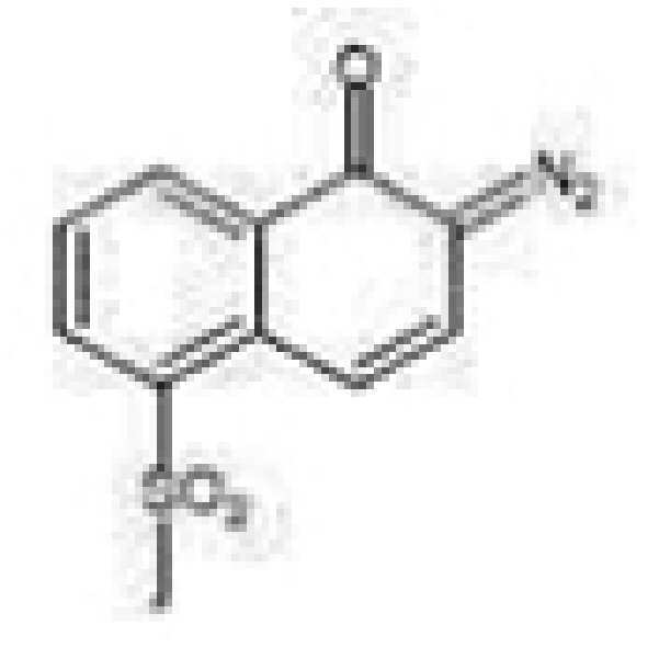

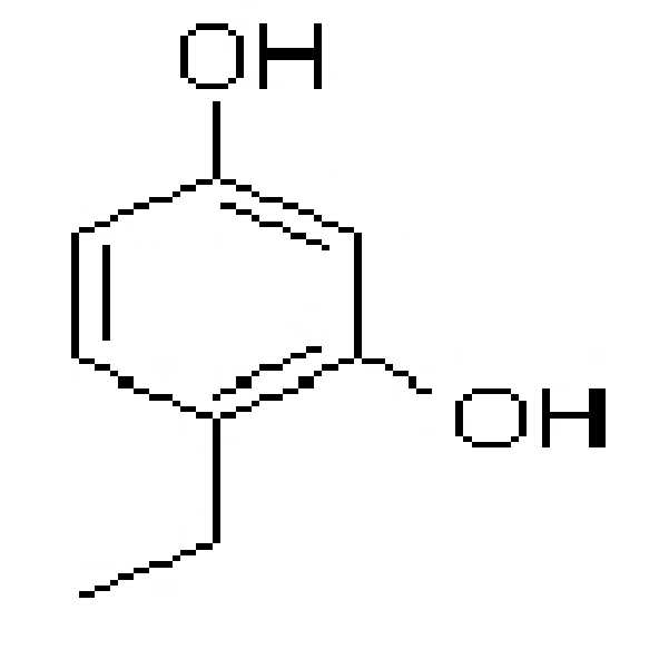
| 원료 |
투입량 (중량부) | ||||||
| 비교예 1 | 실시예 1 | 실시예 2 | 실시예 3 | 실시예 4 | 실시예 5 | 실시예 6 | |
| 알칼리 가용성 수지 (PBO 전구체) |
100 | 100 | 100 | 100 | 100 | 100 | 100 |
| Ebecryl220 (Cytec 사제) |
- | 10 | 20 | - | - | - | - |
| Ebecryl230 (Cytec 사제) |
- | - | - | 10 | 20 | - | - |
| Ebecryl290 (Cytec 사제) |
- | - | - | - | - | 10 | 20 |
| 디아조퀴논 화합물 |
10 | 10 | 10 | 10 | 10 | 10 | 10 |
| 실란 화합물 | 0.2 | 0.2 | 0.2 | 0.2 | 0.2 | 0.2 | 0.2 |
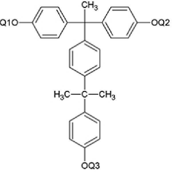
| 페놀 화합물 | 7.5 | 7.5 | 7.5 | 7.5 | 7.5 | 7.5 | 7.5 |
| PGME | 250 | 250 | 250 | 250 | 250 | 250 | 250 |
| GBL | 100 | 100 | 100 | 100 | 100 | 100 | 100 |
| 구분 | 잔막율 | 감도 | 내열성 | 패턴밀착성 | 유전율 |
| 비교예 1 | ○ | ○ | △ | X | ○ |
| 실시예 1 | ○ | ○ | ○ | ○ | ○ |
| 실시예 2 | ○ | ○ | ○ | ○ | ○ |
| 실시예 3 | ○ | ○ | ○ | ○ | ○ |
| 실시예 4 | ○ | ○ | ○ | ○ | ○ |
| 실시예 5 | ○ | ○ | ○ | ○ | ○ |
| 실시예 6 | ○ | ○ | ○ | ○ | ○ |
Claims (10)
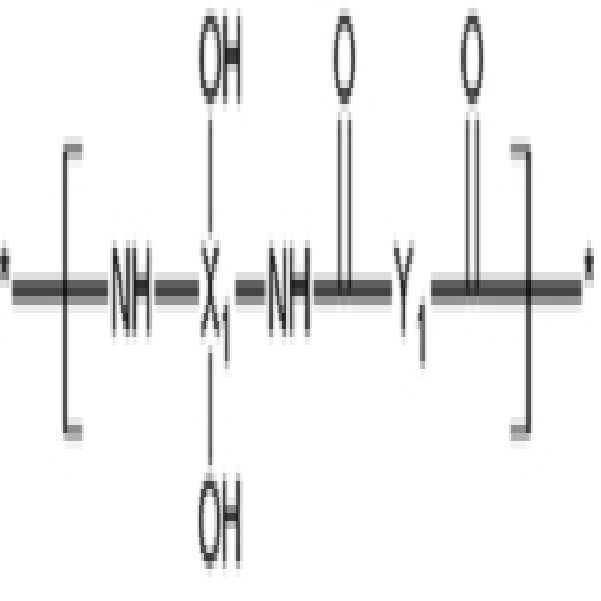
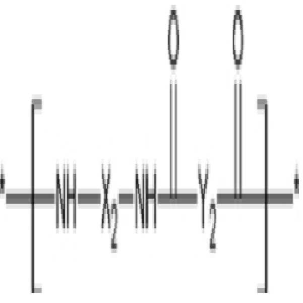
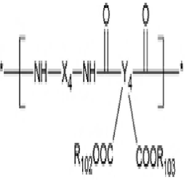
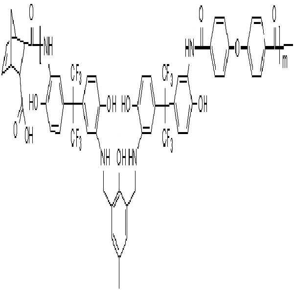
- (A) 폴리벤조옥사졸 전구체, 폴리이미드 전구체, 및 이들의 조합에서 선택되는 알칼리 가용성 수지;
(B) 감광성 디아조퀴아논 화합물;
(C) 다관능성 우레탄 (메타)아크릴레이트 화합물; 및
(D) 용매
를 포함하는 포지티브형 감광성 수지 조성물. - 제1항에 있어서,
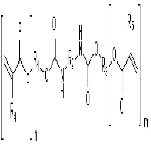
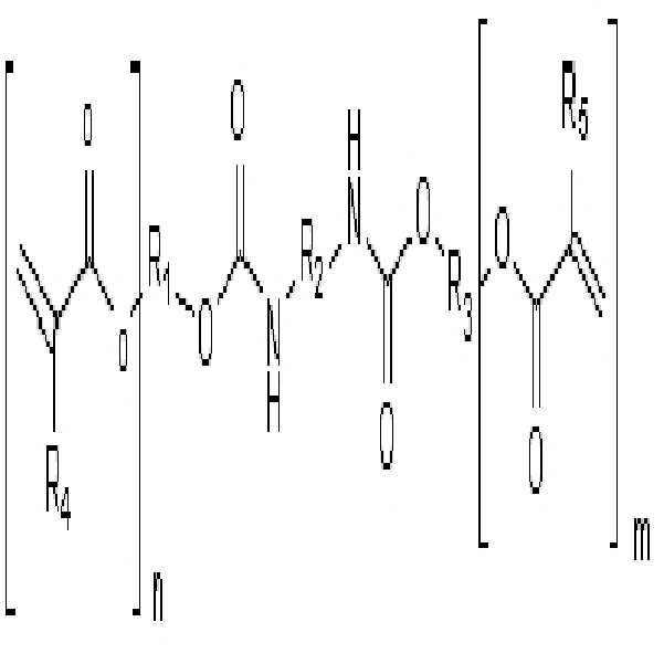
상기 다관능성 우레탄 (메타)아크릴레이트 화합물이 하기 화학식 1로 표시되는 것인 포지티브형 감광성 수지 조성물:
(화학식 1)

상기 화학식 1에서,
상기 R1과 R3은 동일하거나 상이할 수 있으며, 각각 독립적으로 치환 또는 비치환된 C1 내지 C30의 알킬렌기, 치환 또는 비치환된 C6 내지 C30의 사이클로알킬렌기, 치환 또는 비치환된 C3 내지 C30의 헤테로사이클로알킬렌기, 치환 또는 비치환된 C6 내지 C30 아릴렌기, 치환 또는 비치환된 C7 내지 C30 알킬 아릴렌기, 또는 치환 또는 비치환된 C3 내지 C30의 헤테로아릴렌기이며,
상기 R2는 치환 또는 비치환된 C1 내지 C30의 알킬렌기, 치환 또는 비치환된 C6 내지 C30의 사이클로알킬렌기, 치환 또는 비치환된 C3 내지 C30의 헤테로사이클로알킬렌기, 치환 또는 비치환된 C6 내지 C30 아릴렌기, 치환 또는 비치환된 C7 내지 C30 알킬 아릴렌기, 또는 치환 또는 비치환된 C3 내지 C30의 헤테로아릴렌기이고,
상기 R4와 R5는 각각 독립적으로 수소 또는 메틸기이며,
상기 n 및 m 은 각각 1 내지 3의 정수 중 하나이며, 서로 같거나 다를 수 있다. - 제1항에 있어서,
상기 다관능성 우레탄 (메타)아크릴레이트 화합물이 하기 화학식 2로 표시되는 것인 포지티브형 감광성 수지 조성물:
(화학식 2)

- 제1항에 있어서,
상기 다관능성 우레탄 (메타)아크릴레이트 화합물의 분자량은 내지 5,000 grams/mole 인 포지티브형 감광성 수지 조성물. - 제1항에 있어서,
상기 조성물은,
(A) 상기 알칼리 가용성 수지 100 중량부에 대해,
(B) 상기 감광성 디아조퀴아논 화합물 5 내지 100 중량부;
(C) 상기 다관능성 우레탄 (메타)아크릴레이트 화합물 5 내지 40 중량부; 및
(D) 용매 100 내지 400 중량부
를 포함하는 것인 포지티브형 감광성 수지 조성물. - 제5항에 있어서,
상기 (C) 다관능성 우레탄 (메타)아크릴레이트 화합물이 10 내지 20 중량부로 포함된 포지티브형 감광성 수지 조성물. - 제1항에 있어서,
페놀 화합물을 추가로 포함하는 포지티브형 감광성 수지 조성물. - 제1항에 있어서,
실란 화합물을 추가로 포함하는 포지티브형 감광성 수지 조성물. - 제1항 내지 제8항 중 어느 한 항의 포지티브형 감광성 수지 조성물을 이용하여 형성된 절연막.
- 제9항의 절연막을 포함하는 표시소자.
Priority Applications (1)
| Application Number | Priority Date | Filing Date | Title |
|---|---|---|---|
| KR1020120158168A KR20140087645A (ko) | 2012-12-31 | 2012-12-31 | 포지티브형 감광성 수지 조성물 |
Applications Claiming Priority (1)
| Application Number | Priority Date | Filing Date | Title |
|---|---|---|---|
| KR1020120158168A KR20140087645A (ko) | 2012-12-31 | 2012-12-31 | 포지티브형 감광성 수지 조성물 |
Publications (1)
| Publication Number | Publication Date |
|---|---|
| KR20140087645A true KR20140087645A (ko) | 2014-07-09 |
Family
ID=51736532
Family Applications (1)
| Application Number | Title | Priority Date | Filing Date |
|---|---|---|---|
| KR1020120158168A Ceased KR20140087645A (ko) | 2012-12-31 | 2012-12-31 | 포지티브형 감광성 수지 조성물 |
Country Status (1)
| Country | Link |
|---|---|
| KR (1) | KR20140087645A (ko) |
Cited By (3)
| Publication number | Priority date | Publication date | Assignee | Title |
|---|---|---|---|---|
| KR20160108108A (ko) * | 2015-03-06 | 2016-09-19 | 삼성에스디아이 주식회사 | 차광막을 포함하는 디바이스 및 상기 차광막 패터닝 방법 |
| JP2017090803A (ja) * | 2015-11-16 | 2017-05-25 | 東京応化工業株式会社 | 層間絶縁膜形成用感光性樹脂組成物、層間絶縁膜及び層間絶縁膜の形成方法、並びにデバイス |
| KR20210057104A (ko) * | 2018-10-19 | 2021-05-20 | 후지필름 가부시키가이샤 | 경화막의 제조 방법, 수지 조성물, 경화막, 적층체의 제조 방법 및 반도체 디바이스의 제조 방법 |
-
2012
- 2012-12-31 KR KR1020120158168A patent/KR20140087645A/ko not_active Ceased
Cited By (3)
| Publication number | Priority date | Publication date | Assignee | Title |
|---|---|---|---|---|
| KR20160108108A (ko) * | 2015-03-06 | 2016-09-19 | 삼성에스디아이 주식회사 | 차광막을 포함하는 디바이스 및 상기 차광막 패터닝 방법 |
| JP2017090803A (ja) * | 2015-11-16 | 2017-05-25 | 東京応化工業株式会社 | 層間絶縁膜形成用感光性樹脂組成物、層間絶縁膜及び層間絶縁膜の形成方法、並びにデバイス |
| KR20210057104A (ko) * | 2018-10-19 | 2021-05-20 | 후지필름 가부시키가이샤 | 경화막의 제조 방법, 수지 조성물, 경화막, 적층체의 제조 방법 및 반도체 디바이스의 제조 방법 |
Similar Documents
| Publication | Publication Date | Title |
|---|---|---|
| JP5410918B2 (ja) | ポジティブ型感光性樹脂組成物 | |
| KR101423177B1 (ko) | 포지티브형 감광성 수지 조성물 | |
| KR101400186B1 (ko) | 포지티브형 감광성 수지 조성물, 이를 사용하여 제조된 감광성 수지막 및 상기 감광성 수지막을 포함하는 반도체 소자 | |
| KR20130078782A (ko) | 포지티브형 감광성 수지 조성물 | |
| KR20090056737A (ko) | 포지티브형 감광성 수지 조성물 | |
| KR20150117567A (ko) | 포지티브형 감광성 수지 조성물, 감광성 수지막, 및 이를 이용한 표시 소자 | |
| KR20120078325A (ko) | 포지티브형 감광성 수지 조성물, 이를 사용하여 제조된 감광성 수지막 및 상기 감광성 수지막을 포함하는 반도체 소자 | |
| KR101423539B1 (ko) | 포지티브형 감광성 수지 조성물 | |
| KR101400187B1 (ko) | 포지티브형 감광성 수지 조성물, 이를 사용하여 제조된 감광성 수지막 및 상기 감광성 수지막을 포함하는 반도체 소자 | |
| KR102670213B1 (ko) | 포지티브형 감광성 수지 조성물, 포지티브형 감광성 드라이 필름, 포지티브형 감광성 드라이 필름의 제조 방법, 패턴 형성 방법, 경화 피막 형성 방법, 층간 절연막, 표면 보호막, 및 전자 부품 | |
| KR20140087645A (ko) | 포지티브형 감광성 수지 조성물 | |
| JP2011053679A (ja) | ポジ型感光性組成物 | |
| KR101311940B1 (ko) | 포지티브형 감광성 수지 조성물 | |
| KR20140086733A (ko) | 포지티브형 감광성 수지 조성물, 이를 이용한 절연막 및 상기 절연막을 포함하는 표시 소자 | |
| KR101015859B1 (ko) | 포지티브형 감광성 수지 조성물 | |
| KR101333690B1 (ko) | 포지티브형 감광성 수지 조성물 | |
| KR20140086724A (ko) | 표시장치 절연막용 감광성 수지 조성물, 및 이를 이용한 표시장치 절연막 및 표시장치 | |
| KR101413078B1 (ko) | 포지티브형 감광성 수지 조성물 | |
| KR101257696B1 (ko) | 포지티브형 감광성 수지 조성물 | |
| KR101247624B1 (ko) | 포지티브형 감광성 수지 조성물 | |
| KR101333693B1 (ko) | 포지티브형 감광성 수지 조성물 | |
| KR101400190B1 (ko) | 포지티브형 감광성 수지 조성물, 이를 포함하는 감광성 수지막 및 상기 감광성 수지막을 포함하는 반도체 소자 | |
| KR20120066923A (ko) | 신규 페놀 화합물 및 이를 포함하는 포지티브형 감광성 수지 조성물 | |
| KR101400188B1 (ko) | 포지티브형 감광성 수지 조성물, 이를 포함하는 감광성 수지막 및 상기 감광성 수지막을 포함하는 반도체 소자 | |
| KR102302050B1 (ko) | 감광성 수지 조성물, 이를 이용한 감광성 수지막 및 전자 소자 |
Legal Events
| Date | Code | Title | Description |
|---|---|---|---|
| PA0109 | Patent application |
St.27 status event code: A-0-1-A10-A12-nap-PA0109 |
|
| PN2301 | Change of applicant |
St.27 status event code: A-3-3-R10-R13-asn-PN2301 St.27 status event code: A-3-3-R10-R11-asn-PN2301 |
|
| A201 | Request for examination | ||
| PA0201 | Request for examination |
St.27 status event code: A-1-2-D10-D11-exm-PA0201 |
|
| PG1501 | Laying open of application |
St.27 status event code: A-1-1-Q10-Q12-nap-PG1501 |
|
| D13-X000 | Search requested |
St.27 status event code: A-1-2-D10-D13-srh-X000 |
|
| D14-X000 | Search report completed |
St.27 status event code: A-1-2-D10-D14-srh-X000 |
|
| E902 | Notification of reason for refusal | ||
| PE0902 | Notice of grounds for rejection |
St.27 status event code: A-1-2-D10-D21-exm-PE0902 |
|
| E902 | Notification of reason for refusal | ||
| PE0902 | Notice of grounds for rejection |
St.27 status event code: A-1-2-D10-D21-exm-PE0902 |
|
| E601 | Decision to refuse application | ||
| PE0601 | Decision on rejection of patent |
St.27 status event code: N-2-6-B10-B15-exm-PE0601 |
|
| P22-X000 | Classification modified |
St.27 status event code: A-2-2-P10-P22-nap-X000 |