KR20140089014A - 표시 장치 및 그 제조 방법 - Google Patents
표시 장치 및 그 제조 방법 Download PDFInfo
- Publication number
- KR20140089014A KR20140089014A KR1020120158589A KR20120158589A KR20140089014A KR 20140089014 A KR20140089014 A KR 20140089014A KR 1020120158589 A KR1020120158589 A KR 1020120158589A KR 20120158589 A KR20120158589 A KR 20120158589A KR 20140089014 A KR20140089014 A KR 20140089014A
- Authority
- KR
- South Korea
- Prior art keywords
- light
- light source
- light guide
- layer
- display
- Prior art date
- Legal status (The legal status is an assumption and is not a legal conclusion. Google has not performed a legal analysis and makes no representation as to the accuracy of the status listed.)
- Ceased
Links
Images






Classifications
-
- G—PHYSICS
- G02—OPTICS
- G02B—OPTICAL ELEMENTS, SYSTEMS OR APPARATUS
- G02B6/00—Light guides; Structural details of arrangements comprising light guides and other optical elements, e.g. couplings
- G02B6/0001—Light guides; Structural details of arrangements comprising light guides and other optical elements, e.g. couplings specially adapted for lighting devices or systems
- G02B6/0011—Light guides; Structural details of arrangements comprising light guides and other optical elements, e.g. couplings specially adapted for lighting devices or systems the light guides being planar or of plate-like form
- G02B6/0013—Means for improving the coupling-in of light from the light source into the light guide
- G02B6/0015—Means for improving the coupling-in of light from the light source into the light guide provided on the surface of the light guide or in the bulk of it
- G02B6/002—Means for improving the coupling-in of light from the light source into the light guide provided on the surface of the light guide or in the bulk of it by shaping at least a portion of the light guide, e.g. with collimating, focussing or diverging surfaces
- G02B6/0021—Means for improving the coupling-in of light from the light source into the light guide provided on the surface of the light guide or in the bulk of it by shaping at least a portion of the light guide, e.g. with collimating, focussing or diverging surfaces for housing at least a part of the light source, e.g. by forming holes or recesses
-
- G—PHYSICS
- G02—OPTICS
- G02F—OPTICAL DEVICES OR ARRANGEMENTS FOR THE CONTROL OF LIGHT BY MODIFICATION OF THE OPTICAL PROPERTIES OF THE MEDIA OF THE ELEMENTS INVOLVED THEREIN; NON-LINEAR OPTICS; FREQUENCY-CHANGING OF LIGHT; OPTICAL LOGIC ELEMENTS; OPTICAL ANALOGUE/DIGITAL CONVERTERS
- G02F1/00—Devices or arrangements for the control of the intensity, colour, phase, polarisation or direction of light arriving from an independent light source, e.g. switching, gating or modulating; Non-linear optics
- G02F1/01—Devices or arrangements for the control of the intensity, colour, phase, polarisation or direction of light arriving from an independent light source, e.g. switching, gating or modulating; Non-linear optics for the control of the intensity, phase, polarisation or colour
- G02F1/13—Devices or arrangements for the control of the intensity, colour, phase, polarisation or direction of light arriving from an independent light source, e.g. switching, gating or modulating; Non-linear optics for the control of the intensity, phase, polarisation or colour based on liquid crystals, e.g. single liquid crystal display cells
- G02F1/133—Constructional arrangements; Operation of liquid crystal cells; Circuit arrangements
- G02F1/1333—Constructional arrangements; Manufacturing methods
-
- G—PHYSICS
- G02—OPTICS
- G02B—OPTICAL ELEMENTS, SYSTEMS OR APPARATUS
- G02B6/00—Light guides; Structural details of arrangements comprising light guides and other optical elements, e.g. couplings
- G02B6/0001—Light guides; Structural details of arrangements comprising light guides and other optical elements, e.g. couplings specially adapted for lighting devices or systems
- G02B6/0011—Light guides; Structural details of arrangements comprising light guides and other optical elements, e.g. couplings specially adapted for lighting devices or systems the light guides being planar or of plate-like form
- G02B6/0013—Means for improving the coupling-in of light from the light source into the light guide
- G02B6/0023—Means for improving the coupling-in of light from the light source into the light guide provided by one optical element, or plurality thereof, placed between the light guide and the light source, or around the light source
-
- G—PHYSICS
- G02—OPTICS
- G02B—OPTICAL ELEMENTS, SYSTEMS OR APPARATUS
- G02B6/00—Light guides; Structural details of arrangements comprising light guides and other optical elements, e.g. couplings
- G02B6/0001—Light guides; Structural details of arrangements comprising light guides and other optical elements, e.g. couplings specially adapted for lighting devices or systems
- G02B6/0011—Light guides; Structural details of arrangements comprising light guides and other optical elements, e.g. couplings specially adapted for lighting devices or systems the light guides being planar or of plate-like form
- G02B6/0065—Manufacturing aspects; Material aspects
-
- G—PHYSICS
- G02—OPTICS
- G02F—OPTICAL DEVICES OR ARRANGEMENTS FOR THE CONTROL OF LIGHT BY MODIFICATION OF THE OPTICAL PROPERTIES OF THE MEDIA OF THE ELEMENTS INVOLVED THEREIN; NON-LINEAR OPTICS; FREQUENCY-CHANGING OF LIGHT; OPTICAL LOGIC ELEMENTS; OPTICAL ANALOGUE/DIGITAL CONVERTERS
- G02F1/00—Devices or arrangements for the control of the intensity, colour, phase, polarisation or direction of light arriving from an independent light source, e.g. switching, gating or modulating; Non-linear optics
- G02F1/01—Devices or arrangements for the control of the intensity, colour, phase, polarisation or direction of light arriving from an independent light source, e.g. switching, gating or modulating; Non-linear optics for the control of the intensity, phase, polarisation or colour
- G02F1/13—Devices or arrangements for the control of the intensity, colour, phase, polarisation or direction of light arriving from an independent light source, e.g. switching, gating or modulating; Non-linear optics for the control of the intensity, phase, polarisation or colour based on liquid crystals, e.g. single liquid crystal display cells
- G02F1/133—Constructional arrangements; Operation of liquid crystal cells; Circuit arrangements
- G02F1/1333—Constructional arrangements; Manufacturing methods
- G02F1/1335—Structural association of cells with optical devices, e.g. polarisers or reflectors
-
- G—PHYSICS
- G09—EDUCATION; CRYPTOGRAPHY; DISPLAY; ADVERTISING; SEALS
- G09F—DISPLAYING; ADVERTISING; SIGNS; LABELS OR NAME-PLATES; SEALS
- G09F9/00—Indicating arrangements for variable information in which the information is built-up on a support by selection or combination of individual elements
-
- B—PERFORMING OPERATIONS; TRANSPORTING
- B82—NANOTECHNOLOGY
- B82Y—SPECIFIC USES OR APPLICATIONS OF NANOSTRUCTURES; MEASUREMENT OR ANALYSIS OF NANOSTRUCTURES; MANUFACTURE OR TREATMENT OF NANOSTRUCTURES
- B82Y20/00—Nanooptics, e.g. quantum optics or photonic crystals
-
- B—PERFORMING OPERATIONS; TRANSPORTING
- B82—NANOTECHNOLOGY
- B82Y—SPECIFIC USES OR APPLICATIONS OF NANOSTRUCTURES; MEASUREMENT OR ANALYSIS OF NANOSTRUCTURES; MANUFACTURE OR TREATMENT OF NANOSTRUCTURES
- B82Y30/00—Nanotechnology for materials or surface science, e.g. nanocomposites
-
- G—PHYSICS
- G02—OPTICS
- G02B—OPTICAL ELEMENTS, SYSTEMS OR APPARATUS
- G02B6/00—Light guides; Structural details of arrangements comprising light guides and other optical elements, e.g. couplings
- G02B6/0001—Light guides; Structural details of arrangements comprising light guides and other optical elements, e.g. couplings specially adapted for lighting devices or systems
- G02B6/0011—Light guides; Structural details of arrangements comprising light guides and other optical elements, e.g. couplings specially adapted for lighting devices or systems the light guides being planar or of plate-like form
- G02B6/0013—Means for improving the coupling-in of light from the light source into the light guide
- G02B6/0023—Means for improving the coupling-in of light from the light source into the light guide provided by one optical element, or plurality thereof, placed between the light guide and the light source, or around the light source
- G02B6/0031—Reflecting element, sheet or layer
-
- Y—GENERAL TAGGING OF NEW TECHNOLOGICAL DEVELOPMENTS; GENERAL TAGGING OF CROSS-SECTIONAL TECHNOLOGIES SPANNING OVER SEVERAL SECTIONS OF THE IPC; TECHNICAL SUBJECTS COVERED BY FORMER USPC CROSS-REFERENCE ART COLLECTIONS [XRACs] AND DIGESTS
- Y10—TECHNICAL SUBJECTS COVERED BY FORMER USPC
- Y10T—TECHNICAL SUBJECTS COVERED BY FORMER US CLASSIFICATION
- Y10T29/00—Metal working
- Y10T29/49—Method of mechanical manufacture
- Y10T29/49002—Electrical device making
Landscapes
- Physics & Mathematics (AREA)
- General Physics & Mathematics (AREA)
- Optics & Photonics (AREA)
- Nonlinear Science (AREA)
- Engineering & Computer Science (AREA)
- Manufacturing & Machinery (AREA)
- Mathematical Physics (AREA)
- Chemical & Material Sciences (AREA)
- Crystallography & Structural Chemistry (AREA)
- Theoretical Computer Science (AREA)
- Planar Illumination Modules (AREA)
- Liquid Crystal (AREA)
Abstract
Description
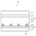
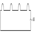
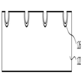
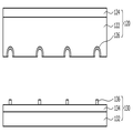
도 2 내지 도 9는 본 발명의 한 실시예에 따른 표시 장치의 제조 방법을 설명하기 위한 개략적인 단면도이다.
도 10은 본 발명의 다른 실시예에 따른 표시 장치의 개략적인 단면도이다.
도 11은 본 발명의 다른 실시예에 따른 표시 장치의 개략적인 단면도이다.
110, 210, 310: 표시 부재
120, 220, 320: 도광 부재
122, 222, 322: 도광층
123, 223: 도광층의 홈
124, 224, 324: 확산층
126, 226: 형광막
130, 230, 330: 광원 부재
132, 232: 회로 기판
134, 234, 327: 반사층
136, 236, 332: 광원 칩
150: 몰드 제작용 판
153: 몰드 제작용 판의 홈
160: 몰드
170: 롤
312, 314: 표시판
323: 접착층
325: 역프리즘층
334: 광원 지지 부재
Claims (15)
- 영상을 표시하는 표시 부재,
빛을 생성하는 광원 부재, 그리고
상기 광원 부재와 상기 표시 부재 사이에 위치하며 상기 빛을 상기 표시 부재로 안내하는 도광 부재
를 포함하고,
상기 표시 부재, 상기 광원 부재 및 상기 도광 부재는 일체로 형성되고,
상기 광원 부재는 청색 광을 생성하며,
상기 도광 부재는,
도광층, 그리고
상기 도광층의 윗면 또는 아랫면에 위치하며 상기 청색 광을 백색 광으로 변환하는 형광막
을 포함하는
표시 장치. - 제1항에서,
상기 도광층은 아랫 면에 형성되어 있으며 렌즈의 역할을 수행하는 복수의 홈을 가지는 표시 장치. - 제2항에서,
상기 도광 부재는 상기 도광층 위에 위치하는 확산층을 더 포함하는 표시 장치. - 제3항에서,
상기 형광막은 상기 홈의 표면에 도포되어 있는 표시 장치. - 제3항에서,
상기 형광막은 상기 확산층의 윗면에 위치하는 표시 장치. - 제5항에서,
상기 형광막은 양자점을 포함하는 표시 장치. - 제2항에서,
상기 광원 부재는 상기 홈 내에 위치하는 광원 칩을 포함하는 표시 장치. - 제7항에서,
상기 광원 부재는,
상기 광원 칩이 장착되어 있는 회로 기판, 그리고
상기 도광층 상부에 위치하는 반사층
을 더 포함하는
표시 장치. - 영상을 표시하는 표시 부재,
빛을 생성하며 상기 표시 부재의 가장자리에 부착되어 있는 광원 부재, 그리고
상기 표시 부재의 하부에 위치하며 상기 빛을 상기 표시 부재로 안내하는 도광 부재
를 포함하는 표시 장치. - 제9항에서,
상기 도광 부재는,
도광층,
상기 도광층의 윗면에 위치하는 확산층,
상기 도광층과 상기 확산층 사이에 위치하는 접착층, 그리고
상기 도광층의 하부에 위치하는 반사층
을 포함하는
표시 장치. - 제10항에서,
상기 도광 부재는 상기 확산층과 상기 접착층 사이에 위치하는 역프리즘층을 더 포함하는 표시 장치. - 제9항에서,
상기 표시 부재는 서로 결합되어 있는 제1 표시판과 제2 표시판을 포함하고,
상기 제1 표시판은 상기 제2 표시판보다 크며,
상기 광원 부재는 상기 제1 표시판에 부착되어 있는
표시 장치. - 서로 반대쪽에 위치한 제1면과 제2면을 가지는 도광층의 제1면에 복수의 홈을 형성하는 단계,
상기 홈에 형광막을 형성하는 단계,
상기 도광층의 제2면 위에 확산층을 적층하여 도광 부재를 형성하는 단계,
복수의 광원 칩을 포함하는 광원 부재를 상기 광원 칩이 상기 홈과 대응되도록 상기 도광 부재와 정렬시키는 단계,
상기 홈에 상기 광원 칩에 수용되도록 상기 도광 부재와 상기 광원 부재를 접착하는 단계, 그리고
상기 도광 부재에 표시 부재를 부착하는 단계
를 포함하는 표시 장치의 제조 방법. - 제13항에서,
상기 도광층의 제1면에 복수의 홈을 형성하는 단계는,
상기 도광층의 홈과 동일한 모양과 배치를 가지는 홈을 몰드 제작용 판에 형성하는 단계,
광경화성 수지를 상기 몰드 제작용 판에 도포하는 단계,
상기 광경화성 수지를 경화시켜 몰드를 형성하는 단계, 그리고
상기 몰드를 사용하여 상기 도광층에 홈을 형성하는 단계
를 포함하는
표시 장치의 제조 방법. - 제14항에서,
상기 몰드는 가요성 재질을 포함하며,
상기 몰드를 사용하여 상기 도광층에 홈을 형성하는 단계는 상기 몰드를 롤의 외주면에 부착하는 단계를 포함하는
표시 장치의 제조 방법.
Priority Applications (2)
| Application Number | Priority Date | Filing Date | Title |
|---|---|---|---|
| KR1020120158589A KR20140089014A (ko) | 2012-12-31 | 2012-12-31 | 표시 장치 및 그 제조 방법 |
| US13/911,556 US9297946B2 (en) | 2012-12-31 | 2013-06-06 | Display device and method of manufacturing the same |
Applications Claiming Priority (1)
| Application Number | Priority Date | Filing Date | Title |
|---|---|---|---|
| KR1020120158589A KR20140089014A (ko) | 2012-12-31 | 2012-12-31 | 표시 장치 및 그 제조 방법 |
Publications (1)
| Publication Number | Publication Date |
|---|---|
| KR20140089014A true KR20140089014A (ko) | 2014-07-14 |
Family
ID=51017014
Family Applications (1)
| Application Number | Title | Priority Date | Filing Date |
|---|---|---|---|
| KR1020120158589A Ceased KR20140089014A (ko) | 2012-12-31 | 2012-12-31 | 표시 장치 및 그 제조 방법 |
Country Status (2)
| Country | Link |
|---|---|
| US (1) | US9297946B2 (ko) |
| KR (1) | KR20140089014A (ko) |
Families Citing this family (23)
| Publication number | Priority date | Publication date | Assignee | Title |
|---|---|---|---|---|
| WO2015129222A1 (ja) | 2014-02-28 | 2015-09-03 | パナソニックIpマネジメント株式会社 | 発光素子および発光装置 |
| JP2016034017A (ja) | 2014-02-28 | 2016-03-10 | パナソニックIpマネジメント株式会社 | 発光装置 |
| WO2015129223A1 (ja) * | 2014-02-28 | 2015-09-03 | パナソニックIpマネジメント株式会社 | 発光装置 |
| EP3113237B1 (en) | 2014-02-28 | 2019-04-24 | Panasonic Intellectual Property Management Co., Ltd. | Light-emitting device |
| JP6380096B2 (ja) * | 2014-12-26 | 2018-08-29 | 日亜化学工業株式会社 | 発光装置 |
| RU2696671C2 (ru) | 2015-01-06 | 2019-08-05 | Филипс Лайтинг Холдинг Б.В. | Светоизлучающее устройство для светящихся поверхностей |
| US10182702B2 (en) | 2015-03-13 | 2019-01-22 | Panasonic Intellectual Property Management Co., Ltd. | Light-emitting apparatus including photoluminescent layer |
| US10031276B2 (en) | 2015-03-13 | 2018-07-24 | Panasonic Intellectual Property Management Co., Ltd. | Display apparatus including photoluminescent layer |
| JP6569856B2 (ja) | 2015-03-13 | 2019-09-04 | パナソニックIpマネジメント株式会社 | 発光装置および内視鏡 |
| JP2016171228A (ja) | 2015-03-13 | 2016-09-23 | パナソニックIpマネジメント株式会社 | 発光素子、発光装置および検知装置 |
| WO2016171109A1 (ja) * | 2015-04-20 | 2016-10-27 | シャープ株式会社 | 照明装置、表示装置、及びテレビ受信装置 |
| JP2017003697A (ja) | 2015-06-08 | 2017-01-05 | パナソニックIpマネジメント株式会社 | 発光素子および発光装置 |
| JP2017005054A (ja) | 2015-06-08 | 2017-01-05 | パナソニックIpマネジメント株式会社 | 発光装置 |
| JP6748905B2 (ja) | 2015-08-20 | 2020-09-02 | パナソニックIpマネジメント株式会社 | 発光装置 |
| US10359155B2 (en) | 2015-08-20 | 2019-07-23 | Panasonic Intellectual Property Management Co., Ltd. | Light-emitting apparatus |
| JP2017040818A (ja) | 2015-08-20 | 2017-02-23 | パナソニックIpマネジメント株式会社 | 発光素子 |
| JP6719094B2 (ja) | 2016-03-30 | 2020-07-08 | パナソニックIpマネジメント株式会社 | 発光素子 |
| CN107170772A (zh) * | 2017-05-23 | 2017-09-15 | 深圳市华星光电技术有限公司 | 微发光二极管阵列基板的封装结构 |
| CN110231734A (zh) * | 2018-03-06 | 2019-09-13 | 中强光电股份有限公司 | 光源模块及其面光源组件 |
| TWI666495B (zh) * | 2018-03-06 | 2019-07-21 | 友達光電股份有限公司 | 背光模組 |
| DE102018210546A1 (de) * | 2018-06-28 | 2020-01-02 | Osram Gmbh | Leuchtvorrichtung, scheinwerfer und verfahren |
| KR102639988B1 (ko) * | 2018-12-11 | 2024-02-22 | 엘지디스플레이 주식회사 | 표시장치 |
| US11681090B2 (en) | 2019-05-30 | 2023-06-20 | Nichia Corporation | Light emitting module and method of manufacturing same |
Family Cites Families (24)
| Publication number | Priority date | Publication date | Assignee | Title |
|---|---|---|---|---|
| KR19980060839A (ko) | 1996-12-31 | 1998-10-07 | 손욱 | 칼라 액정표시소자 |
| KR100615834B1 (ko) | 1999-08-03 | 2006-08-25 | 삼성전자주식회사 | 휘도를 향상시킨 액정표시장치 |
| JP2002042535A (ja) * | 2000-07-05 | 2002-02-08 | Internatl Business Mach Corp <Ibm> | 表示装置及び面上光源装置 |
| JP3906653B2 (ja) | 2000-07-18 | 2007-04-18 | ソニー株式会社 | 画像表示装置及びその製造方法 |
| JP4055405B2 (ja) | 2001-12-03 | 2008-03-05 | ソニー株式会社 | 電子部品及びその製造方法 |
| US7557781B2 (en) * | 2003-01-06 | 2009-07-07 | Tpo Displays Corp. | Planar display structure with LED light source |
| EP1455398A3 (en) * | 2003-03-03 | 2011-05-25 | Toyoda Gosei Co., Ltd. | Light emitting device comprising a phosphor layer and method of making same |
| TW200523503A (en) | 2003-09-29 | 2005-07-16 | Sony Corp | Backlight, light guiding plate, method for manufacturing diffusion plate and light guiding plate, and liquid crystal display device |
| KR101002343B1 (ko) | 2003-12-19 | 2010-12-17 | 엘지디스플레이 주식회사 | 액정표시장치의 제조방법 |
| KR20060012959A (ko) * | 2004-08-05 | 2006-02-09 | 삼성전자주식회사 | 표시 장치용 백라이트 |
| TWI274934B (en) * | 2004-09-23 | 2007-03-01 | Jemitek Electronics Corp | Flat display module |
| JP2006184872A (ja) | 2004-12-03 | 2006-07-13 | Sony Corp | 液晶表示装置 |
| KR20070010478A (ko) | 2005-07-19 | 2007-01-24 | 삼성전자주식회사 | 광학시트, 이를 갖는 백라이트 어셈블리 및 이를 갖는표시장치 |
| JP2007042901A (ja) * | 2005-08-04 | 2007-02-15 | Rohm Co Ltd | 発光モジュールおよび発光ユニット |
| CN101292178B (zh) * | 2005-10-17 | 2011-01-26 | 三菱丽阳株式会社 | 棱镜片及其制造方法以及面光源装置 |
| KR101255000B1 (ko) | 2006-06-21 | 2013-04-16 | 삼성디스플레이 주식회사 | 일체형 광학판, 이를 갖는 백라이트 어셈블리 및액정표시장치 |
| JP5104459B2 (ja) | 2008-03-27 | 2012-12-19 | 凸版印刷株式会社 | 光学部材とそれを用いたバックライト・ユニット、ディスプレイ |
| EP2326868A1 (en) | 2008-09-16 | 2011-06-01 | Koninklijke Philips Electronics N.V. | Colour mixing method for consistent colour quality |
| KR20100090914A (ko) | 2009-02-09 | 2010-08-18 | 삼성모바일디스플레이주식회사 | 도광필름 및 이를 구비한 백라이트 유닛 |
| KR20100106790A (ko) * | 2009-03-24 | 2010-10-04 | 삼성전자주식회사 | 표시 장치 |
| JP2010251360A (ja) | 2009-04-10 | 2010-11-04 | Sony Corp | 表示装置の製造方法および表示装置 |
| JP5382787B2 (ja) * | 2009-06-05 | 2014-01-08 | シチズン電子株式会社 | 面状光源及び液晶表示装置 |
| WO2011104972A1 (ja) * | 2010-02-25 | 2011-09-01 | シャープ株式会社 | 光源装置、表示装置 |
| JP5249283B2 (ja) * | 2010-05-10 | 2013-07-31 | デクセリアルズ株式会社 | 緑色発光蛍光体粒子及びその製造方法、並びに、色変換シート、発光装置及び画像表示装置組立体 |
-
2012
- 2012-12-31 KR KR1020120158589A patent/KR20140089014A/ko not_active Ceased
-
2013
- 2013-06-06 US US13/911,556 patent/US9297946B2/en active Active
Also Published As
| Publication number | Publication date |
|---|---|
| US9297946B2 (en) | 2016-03-29 |
| US20140185316A1 (en) | 2014-07-03 |
Similar Documents
| Publication | Publication Date | Title |
|---|---|---|
| KR20140089014A (ko) | 표시 장치 및 그 제조 방법 | |
| US8467013B2 (en) | Light guides | |
| JP5628918B2 (ja) | バックライトユニット及びディスプレイ装置 | |
| KR102131815B1 (ko) | 광원 어셈블리, 이를 포함하는 표시 장치 및 이의 제조 방법 | |
| TWI542910B (zh) | 光導元件及其製造方法以及顯示元件 | |
| CN104698828B (zh) | 智能手表和液晶屏 | |
| CN107438905B (zh) | 发光器件阵列及包含该发光器件阵列的照明系统 | |
| US11804580B2 (en) | Lighting device and method of producing light source substrate | |
| WO2015132943A1 (ja) | 表示装置 | |
| KR20050082994A (ko) | 발광 패널 어셈블리 | |
| KR20130039463A (ko) | 백라이트유니트용 복합시트 및 그 제조 방법 | |
| JP2007033597A (ja) | 光学シート、バックライトユニット、電気光学装置及び電子機器、並びに光学シートの製造方法及び光学シートの切断方法 | |
| TWI484262B (zh) | 控制光通量之元件、顯示裝置以及光發射裝置 | |
| CN108153030A (zh) | 一种3d显示装置 | |
| US10386561B2 (en) | Display device and method for manufacturing the same | |
| KR102045811B1 (ko) | 표시장치 | |
| JP2013068872A (ja) | レンズシート、及びel発光装置 | |
| KR102611355B1 (ko) | 양자점 시트와 이를 이용한 백라이트 유닛 및 디스플레이 장치 | |
| JP2010092777A (ja) | 面状ライトユニット及び表示装置 | |
| CN219978663U (zh) | 发光基板、背光模组和显示装置 | |
| KR101417258B1 (ko) | 광속 제어 부재 및 이를 포함하는 표시장치 | |
| KR101393796B1 (ko) | 광학 부재 및 이를 포함하는 표시 장치 | |
| KR101923501B1 (ko) | 마이크로렌즈 시트 및 마이크로렌즈 시트를 포함하는 백라이트 유닛 | |
| KR20140079592A (ko) | 백 라이트 유닛 및 이를 이용한 액정 표시장치와 그 제조 방법 | |
| KR101946840B1 (ko) | 광속 제어 부재, 발광 장치 및 표시장치 |
Legal Events
| Date | Code | Title | Description |
|---|---|---|---|
| PA0109 | Patent application |
Patent event code: PA01091R01D Comment text: Patent Application Patent event date: 20121231 |
|
| PG1501 | Laying open of application | ||
| A201 | Request for examination | ||
| PA0201 | Request for examination |
Patent event code: PA02012R01D Patent event date: 20171201 Comment text: Request for Examination of Application Patent event code: PA02011R01I Patent event date: 20121231 Comment text: Patent Application |
|
| E902 | Notification of reason for refusal | ||
| PE0902 | Notice of grounds for rejection |
Comment text: Notification of reason for refusal Patent event date: 20181218 Patent event code: PE09021S01D |
|
| AMND | Amendment | ||
| E601 | Decision to refuse application | ||
| PE0601 | Decision on rejection of patent |
Patent event date: 20190514 Comment text: Decision to Refuse Application Patent event code: PE06012S01D Patent event date: 20181218 Comment text: Notification of reason for refusal Patent event code: PE06011S01I |
|
| X091 | Application refused [patent] | ||
| AMND | Amendment | ||
| PX0901 | Re-examination |
Patent event code: PX09011S01I Patent event date: 20190514 Comment text: Decision to Refuse Application Patent event code: PX09012R01I Patent event date: 20190218 Comment text: Amendment to Specification, etc. |
|
| PX0601 | Decision of rejection after re-examination |
Comment text: Decision to Refuse Application Patent event code: PX06014S01D Patent event date: 20190701 Comment text: Amendment to Specification, etc. Patent event code: PX06012R01I Patent event date: 20190614 Comment text: Decision to Refuse Application Patent event code: PX06011S01I Patent event date: 20190514 Comment text: Amendment to Specification, etc. Patent event code: PX06012R01I Patent event date: 20190218 Comment text: Notification of reason for refusal Patent event code: PX06013S01I Patent event date: 20181218 |
|
| X601 | Decision of rejection after re-examination |