KR20140096341A - Cvd 반응기 및 cvd 반응기용 기판 홀더 - Google Patents
Cvd 반응기 및 cvd 반응기용 기판 홀더 Download PDFInfo
- Publication number
- KR20140096341A KR20140096341A KR1020147015105A KR20147015105A KR20140096341A KR 20140096341 A KR20140096341 A KR 20140096341A KR 1020147015105 A KR1020147015105 A KR 1020147015105A KR 20147015105 A KR20147015105 A KR 20147015105A KR 20140096341 A KR20140096341 A KR 20140096341A
- Authority
- KR
- South Korea
- Prior art keywords
- substrate holder
- substrate
- heating system
- gap
- Prior art date
- Legal status (The legal status is an assumption and is not a legal conclusion. Google has not performed a legal analysis and makes no representation as to the accuracy of the status listed.)
- Granted
Links
Images





Classifications
-
- C—CHEMISTRY; METALLURGY
- C23—COATING METALLIC MATERIAL; COATING MATERIAL WITH METALLIC MATERIAL; CHEMICAL SURFACE TREATMENT; DIFFUSION TREATMENT OF METALLIC MATERIAL; COATING BY VACUUM EVAPORATION, BY SPUTTERING, BY ION IMPLANTATION OR BY CHEMICAL VAPOUR DEPOSITION, IN GENERAL; INHIBITING CORROSION OF METALLIC MATERIAL OR INCRUSTATION IN GENERAL
- C23C—COATING METALLIC MATERIAL; COATING MATERIAL WITH METALLIC MATERIAL; SURFACE TREATMENT OF METALLIC MATERIAL BY DIFFUSION INTO THE SURFACE, BY CHEMICAL CONVERSION OR SUBSTITUTION; COATING BY VACUUM EVAPORATION, BY SPUTTERING, BY ION IMPLANTATION OR BY CHEMICAL VAPOUR DEPOSITION, IN GENERAL
- C23C16/00—Chemical coating by decomposition of gaseous compounds, without leaving reaction products of surface material in the coating, i.e. chemical vapour deposition [CVD] processes
- C23C16/44—Chemical coating by decomposition of gaseous compounds, without leaving reaction products of surface material in the coating, i.e. chemical vapour deposition [CVD] processes characterised by the method of coating
- C23C16/458—Chemical coating by decomposition of gaseous compounds, without leaving reaction products of surface material in the coating, i.e. chemical vapour deposition [CVD] processes characterised by the method of coating characterised by the method used for supporting substrates in the reaction chamber
-
- C—CHEMISTRY; METALLURGY
- C23—COATING METALLIC MATERIAL; COATING MATERIAL WITH METALLIC MATERIAL; CHEMICAL SURFACE TREATMENT; DIFFUSION TREATMENT OF METALLIC MATERIAL; COATING BY VACUUM EVAPORATION, BY SPUTTERING, BY ION IMPLANTATION OR BY CHEMICAL VAPOUR DEPOSITION, IN GENERAL; INHIBITING CORROSION OF METALLIC MATERIAL OR INCRUSTATION IN GENERAL
- C23C—COATING METALLIC MATERIAL; COATING MATERIAL WITH METALLIC MATERIAL; SURFACE TREATMENT OF METALLIC MATERIAL BY DIFFUSION INTO THE SURFACE, BY CHEMICAL CONVERSION OR SUBSTITUTION; COATING BY VACUUM EVAPORATION, BY SPUTTERING, BY ION IMPLANTATION OR BY CHEMICAL VAPOUR DEPOSITION, IN GENERAL
- C23C16/00—Chemical coating by decomposition of gaseous compounds, without leaving reaction products of surface material in the coating, i.e. chemical vapour deposition [CVD] processes
- C23C16/44—Chemical coating by decomposition of gaseous compounds, without leaving reaction products of surface material in the coating, i.e. chemical vapour deposition [CVD] processes characterised by the method of coating
- C23C16/455—Chemical coating by decomposition of gaseous compounds, without leaving reaction products of surface material in the coating, i.e. chemical vapour deposition [CVD] processes characterised by the method of coating characterised by the method used for introducing gases into reaction chamber or for modifying gas flows in reaction chamber
-
- C—CHEMISTRY; METALLURGY
- C23—COATING METALLIC MATERIAL; COATING MATERIAL WITH METALLIC MATERIAL; CHEMICAL SURFACE TREATMENT; DIFFUSION TREATMENT OF METALLIC MATERIAL; COATING BY VACUUM EVAPORATION, BY SPUTTERING, BY ION IMPLANTATION OR BY CHEMICAL VAPOUR DEPOSITION, IN GENERAL; INHIBITING CORROSION OF METALLIC MATERIAL OR INCRUSTATION IN GENERAL
- C23C—COATING METALLIC MATERIAL; COATING MATERIAL WITH METALLIC MATERIAL; SURFACE TREATMENT OF METALLIC MATERIAL BY DIFFUSION INTO THE SURFACE, BY CHEMICAL CONVERSION OR SUBSTITUTION; COATING BY VACUUM EVAPORATION, BY SPUTTERING, BY ION IMPLANTATION OR BY CHEMICAL VAPOUR DEPOSITION, IN GENERAL
- C23C16/00—Chemical coating by decomposition of gaseous compounds, without leaving reaction products of surface material in the coating, i.e. chemical vapour deposition [CVD] processes
- C23C16/44—Chemical coating by decomposition of gaseous compounds, without leaving reaction products of surface material in the coating, i.e. chemical vapour deposition [CVD] processes characterised by the method of coating
- C23C16/46—Chemical coating by decomposition of gaseous compounds, without leaving reaction products of surface material in the coating, i.e. chemical vapour deposition [CVD] processes characterised by the method of coating characterised by the method used for heating the substrate
-
- H—ELECTRICITY
- H10—SEMICONDUCTOR DEVICES; ELECTRIC SOLID-STATE DEVICES NOT OTHERWISE PROVIDED FOR
- H10P—GENERIC PROCESSES OR APPARATUS FOR THE MANUFACTURE OR TREATMENT OF DEVICES COVERED BY CLASS H10
- H10P72/00—Handling or holding of wafers, substrates or devices during manufacture or treatment thereof
- H10P72/04—Apparatus for manufacture or treatment
- H10P72/0431—Apparatus for thermal treatment
- H10P72/0434—Apparatus for thermal treatment mainly by convection
-
- H—ELECTRICITY
- H10—SEMICONDUCTOR DEVICES; ELECTRIC SOLID-STATE DEVICES NOT OTHERWISE PROVIDED FOR
- H10P—GENERIC PROCESSES OR APPARATUS FOR THE MANUFACTURE OR TREATMENT OF DEVICES COVERED BY CLASS H10
- H10P72/00—Handling or holding of wafers, substrates or devices during manufacture or treatment thereof
- H10P72/70—Handling or holding of wafers, substrates or devices during manufacture or treatment thereof for supporting or gripping
- H10P72/76—Handling or holding of wafers, substrates or devices during manufacture or treatment thereof for supporting or gripping using mechanical means, e.g. clamps or pinches
- H10P72/7604—Handling or holding of wafers, substrates or devices during manufacture or treatment thereof for supporting or gripping using mechanical means, e.g. clamps or pinches the wafers being placed on a susceptor, stage or support
- H10P72/7611—Handling or holding of wafers, substrates or devices during manufacture or treatment thereof for supporting or gripping using mechanical means, e.g. clamps or pinches the wafers being placed on a susceptor, stage or support characterised by edge profile or support profile
-
- H—ELECTRICITY
- H10—SEMICONDUCTOR DEVICES; ELECTRIC SOLID-STATE DEVICES NOT OTHERWISE PROVIDED FOR
- H10P—GENERIC PROCESSES OR APPARATUS FOR THE MANUFACTURE OR TREATMENT OF DEVICES COVERED BY CLASS H10
- H10P72/00—Handling or holding of wafers, substrates or devices during manufacture or treatment thereof
- H10P72/70—Handling or holding of wafers, substrates or devices during manufacture or treatment thereof for supporting or gripping
- H10P72/76—Handling or holding of wafers, substrates or devices during manufacture or treatment thereof for supporting or gripping using mechanical means, e.g. clamps or pinches
- H10P72/7604—Handling or holding of wafers, substrates or devices during manufacture or treatment thereof for supporting or gripping using mechanical means, e.g. clamps or pinches the wafers being placed on a susceptor, stage or support
- H10P72/7614—Handling or holding of wafers, substrates or devices during manufacture or treatment thereof for supporting or gripping using mechanical means, e.g. clamps or pinches the wafers being placed on a susceptor, stage or support characterised by a plurality of individual support members, e.g. support posts or protrusions
-
- H—ELECTRICITY
- H10—SEMICONDUCTOR DEVICES; ELECTRIC SOLID-STATE DEVICES NOT OTHERWISE PROVIDED FOR
- H10P—GENERIC PROCESSES OR APPARATUS FOR THE MANUFACTURE OR TREATMENT OF DEVICES COVERED BY CLASS H10
- H10P72/00—Handling or holding of wafers, substrates or devices during manufacture or treatment thereof
- H10P72/70—Handling or holding of wafers, substrates or devices during manufacture or treatment thereof for supporting or gripping
- H10P72/76—Handling or holding of wafers, substrates or devices during manufacture or treatment thereof for supporting or gripping using mechanical means, e.g. clamps or pinches
- H10P72/7604—Handling or holding of wafers, substrates or devices during manufacture or treatment thereof for supporting or gripping using mechanical means, e.g. clamps or pinches the wafers being placed on a susceptor, stage or support
- H10P72/7621—Handling or holding of wafers, substrates or devices during manufacture or treatment thereof for supporting or gripping using mechanical means, e.g. clamps or pinches the wafers being placed on a susceptor, stage or support characterised by supporting two or more semiconductor substrates
Landscapes
- Chemical & Material Sciences (AREA)
- General Chemical & Material Sciences (AREA)
- Chemical Kinetics & Catalysis (AREA)
- Engineering & Computer Science (AREA)
- Materials Engineering (AREA)
- Mechanical Engineering (AREA)
- Metallurgy (AREA)
- Organic Chemistry (AREA)
- Chemical Vapour Deposition (AREA)
Abstract
Description
도 2는 도 1의 라인 Ⅱ-Ⅱ에 따라 절단한 단면도이며;
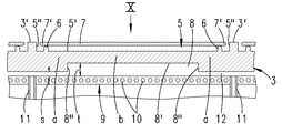
도 3은 하나의 개별적인 포켓 영역을 확대하여 도시한 도 2에 따른 도면이고;
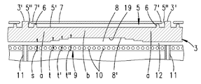
도 4는 아래로 만곡된 기판(7)을 갖는 도 3에 따른 도면이며;
도 5는 위로 만곡된 기판(7)을 갖는 도 3에 따른 제 2 실시예이고;
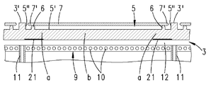
도 6은 도 3에 따른 도면으로 도시한 본 발명의 제 3 실시예이며;
도 7은 도 3에 따른 제 4 실시예이고;
도 8은 도 3에 따른 제 5 실시예이며;
도 9는 도 3에 따른 제 6 실시예이고; 그리고
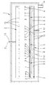
도 10은 하나의 개별적인 포켓을 평면도로 도시한 도면이다.
2 가스 유입 부재
3 기판 홀더
3' 기판 홀더 상부면
3" 기판 홀더 하부면
4 공정 챔버
5 포켓
5' 포켓 바닥
5" 포켓 에지
6 지지부, 리브
6' 단부
7 기판
7' 기판 홀더 에지
8 리세스
8' 바닥
8" 포켓 벽
9 가열 시스템
10 가열 코일
11 플러싱 가스 유입구
12 간극
13 가스 공급 라인
14 가스 배출 라인
15 가스 유출 개구
16 중단부
17 돌출부
18 리세스, 볼 모양
19 리세스
20 반사 작용하는 표면
21 반사 작용하는 표면
a 주변부
b 중심부
s 간극 높이
t 간극 높이
Claims (13)
- CVD 반응기로서,
반응기 하우징(1), 공정 챔버(4), 기판 홀더(3) 및 가열 시스템(9)을 구비하며, 상기 반응기 하우징(1) 내에 배치된 공정 챔버(4) 내부로는 가스 유입 부재(gas inlet member)(2)에 의해 하나 이상의 공정 가스가 공급될 수 있고, 상기 공정 챔버(4) 쪽을 향하는 상기 기판 홀더(3)의 상부면(3')은, 각각의 기판(7)이 단지 선택된 그리고 포켓(5)의 바닥(5')에 비해 상승된 지지부(6)들 상에서만 지지되도록 형성된 하나 또는 다수의 포켓(pocket)(5)을 가지며, 그리고 상기 기판 홀더(3) 아래에 배치된 가열 시스템(9)은 간극(12)으로 인해 상기 기판 홀더(3)의 하부면(3")으로부터 이격되어 배치되어 있으며, 이 경우 상기 가열 시스템(9)으로부터 기판 홀더(3)로의 열전달과 관련하여, 상기 포켓(5)의 중앙 구역에 위치한 중심부(b)에서는 상기 기판 홀더(3)의 하부면(3")이 상기 중심부(b)를 둘러싸는 그리고 상기 포켓(5)의 에지 인접 구역 아래에 위치한 주변부(a)에서와 다르게 형성되어 있고,
상기 가열 시스템(9)이 대체로 평면형 열원(heat source)으로서 형성되어 있고, 열전도율이 상이한 플러싱 가스(flushing gas)들을 이용해 상기 간극(12)을 세척하기 위해 가스 플러싱 장치(gas flushing device)(11)가 제공되어 있으며, 그리고 상기 간극(12)은, 제 1 열전도율을 갖는 제 1 플러싱 가스를 제 2 열전도율을 갖는 제 2 플러싱 가스로 교체 시 상기 주변부(a)에서, 상기 가열 시스템(9)으로부터 기판 홀더(3)로의 열공급이 상기 중심부(b)에서와 다르게 변경되도록 하는 간극 높이(s, t)를 가지는,
CDV 반응기. - 제 1항에 있어서,
상기 중심부(b)에서 상기 간극(12)의 간극 높이(t, t', t")가 상기 주변부(a)에서 간극 높이(s)와 다른,
CVD 반응기. - 제 1항 또는 제 2항에 있어서,
상기 기판 홀더(3)의 하부면(3")이 상기 중심부(b)에서 리세스(8)를 가지는,
CVD 반응기. - 제 1항 내지 제 3항 중 어느 한 항 또는 다수의 항에 있어서,
상기 포켓(5) 또는 리세스(8)의 바닥(5', 8')이 예를 들면 볼 모양으로(bowl-shaped) 만곡된,
CDV 반응기. - 제 1항 내지 제 4항 중 어느 한 항 또는 다수의 항에 있어서,
상기 바닥(5', 8')의 만곡부가 계단 형상과 유사하게 형성된,
CVD 반응기. - 제 1항 내지 제 5항 중 어느 한 항 또는 다수의 항에 있어서,
상기 중심부(b)에서 상기 기판 홀더(3)의 하부면(3")이 상기 주변부(a) 둘레와 다른 반사율을 가지는,
CVD 반응기. - 제 1항 내지 제 6항 중 어느 한 항 또는 다수의 항에 있어서,
상기 중심부(b) 및/또는 주변부(a)가 반사 작용하는 코팅으로 코팅된,
CVD 반응기. - 제 1항 내지 제 7항 중 어느 한 항 또는 다수의 항에 있어서,
상기 가열 시스템(9)이 나선형으로 배치된 열선(heating wire)(10)에 의해 형성된,
CVD 반응기. - 각각의 공정 단계에서, 특히 제 1항 내지 제 8항 중 어느 한 항 또는 다수의 항에 따른 CVD 반응기의 기판(7) 상에 겹쳐서 배치되는 다수의 층을 증착하기 위한 방법으로서,
이 경우 적어도 하나의 제 1 공정 단계에서는 제 1 조성물을 갖는 제 1 층이 제 1 온도에서 증착되고, 적어도 하나의 제 2 공정 단계에서는 제 2 조성물을 갖는 제 2 층이 제 2 온도에서 증착되며, 이 경우 상기 제 1 및 제 2 조성물 그리고 상기 제 1 및 제 2 온도가 서로 상이하고,
상기 제 1 공정 단계에서는 제 1 플러싱 가스 또는 플러싱 가스 혼합물이 간극(12) 내로 공급되고, 상기 제 2 공정 단계에서는 제 2 플러싱 가스 또는 플러싱 가스 혼합물이 상기 간극(12) 내로 공급되며, 이 경우 적어도 그들이 갖는 열전도율로 인해 상기 제 1 플러싱 가스 또는 플러싱 가스 혼합물과 상기 제 2 플러싱 가스 또는 플러싱 가스 혼합물이 구별되는,
층을 증착하기 위한 방법. - 제 9항에 있어서,
상기 제 1 공정 단계에서, 가열 시스템(9)으로부터 기판 홀더(3)로 열전달 시 주변부(b)와 중심부(a) 중 하나 이상의 영역에서 열복사가 우세하고, 상기 제 2 공정 단계에서는 열전도가 우세한,
층을 증착하기 위한 방법. - 제 9항 또는 제 10항에 있어서,
상기 제 1 공정 단계에서, 포켓(5) 바닥(5')의 중앙 구역의 평균 온도가 상기 포켓 바닥(5')의 에지부의 평균 온도에 대략 일치하고, 상기 제 2 공정 단계에서는 두 평균 온도가 서로 상이한,
층을 증착하기 위한 방법. - 하나 또는 다수의 포켓(5)을 구비하는 기판 홀더로서,
상기 하나 또는 다수의 포켓(5)이 자체 에지(5")를 따라 뻗은 리브(rib)(6)로서 형성된 그리고 포켓(5)의 바닥(5')에 비해 상승된, 기판(7)용 지지부를 가지며, 그리고 상기 기판(7)의 에지(7')와 상기 포켓(5)의 에지(5")의 이격 상태를 유지하기 위해 상기 포켓 에지(5")로부터 다수의 돌출부(17)가 상기 포켓(5) 내부로 돌출하고,
상기 리브(6)가 돌출부(17)들의 영역에서 중단된,
기판 홀더. - 제 12항에 있어서,
중단부(16)들의 원주 길이가 상기 돌출부(17)들의 원주 길이와 대략 일치하는,
기판 홀더.
Applications Claiming Priority (3)
| Application Number | Priority Date | Filing Date | Title |
|---|---|---|---|
| DE102011055061.5 | 2011-11-04 | ||
| DE102011055061A DE102011055061A1 (de) | 2011-11-04 | 2011-11-04 | CVD-Reaktor bzw. Substrathalter für einen CVD-Reaktor |
| PCT/EP2012/071687 WO2013064613A2 (de) | 2011-11-04 | 2012-11-02 | Cvd-reaktor bzw. substrathalter für einen cvd-reaktor |
Publications (2)
| Publication Number | Publication Date |
|---|---|
| KR20140096341A true KR20140096341A (ko) | 2014-08-05 |
| KR102099216B1 KR102099216B1 (ko) | 2020-04-10 |
Family
ID=47178621
Family Applications (1)
| Application Number | Title | Priority Date | Filing Date |
|---|---|---|---|
| KR1020147015105A Active KR102099216B1 (ko) | 2011-11-04 | 2012-11-02 | Cvd 반응기 및 cvd 반응기용 기판 홀더 |
Country Status (6)
| Country | Link |
|---|---|
| US (2) | US20140287142A1 (ko) |
| KR (1) | KR102099216B1 (ko) |
| CN (1) | CN104053816B (ko) |
| DE (1) | DE102011055061A1 (ko) |
| TW (1) | TWI573895B (ko) |
| WO (1) | WO2013064613A2 (ko) |
Cited By (2)
| Publication number | Priority date | Publication date | Assignee | Title |
|---|---|---|---|---|
| KR20170088419A (ko) * | 2014-11-28 | 2017-08-01 | 아익스트론 에스이 | 기판 유지 장치 |
| KR20190129917A (ko) * | 2017-03-20 | 2019-11-20 | 아익스트론 에스이 | Cvd-반응기의 서셉터 |
Families Citing this family (38)
| Publication number | Priority date | Publication date | Assignee | Title |
|---|---|---|---|---|
| TWI397113B (zh) * | 2008-08-29 | 2013-05-21 | 維克儀器公司 | 具有可變熱阻之晶圓載體 |
| DE102011055061A1 (de) * | 2011-11-04 | 2013-05-08 | Aixtron Se | CVD-Reaktor bzw. Substrathalter für einen CVD-Reaktor |
| US10316412B2 (en) | 2012-04-18 | 2019-06-11 | Veeco Instruments Inc. | Wafter carrier for chemical vapor deposition systems |
| DE102012108986A1 (de) | 2012-09-24 | 2014-03-27 | Aixtron Se | Substrathalter einer CVD-Vorrichtung |
| US10167571B2 (en) | 2013-03-15 | 2019-01-01 | Veeco Instruments Inc. | Wafer carrier having provisions for improving heating uniformity in chemical vapor deposition systems |
| DE102013105896A1 (de) | 2013-06-07 | 2014-12-11 | Aixtron Se | Fertigungseinrichtung mit einem Magnetschienentransportsystem |
| DE102014100024A1 (de) * | 2014-01-02 | 2015-07-02 | Aixtron Se | Vorrichtung zur Anordnung von Substraten, insbesondere Suszeptor eines CVD-Reaktors |
| DE102014104218A1 (de) * | 2014-03-26 | 2015-10-01 | Aixtron Se | CVD-Reaktor mit Vorlaufzonen-Temperaturregelung |
| US20150292815A1 (en) * | 2014-04-10 | 2015-10-15 | Applied Materials, Inc. | Susceptor with radiation source compensation |
| DE102014114947A1 (de) | 2014-05-16 | 2015-11-19 | Aixtron Se | Vorrichtung zum Abscheiden von Halbleiterschichten sowie einen Suszeptor zur Verwendung in einer derartigen Vorrichtung |
| DE102014109327A1 (de) | 2014-07-03 | 2016-01-07 | Aixtron Se | Beschichtetes flaches scheibenförmiges Bauteil in einem CVD-Reaktor |
| US9748113B2 (en) | 2015-07-30 | 2017-08-29 | Veeco Intruments Inc. | Method and apparatus for controlled dopant incorporation and activation in a chemical vapor deposition system |
| DE102015113956B4 (de) * | 2015-08-24 | 2024-03-07 | Meyer Burger (Germany) Gmbh | Substratträger |
| JP6707827B2 (ja) * | 2015-09-28 | 2020-06-10 | 東京エレクトロン株式会社 | 成膜装置 |
| US10161041B2 (en) | 2015-10-14 | 2018-12-25 | Taiwan Semiconductor Manufacturing Co., Ltd. | Thermal chemical vapor deposition system and operating method thereof |
| CN105369220B (zh) * | 2015-12-14 | 2018-06-19 | 华中科技大学 | 一种用于气相沉积薄膜的装置 |
| DE102016103530A1 (de) | 2016-02-29 | 2017-08-31 | Aixtron Se | Substrathaltevorrichtung mit aus einer Ringnut entspringenden Tragvorsprüngen |
| US20180148835A1 (en) * | 2016-11-29 | 2018-05-31 | Lam Research Corporation | Substrate support with varying depths of areas between mesas and corresponding temperature dependent method of fabricating |
| KR102369676B1 (ko) | 2017-04-10 | 2022-03-04 | 삼성디스플레이 주식회사 | 표시 장치의 제조장치 및 표시 장치의 제조방법 |
| JP7018744B2 (ja) * | 2017-11-24 | 2022-02-14 | 昭和電工株式会社 | SiCエピタキシャル成長装置 |
| JP7495882B2 (ja) | 2018-04-13 | 2024-06-05 | ビーコ・インストゥルメンツ・インコーポレイテッド | マルチゾーンインジェクターブロックを備える化学蒸着装置 |
| JP7321768B2 (ja) * | 2018-05-23 | 2023-08-07 | 信越化学工業株式会社 | 化学気相成長装置および被膜形成方法 |
| US20210375663A1 (en) * | 2018-10-04 | 2021-12-02 | Toyo Tanso Co., Ltd. | Susceptor |
| DE102018131987A1 (de) * | 2018-12-12 | 2020-06-18 | Aixtron Se | Substrathalter zur Verwendung in einem CVD-Reaktor |
| DE102018132673A1 (de) * | 2018-12-18 | 2020-06-18 | Aixtron Se | Suszeptor für einen CVD-Reaktor |
| DE102019104433A1 (de) | 2019-02-21 | 2020-08-27 | Aixtron Se | CVD-Reaktor mit Mitteln zur lokalen Beeinflussung der Suszeptortemperatur |
| TWI711717B (zh) * | 2019-11-06 | 2020-12-01 | 錼創顯示科技股份有限公司 | 加熱裝置及化學氣相沉積系統 |
| TWI727907B (zh) * | 2019-11-06 | 2021-05-11 | 錼創顯示科技股份有限公司 | 加熱裝置及化學氣相沉積系統 |
| US11542604B2 (en) | 2019-11-06 | 2023-01-03 | PlayNitride Display Co., Ltd. | Heating apparatus and chemical vapor deposition system |
| DE102020105753A1 (de) | 2020-03-04 | 2021-09-09 | Aixtron Se | Auf einer Unterseite mit einer Vielzahl von Strukturelementen versehener Substrathalter für einen CVD-Reaktor |
| DE102020107517A1 (de) | 2020-03-18 | 2021-09-23 | Aixtron Se | Suszeptor für einen CVD-Reaktor |
| KR102405332B1 (ko) | 2020-05-07 | 2022-06-02 | 한국세라믹기술원 | 수직형 화학 증착기 |
| DE102020120449A1 (de) | 2020-08-03 | 2022-02-03 | OSRAM Opto Semiconductors Gesellschaft mit beschränkter Haftung | Wafer-carrier und system für eine epitaxievorrichtung |
| US20220076988A1 (en) * | 2020-09-10 | 2022-03-10 | Applied Materials, Inc. | Back side design for flat silicon carbide susceptor |
| DE102021003326B3 (de) * | 2021-06-28 | 2022-09-08 | Singulus Technologies Aktiengesellschaft | Substratträger |
| CN116072584A (zh) * | 2021-11-03 | 2023-05-05 | 中微半导体设备(上海)股份有限公司 | 多区控温的静电吸盘及等离子体处理装置 |
| DE102022101721A1 (de) | 2022-01-25 | 2023-07-27 | Meyer Burger (Germany) Gmbh | PECVD Beschichtungsverfahren |
| TW202542359A (zh) * | 2024-01-18 | 2025-11-01 | 美商蘭姆研究公司 | 用於在處理工具中加熱基板的熱調諧器 |
Citations (4)
| Publication number | Priority date | Publication date | Assignee | Title |
|---|---|---|---|---|
| US3892940A (en) * | 1972-07-01 | 1975-07-01 | Philips Corp | Apparatus for uniformly heating monocrystalline wafers |
| JP2002146540A (ja) * | 2000-11-14 | 2002-05-22 | Ebara Corp | 基板加熱装置 |
| US20040011286A1 (en) * | 2002-07-19 | 2004-01-22 | Hynix Semiconductor Inc. | Batch type atomic layer deposition apparatus and in-situ cleaning method thereof |
| US20060191483A1 (en) * | 2004-04-01 | 2006-08-31 | Blomiley Eric R | Substrate susceptor for receiving a substrate to be deposited upon |
Family Cites Families (39)
| Publication number | Priority date | Publication date | Assignee | Title |
|---|---|---|---|---|
| US4512841A (en) | 1984-04-02 | 1985-04-23 | International Business Machines Corporation | RF Coupling techniques |
| JPH01256118A (ja) * | 1988-04-05 | 1989-10-12 | Sumitomo Metal Ind Ltd | 気相反応装置 |
| JPH05166757A (ja) * | 1991-12-13 | 1993-07-02 | Tokyo Electron Ltd | 被処理体の温調装置 |
| US5226383A (en) * | 1992-03-12 | 1993-07-13 | Bell Communications Research, Inc. | Gas foil rotating substrate holder |
| JPH0610140A (ja) * | 1992-06-24 | 1994-01-18 | Fuji Film Micro Device Kk | 薄膜堆積装置 |
| US5645646A (en) * | 1994-02-25 | 1997-07-08 | Applied Materials, Inc. | Susceptor for deposition apparatus |
| FI97730C (fi) * | 1994-11-28 | 1997-02-10 | Mikrokemia Oy | Laitteisto ohutkalvojen valmistamiseksi |
| US6616767B2 (en) * | 1997-02-12 | 2003-09-09 | Applied Materials, Inc. | High temperature ceramic heater assembly with RF capability |
| US6432479B2 (en) * | 1997-12-02 | 2002-08-13 | Applied Materials, Inc. | Method for in-situ, post deposition surface passivation of a chemical vapor deposited film |
| JP2001168086A (ja) * | 1999-12-09 | 2001-06-22 | Kawasaki Steel Corp | 半導体装置の製造方法および製造装置 |
| DE10056029A1 (de) * | 2000-11-11 | 2002-05-16 | Aixtron Ag | Verfahren und Vorrichtung zur Temperatursteuerung der Oberflächentemperaturen von Substraten in einem CVD-Reaktor |
| US6755150B2 (en) * | 2001-04-20 | 2004-06-29 | Applied Materials Inc. | Multi-core transformer plasma source |
| US20030010775A1 (en) * | 2001-06-21 | 2003-01-16 | Hyoung June Kim | Methods and apparatuses for heat treatment of semiconductor films upon thermally susceptible non-conducting substrates |
| DE10133914A1 (de) * | 2001-07-12 | 2003-01-23 | Aixtron Ag | Prozesskammer mit abschnittsweise unterschiedlich drehangetriebenem Boden und Schichtabscheideverfahren in einer derartigen Prozesskammer |
| US20030089457A1 (en) * | 2001-11-13 | 2003-05-15 | Applied Materials, Inc. | Apparatus for controlling a thermal conductivity profile for a pedestal in a semiconductor wafer processing chamber |
| EP1451387A1 (en) * | 2001-12-04 | 2004-09-01 | Primaxx, Inc. | Chemical vapor deposition reactor |
| WO2005013334A2 (en) * | 2003-08-01 | 2005-02-10 | Sgl Carbon Ag | Holder for supporting wafers during semiconductor manufacture |
| JP4441356B2 (ja) * | 2003-10-16 | 2010-03-31 | 東京エレクトロン株式会社 | 成膜装置 |
| EP1699121B1 (en) * | 2003-12-15 | 2014-04-30 | The Furukawa Electric Co., Ltd. | Semiconductor device manufacturing method |
| US7585371B2 (en) * | 2004-04-08 | 2009-09-08 | Micron Technology, Inc. | Substrate susceptors for receiving semiconductor substrates to be deposited upon |
| DE202004013741U1 (de) | 2004-09-01 | 2004-11-04 | Sennheiser Electronic Gmbh & Co. Kg | Mikrofonhalter |
| DE102005055252A1 (de) * | 2005-11-19 | 2007-05-24 | Aixtron Ag | CVD-Reaktor mit gleitgelagerten Suszeptorhalter |
| DE102005056320A1 (de) * | 2005-11-25 | 2007-06-06 | Aixtron Ag | CVD-Reaktor mit einem Gaseinlassorgan |
| US8603248B2 (en) * | 2006-02-10 | 2013-12-10 | Veeco Instruments Inc. | System and method for varying wafer surface temperature via wafer-carrier temperature offset |
| JP4827569B2 (ja) * | 2006-03-23 | 2011-11-30 | 大日本スクリーン製造株式会社 | 基板支持構造とこれを用いた熱処理装置と基板支持構造に用いられるシート状物と基板支持構造の製造方法 |
| DE102006018514A1 (de) | 2006-04-21 | 2007-10-25 | Aixtron Ag | Vorrichtung und Verfahren zur Steuerung der Oberflächentemperatur eines Substrates in einer Prozesskammer |
| KR100867191B1 (ko) * | 2006-11-02 | 2008-11-06 | 주식회사 유진테크 | 기판처리장치 및 기판처리방법 |
| CN102174693B (zh) * | 2007-01-12 | 2014-10-29 | 威科仪器有限公司 | 气体处理系统 |
| US20080314319A1 (en) * | 2007-06-19 | 2008-12-25 | Memc Electronic Materials, Inc. | Susceptor for improving throughput and reducing wafer damage |
| TWI397113B (zh) * | 2008-08-29 | 2013-05-21 | 維克儀器公司 | 具有可變熱阻之晶圓載體 |
| JP4709945B2 (ja) * | 2009-04-13 | 2011-06-29 | パナソニック株式会社 | プラズマ処理装置及びプラズマ処理方法 |
| US20110049779A1 (en) * | 2009-08-28 | 2011-03-03 | Applied Materials, Inc. | Substrate carrier design for improved photoluminescence uniformity |
| DE102009043960A1 (de) * | 2009-09-08 | 2011-03-10 | Aixtron Ag | CVD-Reaktor |
| DE102009044276A1 (de) * | 2009-10-16 | 2011-05-05 | Aixtron Ag | CVD-Reaktor mit auf einem mehrere Zonen aufweisenden Gaspolster liegenden Substrathalter |
| KR100990746B1 (ko) * | 2009-11-19 | 2010-11-02 | (주)앤피에스 | 기판 처리 장치 |
| US20110259879A1 (en) * | 2010-04-22 | 2011-10-27 | Applied Materials, Inc. | Multi-Zone Induction Heating for Improved Temperature Uniformity in MOCVD and HVPE Chambers |
| US20120309115A1 (en) * | 2011-06-02 | 2012-12-06 | Applied Materials, Inc. | Apparatus and methods for supporting and controlling a substrate |
| DE102011055061A1 (de) * | 2011-11-04 | 2013-05-08 | Aixtron Se | CVD-Reaktor bzw. Substrathalter für einen CVD-Reaktor |
| US10932323B2 (en) * | 2015-08-03 | 2021-02-23 | Alta Devices, Inc. | Reflector and susceptor assembly for chemical vapor deposition reactor |
-
2011
- 2011-11-04 DE DE102011055061A patent/DE102011055061A1/de active Pending
-
2012
- 2012-11-02 CN CN201280064947.8A patent/CN104053816B/zh active Active
- 2012-11-02 TW TW101140700A patent/TWI573895B/zh active
- 2012-11-02 KR KR1020147015105A patent/KR102099216B1/ko active Active
- 2012-11-02 WO PCT/EP2012/071687 patent/WO2013064613A2/de not_active Ceased
- 2012-11-02 US US14/356,104 patent/US20140287142A1/en not_active Abandoned
-
2018
- 2018-04-03 US US15/944,677 patent/US10526705B2/en active Active
Patent Citations (4)
| Publication number | Priority date | Publication date | Assignee | Title |
|---|---|---|---|---|
| US3892940A (en) * | 1972-07-01 | 1975-07-01 | Philips Corp | Apparatus for uniformly heating monocrystalline wafers |
| JP2002146540A (ja) * | 2000-11-14 | 2002-05-22 | Ebara Corp | 基板加熱装置 |
| US20040011286A1 (en) * | 2002-07-19 | 2004-01-22 | Hynix Semiconductor Inc. | Batch type atomic layer deposition apparatus and in-situ cleaning method thereof |
| US20060191483A1 (en) * | 2004-04-01 | 2006-08-31 | Blomiley Eric R | Substrate susceptor for receiving a substrate to be deposited upon |
Cited By (2)
| Publication number | Priority date | Publication date | Assignee | Title |
|---|---|---|---|---|
| KR20170088419A (ko) * | 2014-11-28 | 2017-08-01 | 아익스트론 에스이 | 기판 유지 장치 |
| KR20190129917A (ko) * | 2017-03-20 | 2019-11-20 | 아익스트론 에스이 | Cvd-반응기의 서셉터 |
Also Published As
| Publication number | Publication date |
|---|---|
| WO2013064613A3 (de) | 2013-11-14 |
| WO2013064613A2 (de) | 2013-05-10 |
| CN104053816B (zh) | 2016-07-06 |
| KR102099216B1 (ko) | 2020-04-10 |
| US10526705B2 (en) | 2020-01-07 |
| DE102011055061A1 (de) | 2013-05-08 |
| US20180223425A1 (en) | 2018-08-09 |
| CN104053816A (zh) | 2014-09-17 |
| US20140287142A1 (en) | 2014-09-25 |
| TWI573895B (zh) | 2017-03-11 |
| TW201329281A (zh) | 2013-07-16 |
Similar Documents
| Publication | Publication Date | Title |
|---|---|---|
| KR102099216B1 (ko) | Cvd 반응기 및 cvd 반응기용 기판 홀더 | |
| KR101294129B1 (ko) | 가변 열 저항을 가진 웨이퍼 캐리어 | |
| US10240235B2 (en) | Method and apparatus for depositing a material layer originating from process gas on a substrate wafer | |
| TWI650832B (zh) | 用於化學氣相沉積系統之具有隔熱蓋的晶圓載具 | |
| US20120272892A1 (en) | Metal-Organic Vapor Phase Epitaxy System and Process | |
| US9447500B2 (en) | CVD reactor having a substrate holder resting on a gas cushion comprising a plurality of zones | |
| KR101855217B1 (ko) | 캐리어 연장부를 이용한 웨이퍼 처리 | |
| US20090064935A1 (en) | Cvd reactor having a process-chamber ceiling which can be lowered | |
| US20120240859A1 (en) | Wafer susceptor and chemical vapor deposition apparatus | |
| US20120003389A1 (en) | Mocvd reactor having a ceiling panel coupled locally differently to a heat dissipation member | |
| JP2007311558A (ja) | 気相成長装置および気相成長基板の製造方法 | |
| US20030221624A1 (en) | CVD coating device | |
| KR20110104979A (ko) | 실린더형 가스 유입 요소를 구비하는 mocvd 반응기 | |
| TWI463590B (zh) | A semiconductor manufacturing apparatus, a semiconductor manufacturing method, and a cleaning method of a semiconductor manufacturing apparatus | |
| JP2012004548A (ja) | サセプタ及びこれを具備する化学気相蒸着装置 | |
| TW200946713A (en) | CVD apparatus | |
| EP4271852B1 (en) | Systems and methods for a preheat ring in a semiconductor wafer reactor | |
| US20120070577A1 (en) | Film-forming apparatus and film-forming method | |
| JP2001522138A (ja) | 長寿命高温プロセスチャンバ | |
| KR20070107782A (ko) | 다중 유입구를 구비하는 화학기상증착 반응기 | |
| CN118147743B (zh) | 一种化学气相沉积设备 | |
| JP2013138164A (ja) | 半導体製造装置 | |
| JP2009105165A (ja) | 気相成長装置及び半導体素子の製造方法 | |
| JP2013145859A (ja) | 半導体製造装置 | |
| JP5496721B2 (ja) | 成膜装置および成膜方法 |
Legal Events
| Date | Code | Title | Description |
|---|---|---|---|
| PA0105 | International application |
St.27 status event code: A-0-1-A10-A15-nap-PA0105 |
|
| E13-X000 | Pre-grant limitation requested |
St.27 status event code: A-2-3-E10-E13-lim-X000 |
|
| P11-X000 | Amendment of application requested |
St.27 status event code: A-2-2-P10-P11-nap-X000 |
|
| P13-X000 | Application amended |
St.27 status event code: A-2-2-P10-P13-nap-X000 |
|
| PG1501 | Laying open of application |
St.27 status event code: A-1-1-Q10-Q12-nap-PG1501 |
|
| R18-X000 | Changes to party contact information recorded |
St.27 status event code: A-3-3-R10-R18-oth-X000 |
|
| A201 | Request for examination | ||
| PA0201 | Request for examination |
St.27 status event code: A-1-2-D10-D11-exm-PA0201 |
|
| E902 | Notification of reason for refusal | ||
| PE0902 | Notice of grounds for rejection |
St.27 status event code: A-1-2-D10-D21-exm-PE0902 |
|
| P11-X000 | Amendment of application requested |
St.27 status event code: A-2-2-P10-P11-nap-X000 |
|
| P13-X000 | Application amended |
St.27 status event code: A-2-2-P10-P13-nap-X000 |
|
| E701 | Decision to grant or registration of patent right | ||
| PE0701 | Decision of registration |
St.27 status event code: A-1-2-D10-D22-exm-PE0701 |
|
| GRNT | Written decision to grant | ||
| PR0701 | Registration of establishment |
St.27 status event code: A-2-4-F10-F11-exm-PR0701 |
|
| PR1002 | Payment of registration fee |
St.27 status event code: A-2-2-U10-U12-oth-PR1002 Fee payment year number: 1 |
|
| PG1601 | Publication of registration |
St.27 status event code: A-4-4-Q10-Q13-nap-PG1601 |
|
| PR1001 | Payment of annual fee |
St.27 status event code: A-4-4-U10-U11-oth-PR1001 Fee payment year number: 4 |
|
| PR1001 | Payment of annual fee |
St.27 status event code: A-4-4-U10-U11-oth-PR1001 Fee payment year number: 5 |
|
| PR1001 | Payment of annual fee |
St.27 status event code: A-4-4-U10-U11-oth-PR1001 Fee payment year number: 6 |
|
| U11 | Full renewal or maintenance fee paid |
Free format text: ST27 STATUS EVENT CODE: A-4-4-U10-U11-OTH-PR1001 (AS PROVIDED BY THE NATIONAL OFFICE) Year of fee payment: 6 |