KR20140097774A - 액정표시장치 - Google Patents
액정표시장치 Download PDFInfo
- Publication number
- KR20140097774A KR20140097774A KR1020130010242A KR20130010242A KR20140097774A KR 20140097774 A KR20140097774 A KR 20140097774A KR 1020130010242 A KR1020130010242 A KR 1020130010242A KR 20130010242 A KR20130010242 A KR 20130010242A KR 20140097774 A KR20140097774 A KR 20140097774A
- Authority
- KR
- South Korea
- Prior art keywords
- substrate
- region
- display
- liquid crystal
- data line
- Prior art date
- Legal status (The legal status is an assumption and is not a legal conclusion. Google has not performed a legal analysis and makes no representation as to the accuracy of the status listed.)
- Ceased
Links
Images




Classifications
-
- G—PHYSICS
- G02—OPTICS
- G02F—OPTICAL DEVICES OR ARRANGEMENTS FOR THE CONTROL OF LIGHT BY MODIFICATION OF THE OPTICAL PROPERTIES OF THE MEDIA OF THE ELEMENTS INVOLVED THEREIN; NON-LINEAR OPTICS; FREQUENCY-CHANGING OF LIGHT; OPTICAL LOGIC ELEMENTS; OPTICAL ANALOGUE/DIGITAL CONVERTERS
- G02F1/00—Devices or arrangements for the control of the intensity, colour, phase, polarisation or direction of light arriving from an independent light source, e.g. switching, gating or modulating; Non-linear optics
- G02F1/01—Devices or arrangements for the control of the intensity, colour, phase, polarisation or direction of light arriving from an independent light source, e.g. switching, gating or modulating; Non-linear optics for the control of the intensity, phase, polarisation or colour
- G02F1/13—Devices or arrangements for the control of the intensity, colour, phase, polarisation or direction of light arriving from an independent light source, e.g. switching, gating or modulating; Non-linear optics for the control of the intensity, phase, polarisation or colour based on liquid crystals, e.g. single liquid crystal display cells
- G02F1/133—Constructional arrangements; Operation of liquid crystal cells; Circuit arrangements
- G02F1/1333—Constructional arrangements; Manufacturing methods
- G02F1/1345—Conductors connecting electrodes to cell terminals
- G02F1/13452—Conductors connecting driver circuitry and terminals of panels
-
- G—PHYSICS
- G02—OPTICS
- G02F—OPTICAL DEVICES OR ARRANGEMENTS FOR THE CONTROL OF LIGHT BY MODIFICATION OF THE OPTICAL PROPERTIES OF THE MEDIA OF THE ELEMENTS INVOLVED THEREIN; NON-LINEAR OPTICS; FREQUENCY-CHANGING OF LIGHT; OPTICAL LOGIC ELEMENTS; OPTICAL ANALOGUE/DIGITAL CONVERTERS
- G02F1/00—Devices or arrangements for the control of the intensity, colour, phase, polarisation or direction of light arriving from an independent light source, e.g. switching, gating or modulating; Non-linear optics
- G02F1/01—Devices or arrangements for the control of the intensity, colour, phase, polarisation or direction of light arriving from an independent light source, e.g. switching, gating or modulating; Non-linear optics for the control of the intensity, phase, polarisation or colour
- G02F1/13—Devices or arrangements for the control of the intensity, colour, phase, polarisation or direction of light arriving from an independent light source, e.g. switching, gating or modulating; Non-linear optics for the control of the intensity, phase, polarisation or colour based on liquid crystals, e.g. single liquid crystal display cells
- G02F1/133—Constructional arrangements; Operation of liquid crystal cells; Circuit arrangements
- G02F1/136—Liquid crystal cells structurally associated with a semi-conducting layer or substrate, e.g. cells forming part of an integrated circuit
- G02F1/1362—Active matrix addressed cells
- G02F1/136286—Wiring, e.g. gate line, drain line
-
- G—PHYSICS
- G02—OPTICS
- G02F—OPTICAL DEVICES OR ARRANGEMENTS FOR THE CONTROL OF LIGHT BY MODIFICATION OF THE OPTICAL PROPERTIES OF THE MEDIA OF THE ELEMENTS INVOLVED THEREIN; NON-LINEAR OPTICS; FREQUENCY-CHANGING OF LIGHT; OPTICAL LOGIC ELEMENTS; OPTICAL ANALOGUE/DIGITAL CONVERTERS
- G02F1/00—Devices or arrangements for the control of the intensity, colour, phase, polarisation or direction of light arriving from an independent light source, e.g. switching, gating or modulating; Non-linear optics
- G02F1/01—Devices or arrangements for the control of the intensity, colour, phase, polarisation or direction of light arriving from an independent light source, e.g. switching, gating or modulating; Non-linear optics for the control of the intensity, phase, polarisation or colour
- G02F1/13—Devices or arrangements for the control of the intensity, colour, phase, polarisation or direction of light arriving from an independent light source, e.g. switching, gating or modulating; Non-linear optics for the control of the intensity, phase, polarisation or colour based on liquid crystals, e.g. single liquid crystal display cells
- G02F1/133—Constructional arrangements; Operation of liquid crystal cells; Circuit arrangements
- G02F1/136—Liquid crystal cells structurally associated with a semi-conducting layer or substrate, e.g. cells forming part of an integrated circuit
- G02F1/1362—Active matrix addressed cells
- G02F1/1368—Active matrix addressed cells in which the switching element is a three-electrode device
Landscapes
- Physics & Mathematics (AREA)
- Nonlinear Science (AREA)
- Mathematical Physics (AREA)
- Chemical & Material Sciences (AREA)
- Crystallography & Structural Chemistry (AREA)
- General Physics & Mathematics (AREA)
- Optics & Photonics (AREA)
- Engineering & Computer Science (AREA)
- Microelectronics & Electronic Packaging (AREA)
- Liquid Crystal (AREA)
Abstract
Description
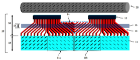
도 1b는 도 1a의 배향층에 의한 빛샘을 나타낸 도면이다.
도 2는 본원의 일 실시예에 따른 액정표시장치를 나타낸 단면도이다.
도 3은 도 2의 표시영역 중 일부를 나타낸 단면도이다.
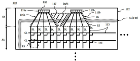
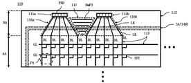
도 4는 도 2의 박막트랜지스터 어레이 기판 중 일부를 나타낸 도면이다.
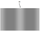
도 5는 도 2의 제 1 배향층을 나타낸 도면이다.
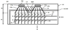
도 6 내지 도 8은 본원의 일 실시예에 따른 더미패턴의 다른 예시를 나타낸 도면이다.
NA: 비표시영역 110: 박막트랜지스터 어레이 기판
120: 컬러필터 어레이 기판 130: 액정층
140: 실링층 111, 121: 제 1 및 제 2 배향층
112: 제 1 기판 113: 박막트랜지스터 어레이
114: 보호층 122: 제 2 기판
123: 블랙매트릭스 124: 컬러필터
150: 백라이트유닛 SA: 실링영역
GL: 게이트라인 DL: 데이터라인
PA: 화소영역 TFT: 박막트랜지스터
115a, 115b: 패드영역 PAD: 패드
116a, 116b: 링크영역 LINK: 링크
117: 간격영역 DmP1, DmP2, DmP3, DmP4: 더미패턴
Claims (6)
- 화상이 표시되는 표시영역과, 그 외곽의 비표시영역을 포함하는 액정표시장치에 있어서,
상기 표시영역과 대응하여 복수의 화소영역을 정의하도록, 제 1 기판 상의 상기 표시영역에 상호 교차하는 방향으로 형성되는 게이트라인과 데이터라인;
상기 제 1 기판 상의 상기 비표시영역 중 둘 이상의 패드영역 각각에, 외부 회로의 접속 단자로 형성되는 적어도 하나의 패드;
상기 제 1 기판 상의 상기 비표시영역 중 둘 이상의 링크영역 각각에, 상기 게이트라인과 데이터라인 중 어느 하나와 상기 각 패드 사이를 연결하도록 형성되는 적어도 하나의 링크;
상기 제 1 기판 상의 상기 비표시영역 중 두 개의 상기 링크영역 사이인 간격영역에, 단일방향의 직선형태로 형성되는 적어도 하나의 더미패턴을 포함하는 액정표시장치. - 제 1 항에 있어서,
상기 더미패턴은
상기 게이트라인의 방향 및 데이터라인의 방향에 비스듬한 직선형태로 형성되는 액정표시장치. - 제 1 항에 있어서,
상기 더미패턴은
상기 게이트라인 및 상기 데이터라인 중 어느 하나의 방향에 평행한 직선형태로 형성되는 액정표시장치. - 제 1 항 내지 제 3 항 중 어느 한 항에 있어서,
상기 제 1 기판에 대향 합착되는 제 2 기판;
상기 제 1 및 제 2 기판 사이의 상기 비표시영역 중 실링영역에 형성되는 실링층; 및
상기 제 1 및 제 2 기판 각각의 서로 마주하는 일면 상에 형성되는 제 1 및 제 2 배향층; 및
상기 제 1 및 제 2 기판 사이에 주입되고 상기 실링층으로 밀봉되어 형성되는 액정층을 포함하고,
상기 액정층은 상기 제 1 및 제 2 배향층과 접하여, 상기 제 1 및 제 2 배향층에 의해 배향되는 액정표시장치. - 제 4 항에 있어서,
상기 제 1 기판 상의 상기 표시영역 중 상기 게이트라인과 데이터라인 사이의 교차영역에, 상기 복수의 화소영역과 대응하도록 형성되는 복수의 박막트랜지스터; 및
상기 제 1 기판 상의 상기 표시영역에 상기 복수의 화소영역과 대응하도록 형성되고, 상기 복수의 박막트랜지스터와 연결되는 복수의 화소전극을 더 포함하는 액정표시장치. - 제 5 항에 있어서,
상기 제 2 기판 상의 상기 표시영역에 상기 각 화소영역의 외곽과 대응하도록 형성되는 블랙매트릭스; 및
상기 제 2 기판 상의 상기 표시영역에 상기 각 화소영역과 대응하도록 형성되는 컬러필터를 더 포함하는 액정표시장치.
Priority Applications (1)
| Application Number | Priority Date | Filing Date | Title |
|---|---|---|---|
| KR1020130010242A KR20140097774A (ko) | 2013-01-30 | 2013-01-30 | 액정표시장치 |
Applications Claiming Priority (1)
| Application Number | Priority Date | Filing Date | Title |
|---|---|---|---|
| KR1020130010242A KR20140097774A (ko) | 2013-01-30 | 2013-01-30 | 액정표시장치 |
Publications (1)
| Publication Number | Publication Date |
|---|---|
| KR20140097774A true KR20140097774A (ko) | 2014-08-07 |
Family
ID=51744907
Family Applications (1)
| Application Number | Title | Priority Date | Filing Date |
|---|---|---|---|
| KR1020130010242A Ceased KR20140097774A (ko) | 2013-01-30 | 2013-01-30 | 액정표시장치 |
Country Status (1)
| Country | Link |
|---|---|
| KR (1) | KR20140097774A (ko) |
Cited By (6)
| Publication number | Priority date | Publication date | Assignee | Title |
|---|---|---|---|---|
| WO2016119338A1 (zh) * | 2015-01-27 | 2016-08-04 | 京东方科技集团股份有限公司 | 阵列基板以及显示装置 |
| CN109375441A (zh) * | 2018-12-21 | 2019-02-22 | 信利半导体有限公司 | 基板走线结构和走线制作方法 |
| KR20190038149A (ko) * | 2017-09-29 | 2019-04-08 | 엘지디스플레이 주식회사 | 유기발광 표시장치 |
| CN109597255A (zh) * | 2018-12-24 | 2019-04-09 | 惠科股份有限公司 | 一种显示面板、制程方法以及显示装置 |
| CN110333633A (zh) * | 2019-05-29 | 2019-10-15 | 重庆惠科金渝光电科技有限公司 | 阵列基板及显示面板 |
| WO2024222275A1 (zh) * | 2023-04-28 | 2024-10-31 | 京东方科技集团股份有限公司 | 一种显示基板、显示面板及显示装置 |
-
2013
- 2013-01-30 KR KR1020130010242A patent/KR20140097774A/ko not_active Ceased
Cited By (8)
| Publication number | Priority date | Publication date | Assignee | Title |
|---|---|---|---|---|
| WO2016119338A1 (zh) * | 2015-01-27 | 2016-08-04 | 京东方科技集团股份有限公司 | 阵列基板以及显示装置 |
| US9766500B2 (en) | 2015-01-27 | 2017-09-19 | Boe Technology Group Co., Ltd. | Array substrate and display device |
| KR20190038149A (ko) * | 2017-09-29 | 2019-04-08 | 엘지디스플레이 주식회사 | 유기발광 표시장치 |
| CN109375441A (zh) * | 2018-12-21 | 2019-02-22 | 信利半导体有限公司 | 基板走线结构和走线制作方法 |
| CN109597255A (zh) * | 2018-12-24 | 2019-04-09 | 惠科股份有限公司 | 一种显示面板、制程方法以及显示装置 |
| CN110333633A (zh) * | 2019-05-29 | 2019-10-15 | 重庆惠科金渝光电科技有限公司 | 阵列基板及显示面板 |
| CN110333633B (zh) * | 2019-05-29 | 2022-01-25 | 重庆惠科金渝光电科技有限公司 | 阵列基板及显示面板 |
| WO2024222275A1 (zh) * | 2023-04-28 | 2024-10-31 | 京东方科技集团股份有限公司 | 一种显示基板、显示面板及显示装置 |
Similar Documents
| Publication | Publication Date | Title |
|---|---|---|
| US8582070B2 (en) | Array substrate for multi-vision and liquid crystal display device including the same | |
| KR101987094B1 (ko) | 표시 장치 및 이의 제조 방법 | |
| KR102204976B1 (ko) | 표시 장치 및 그것의 제조 방법 | |
| JP2015148699A (ja) | 表示装置及びその製造方法 | |
| KR20160100134A (ko) | 액정 표시 장치 및 액정 표시 장치의 제조 방법 | |
| US9726947B2 (en) | Liquid crystal display device | |
| KR20140057015A (ko) | 나노 크리스탈 디스플레이 | |
| US10310334B2 (en) | Display device and method of producing display device | |
| US20110222015A1 (en) | Liquid crystal display | |
| US10162206B2 (en) | Liquid crystal display device | |
| US9470936B2 (en) | Liquid crystal display device | |
| US8773630B2 (en) | Display device | |
| US20150042912A1 (en) | Liquid crystal display apparatus | |
| JP2017181816A (ja) | 表示装置、液晶表示装置、及び表示装置の製造方法 | |
| KR102426496B1 (ko) | 액정표시장치 | |
| KR20040103275A (ko) | 횡전계 방식 액정표시장치 및 제조 방법 | |
| KR102434032B1 (ko) | 배리어패널 및 이를 포함하는 표시장치 | |
| KR102814938B1 (ko) | 표시 장치 | |
| KR20130026473A (ko) | 전기영동표시장치 및 그 제조방법 | |
| KR100841629B1 (ko) | 횡전계모드 액정표시소자 | |
| KR20070044918A (ko) | 액정패널 및 그 제조방법 | |
| KR101980772B1 (ko) | 2 픽셀 2 도메인 액정표시장치 | |
| US20160363827A1 (en) | Liquid crystal displays and the vertical alignment liquid crystal panels thereof | |
| CN106610549A (zh) | 显示装置 | |
| KR102531533B1 (ko) | 표시장치 |
Legal Events
| Date | Code | Title | Description |
|---|---|---|---|
| PA0109 | Patent application |
Patent event code: PA01091R01D Comment text: Patent Application Patent event date: 20130130 |
|
| PG1501 | Laying open of application | ||
| A201 | Request for examination | ||
| PA0201 | Request for examination |
Patent event code: PA02012R01D Patent event date: 20180111 Comment text: Request for Examination of Application Patent event code: PA02011R01I Patent event date: 20130130 Comment text: Patent Application |
|
| E902 | Notification of reason for refusal | ||
| PE0902 | Notice of grounds for rejection |
Comment text: Notification of reason for refusal Patent event date: 20190221 Patent event code: PE09021S01D |
|
| E601 | Decision to refuse application | ||
| PE0601 | Decision on rejection of patent |
Patent event date: 20190429 Comment text: Decision to Refuse Application Patent event code: PE06012S01D Patent event date: 20190221 Comment text: Notification of reason for refusal Patent event code: PE06011S01I |