KR20140100143A - 비휘발성 메모리 장치의 프로그램 방법 및 읽기 방법 - Google Patents
비휘발성 메모리 장치의 프로그램 방법 및 읽기 방법 Download PDFInfo
- Publication number
- KR20140100143A KR20140100143A KR1020130013033A KR20130013033A KR20140100143A KR 20140100143 A KR20140100143 A KR 20140100143A KR 1020130013033 A KR1020130013033 A KR 1020130013033A KR 20130013033 A KR20130013033 A KR 20130013033A KR 20140100143 A KR20140100143 A KR 20140100143A
- Authority
- KR
- South Korea
- Prior art keywords
- bit lines
- data
- program
- word line
- latches
- Prior art date
- Legal status (The legal status is an assumption and is not a legal conclusion. Google has not performed a legal analysis and makes no representation as to the accuracy of the status listed.)
- Ceased
Links
Images



Classifications
-
- G—PHYSICS
- G11—INFORMATION STORAGE
- G11C—STATIC STORES
- G11C7/00—Arrangements for writing information into, or reading information out from, a digital store
- G11C7/12—Bit line control circuits, e.g. drivers, boosters, pull-up circuits, pull-down circuits, precharging circuits, equalising circuits, for bit lines
-
- G—PHYSICS
- G11—INFORMATION STORAGE
- G11C—STATIC STORES
- G11C16/00—Erasable programmable read-only memories
- G11C16/02—Erasable programmable read-only memories electrically programmable
- G11C16/06—Auxiliary circuits, e.g. for writing into memory
- G11C16/10—Programming or data input circuits
-
- G—PHYSICS
- G11—INFORMATION STORAGE
- G11C—STATIC STORES
- G11C16/00—Erasable programmable read-only memories
- G11C16/02—Erasable programmable read-only memories electrically programmable
- G11C16/06—Auxiliary circuits, e.g. for writing into memory
- G11C16/24—Bit-line control circuits
-
- G—PHYSICS
- G11—INFORMATION STORAGE
- G11C—STATIC STORES
- G11C16/00—Erasable programmable read-only memories
- G11C16/02—Erasable programmable read-only memories electrically programmable
- G11C16/06—Auxiliary circuits, e.g. for writing into memory
- G11C16/26—Sensing or reading circuits; Data output circuits
-
- G—PHYSICS
- G11—INFORMATION STORAGE
- G11C—STATIC STORES
- G11C16/00—Erasable programmable read-only memories
- G11C16/02—Erasable programmable read-only memories electrically programmable
- G11C16/06—Auxiliary circuits, e.g. for writing into memory
- G11C16/34—Determination of programming status, e.g. threshold voltage, overprogramming or underprogramming, retention
-
- G—PHYSICS
- G11—INFORMATION STORAGE
- G11C—STATIC STORES
- G11C16/00—Erasable programmable read-only memories
- G11C16/02—Erasable programmable read-only memories electrically programmable
- G11C16/06—Auxiliary circuits, e.g. for writing into memory
- G11C16/34—Determination of programming status, e.g. threshold voltage, overprogramming or underprogramming, retention
- G11C16/3436—Arrangements for verifying correct programming or erasure
- G11C16/3454—Arrangements for verifying correct programming or for detecting overprogrammed cells
- G11C16/3459—Circuits or methods to verify correct programming of nonvolatile memory cells
-
- G—PHYSICS
- G11—INFORMATION STORAGE
- G11C—STATIC STORES
- G11C7/00—Arrangements for writing information into, or reading information out from, a digital store
- G11C7/06—Sense amplifiers; Associated circuits, e.g. timing or triggering circuits
- G11C7/065—Differential amplifiers of latching type
Landscapes
- Read Only Memory (AREA)
Abstract
Description
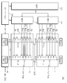
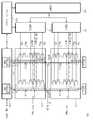
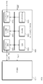
도 2는 도 1에 도시된 비휘발성 메모리 장치의 프로그램 동작을 개략적으로 설명하기 위한 도면이다.
도 3은 도 1에 도시된 비휘발성 메모리 장치의 프로그램 방법에 대한 실시 예를 보여주는 흐름도이다.
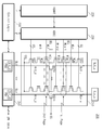
도 4는 도 1에 도시된 비휘발성 메모리 장치의 읽기 동작을 개략적으로 설명하기 위한 도면이다.
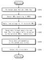
도 5는 본 발명의 실시 예에 따른 비휘발성 메모리 장치의 읽기 방법을 예시적으로 보여주는 흐름도이다.
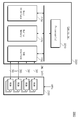
도 6은 본 발명의 다른 실시 예에 따른 메모리 장치를 예시적으로 보여주는 도면이다.
도 7은 본 발명에 따른 메모리 시스템을 예시적으로 보여주는 블록도이다.
도 8은 본 발명의 실시 예에 따른 SSD를 예시적으로 보여주는 블록도이다.
도 9는 본 발명에 따른 eMMC를 예시적으로 보여주는 블록도이다.
110: 메모리 셀 어레이
120: 전압 발생 회로
130: 어드레스 디코더
140: 입출력 회로
150: 제어 로직
PB0 ~ PBn: 페이지 버퍼
SL0_u ~ SLn_u: 상부 감지 래치
SL0_d ~ SLn_d: 하부 감지 래치
BST0 ~ BSTn: 비트라인 공유 트랜지스터
BLSS: 비트라인 공유 신호
BL0_u ~ BLn_u: 상부 비트라인
BL0_d ~ BLn_d: 하부 비트라인
WL0 ~ WLm: 워드라인
Claims (10)
- 비휘발성 메모리 장치의 프로그램 방법에 있어서:
제 1 워드라인에 연결된 제 1 메모리 셀들에 저장될 제 1 워드라인 데이터 및 제 2 워드라인에 연결된 제 2 메모리 셀들에 저장될 제 2 워드라인 데이터를 로딩하는 단계;
상기 제 1 워드라인 데이터에 따라 상부 비트라인들을 설정하는 단계;
상기 상부 비트라인들을 설정한 후, 비트라인 공유 트랜지스터들을 턴오프시키고 상기 제 2 워드라인 데이터에 따라 하부 비트라인들을 설정하는 단계;
상기 상부 비트라인들의 전압들을 이용하여 상기 제 1 메모리 셀들에 제 1 프로그램 동작을 수행하는 단계;
상기 비트라인 공유 트랜지스터들을 턴온시키고 상기 하부 비트라인들의 전압들을 이용하여 상기 제 2 메모리 셀들에 제 2 프로그램 동작을 수행하는 단계를 포함하고,
상기 비트라인 공유 트랜지스터들은 비트라인 공유 신호에 응답하여 상기 상부 비트라인들과 상기 하부 비트라인들을 전기적으로 연결하는 프로그램 방법. - 제 1 항에 있어서,
상기 제 1 프로그램 동작을 수행하는 단계는,
상기 제 1 워드라인으로 프로그램 펄스를 인가하는 단계를 포함하고,
상기 제 2 프로그램 동작을 수행하는 단계는,
상기 제 2 워드라인으로 상기 프로그램 펄스를 인가하는 단계를 포함하는 프로그램 방법. - 제 2 항에 있어서,
상기 제 1 프로그램 동작 및 상기 제 2 프로그램 동작이 동시에 수행되는 프로그램 방법. - 제 1 항에 있어서,
상기 제 1 메모리 셀들이 포함된 제 1 메모리 블록과 상기 제 2 메모리 셀들이 포함된 제 2 메모리 블록은 서로 분리되는 프로그램 방법. - 제 1 항에 있어서,
상기 제 1 및 제 2 프로그램 동작들을 수행한 뒤에 프로그램 검증 동작을 수행하는 단계를 더 포함하는 프로그램 방법. - 제 5 항에 있어서,
상기 프로그램 검증 동작이 실패하면, 사전에 결정된 값만큼 프로그램 펄스를 증가시킨 후, 상기 상부 비트라인들 및 상기 하부 비트라인들을 설정하고, 상기 제 1 및 제 2 프로그램 동작들을 반복하는 단계를 더 포함하는 프로그램 방법. - 제 1 항에 있어서,
상기 비트라인 공유 트랜지스터들 각각은 고전압용 트랜지스터인 프로그램 방법. - 비휘발성 메모리 장치의 읽기 방법에 있어서:
비트라인 공유 트랜지스터들을 턴온시키고 상부 비트라인들과 하부 비트라인들을 프리차지시키는 단계;
상기 상부 비트라인들 및 상기 하부 비트라인들을 프리차지시킨 후, 상기 비트라인 공유 트랜지스터들을 턴오프시키는 단계;
어드레스에 응답하여 선택된 제 1 및 제 2 워드라인들로 읽기 전압을 인가하는 단계;
상기 상부 비트라인들에 연결된 상부 감지 래치들을 통하여 상기 제 1 워드라인들에 연결된 제 1 메모리 셀들의 데이터를 감지하는 제 1 감지 단계;
상기 비트라인 공유 트랜지스터들을 턴오프시키고 상기 하부 비트라인들에 연결된 하부 감지 래치들을 통하여 상기 제 2 워드라인들에 연결된 제 2 메모리 셀들의 데이터를 감지하는 제 2 감지 단계;
상기 상부 감지 래치들에 저장된 데이터 및 상기 하부 감지 래치들에 저장된 데이터에 대응하는 데이터를 데이터 래치들에 저장하는 단계; 및
상기 데이터 래치들에 저장된 데이터를 외부로 출력하는 단계를 포함하고,
상기 비트라인 공유 트랜지스터들은 비트라인 공유 신호에 응답하여 상기 상부 비트라인들과 상기 하부 비트라인들을 전기적으로 연결하는 읽기 방법. - 제 8 항에 있어서,
상기 비휘발성 메모리 장치는 제 1 및 제 2 메모리 셀들을 갖는 메모리 셀 어레이를 포함하고,
상기 상부 감지 래치들은 상기 메모리 셀 어레이의 상부에 배치되고,
상기 데이터 래치들 및 상기 하부 감지 래치들은 상기 메모리 셀 어레이의 하부에 배치되는 읽기 방법. - 제 8 항에 있어서,
상기 상부 비트라인들 각각에 스트링이 연결되고,
상기 스트링은, 직렬 연결된 적어도 하나의 스트링 선택 트랜지스터, 복수의 메모리 셀들, 및 적어도 하나의 접지 선택 트랜지스터를 포함하는 읽기 방법.
Priority Applications (3)
| Application Number | Priority Date | Filing Date | Title |
|---|---|---|---|
| KR1020130013033A KR20140100143A (ko) | 2013-02-05 | 2013-02-05 | 비휘발성 메모리 장치의 프로그램 방법 및 읽기 방법 |
| US14/151,534 US9396797B2 (en) | 2013-02-05 | 2014-01-09 | Program methods of memory devices using bit line sharing |
| US15/188,461 US9633704B2 (en) | 2013-02-05 | 2016-06-21 | Read methods of memory devices using bit line sharing |
Applications Claiming Priority (1)
| Application Number | Priority Date | Filing Date | Title |
|---|---|---|---|
| KR1020130013033A KR20140100143A (ko) | 2013-02-05 | 2013-02-05 | 비휘발성 메모리 장치의 프로그램 방법 및 읽기 방법 |
Publications (1)
| Publication Number | Publication Date |
|---|---|
| KR20140100143A true KR20140100143A (ko) | 2014-08-14 |
Family
ID=51259102
Family Applications (1)
| Application Number | Title | Priority Date | Filing Date |
|---|---|---|---|
| KR1020130013033A Ceased KR20140100143A (ko) | 2013-02-05 | 2013-02-05 | 비휘발성 메모리 장치의 프로그램 방법 및 읽기 방법 |
Country Status (2)
| Country | Link |
|---|---|
| US (2) | US9396797B2 (ko) |
| KR (1) | KR20140100143A (ko) |
Cited By (1)
| Publication number | Priority date | Publication date | Assignee | Title |
|---|---|---|---|---|
| US10121543B2 (en) | 2015-08-21 | 2018-11-06 | Samsung Electronics Co., Ltd. | Storage device including a nonvolatile memory device and a controller for controlling a write operation of the nonvolatile memory device and an operating method of the storage device |
Families Citing this family (11)
| Publication number | Priority date | Publication date | Assignee | Title |
|---|---|---|---|---|
| US8860117B2 (en) | 2011-04-28 | 2014-10-14 | Micron Technology, Inc. | Semiconductor apparatus with multiple tiers of memory cells with peripheral transistors, and methods |
| US8964474B2 (en) | 2012-06-15 | 2015-02-24 | Micron Technology, Inc. | Architecture for 3-D NAND memory |
| US9362300B2 (en) * | 2014-10-08 | 2016-06-07 | Micron Technology, Inc. | Apparatuses and methods for forming multiple decks of memory cells |
| KR102340328B1 (ko) * | 2016-01-07 | 2021-12-16 | 에스케이하이닉스 주식회사 | 반도체 메모리 장치 및 이의 동작 방법 |
| US9679650B1 (en) | 2016-05-06 | 2017-06-13 | Micron Technology, Inc. | 3D NAND memory Z-decoder |
| US10074430B2 (en) * | 2016-08-08 | 2018-09-11 | Micron Technology, Inc. | Multi-deck memory device with access line and data line segregation between decks and method of operation thereof |
| KR102649347B1 (ko) * | 2016-10-11 | 2024-03-20 | 삼성전자주식회사 | 불휘발성 메모리 장치를 프로그램하는 방법과, 상기 메모리 장치를 포함하는 시스템의 작동 방법 |
| KR102743810B1 (ko) * | 2019-06-10 | 2024-12-18 | 에스케이하이닉스 주식회사 | 반도체 장치 및 반도체 장치의 동작 방법 |
| US11450381B2 (en) | 2019-08-21 | 2022-09-20 | Micron Technology, Inc. | Multi-deck memory device including buffer circuitry under array |
| US11189335B2 (en) | 2019-11-13 | 2021-11-30 | Sandisk Technologies Llc | Double write/read throughput by CMOS adjacent array (CaA) NAND memory |
| KR20250058267A (ko) * | 2023-10-23 | 2025-04-30 | 에스케이하이닉스 주식회사 | 반도체 장치 |
Family Cites Families (14)
| Publication number | Priority date | Publication date | Assignee | Title |
|---|---|---|---|---|
| KR100948483B1 (ko) | 2003-04-01 | 2010-03-18 | 주식회사 하이닉스반도체 | 반도체 메모리 장치 |
| JP4654671B2 (ja) | 2004-11-29 | 2011-03-23 | ソニー株式会社 | 半導体記憶装置 |
| US7313023B2 (en) | 2005-03-11 | 2007-12-25 | Sandisk Corporation | Partition of non-volatile memory array to reduce bit line capacitance |
| KR100742278B1 (ko) | 2005-11-23 | 2007-07-24 | 삼성전자주식회사 | 향상된 동작 속도 및 듀얼 프로그램 기능을 갖는 낸드플래시 메모리 장치 |
| EP1814123A1 (en) | 2006-01-26 | 2007-08-01 | Samsung Electronics Co.,Ltd. | Nand-type nonvolatile memory device having common bit lines and methods of operating the same |
| KR100666184B1 (ko) * | 2006-02-02 | 2007-01-09 | 삼성전자주식회사 | 하부 비트라인들과 상부 비트라인들이 전압제어블락을공유하는 3-레벨 불휘발성 반도체 메모리 장치 |
| JP2007293986A (ja) | 2006-04-24 | 2007-11-08 | Toshiba Corp | 半導体記憶装置 |
| KR100854972B1 (ko) * | 2007-02-13 | 2008-08-28 | 삼성전자주식회사 | 메모리 시스템 및 그것의 데이터 읽기 방법 |
| US7706184B2 (en) | 2007-12-28 | 2010-04-27 | Kabushiki Kaisha Toshiba | Nonvolatile semiconductor memory device |
| KR101462606B1 (ko) | 2008-10-08 | 2014-11-19 | 삼성전자주식회사 | 공통 비트 라인을 가지는 비휘발성 메모리 소자 |
| JP2011113619A (ja) | 2009-11-27 | 2011-06-09 | Toshiba Corp | Nand型フラッシュメモリ |
| JP2011198437A (ja) * | 2010-03-23 | 2011-10-06 | Toshiba Corp | 不揮発性半導体記憶装置 |
| US8331126B2 (en) | 2010-06-28 | 2012-12-11 | Qualcomm Incorporated | Non-volatile memory with split write and read bitlines |
| US8837216B2 (en) | 2010-12-13 | 2014-09-16 | Sandisk Technologies Inc. | Non-volatile storage system with shared bit lines connected to a single selection device |
-
2013
- 2013-02-05 KR KR1020130013033A patent/KR20140100143A/ko not_active Ceased
-
2014
- 2014-01-09 US US14/151,534 patent/US9396797B2/en active Active
-
2016
- 2016-06-21 US US15/188,461 patent/US9633704B2/en active Active
Cited By (1)
| Publication number | Priority date | Publication date | Assignee | Title |
|---|---|---|---|---|
| US10121543B2 (en) | 2015-08-21 | 2018-11-06 | Samsung Electronics Co., Ltd. | Storage device including a nonvolatile memory device and a controller for controlling a write operation of the nonvolatile memory device and an operating method of the storage device |
Also Published As
| Publication number | Publication date |
|---|---|
| US9633704B2 (en) | 2017-04-25 |
| US20140219025A1 (en) | 2014-08-07 |
| US9396797B2 (en) | 2016-07-19 |
| US20160300601A1 (en) | 2016-10-13 |
Similar Documents
| Publication | Publication Date | Title |
|---|---|---|
| US10297299B2 (en) | Semiconductor device and operating method thereof | |
| KR20140100143A (ko) | 비휘발성 메모리 장치의 프로그램 방법 및 읽기 방법 | |
| KR102233810B1 (ko) | 비휘발성 메모리 장치 및 그것의 워드라인 구동 방법 | |
| US10573378B2 (en) | Methods of programming memory devices | |
| CN106157999B (zh) | 包括虚设存储单元的半导体存储器件及其操作方法 | |
| KR101857529B1 (ko) | 비휘발성 메모리 장치 및 그것의 구동 방법 | |
| US8891315B2 (en) | Nonvolatile memory device and erase method thereof | |
| TWI725296B (zh) | 記憶體裝置及其操作方法 | |
| KR102248835B1 (ko) | 불 휘발성 메모리 장치 및 그것의 동작 방법 | |
| US10360978B2 (en) | Semiconductor memory device for performing coding program and operating method thereof | |
| TWI681398B (zh) | 半導體記憶體裝置及其操作方法 | |
| KR20190019427A (ko) | 메모리 장치 및 그 동작 방법 | |
| US8902666B2 (en) | Programming method for nonvolatile memory device | |
| US20150279469A1 (en) | Nonvolatile memory device, program method thereof, and data processing system including the same | |
| KR20180001303A (ko) | 메모리 시스템 및 그 동작 방법 | |
| KR20180028292A (ko) | 반도체 메모리 장치 및 그것의 동작 방법 | |
| US10141066B2 (en) | Memory device and operating method thereof | |
| US20180190358A1 (en) | Semiconductor memory device and method of operating the same | |
| CN110058799A (zh) | 存储器装置及操作存储器装置的方法 | |
| US11842773B2 (en) | Page buffer, semiconductor memory device with page buffer, and method of operating semiconductor memory device | |
| KR102133362B1 (ko) | 비휘발성 메모리 장치, 그것을 포함하는 메모리 시스템, 및 그것의 프로그램 방법 | |
| US11646089B2 (en) | Memory device for performing verify operation and operating method thereof | |
| CN113257320B (zh) | 非易失性存储器设备 | |
| US20230307069A1 (en) | Memory device and method of operating the same | |
| US20260011370A1 (en) | Double single level cell program in a memory device |
Legal Events
| Date | Code | Title | Description |
|---|---|---|---|
| PA0109 | Patent application |
Patent event code: PA01091R01D Comment text: Patent Application Patent event date: 20130205 |
|
| PG1501 | Laying open of application | ||
| A201 | Request for examination | ||
| PA0201 | Request for examination |
Patent event code: PA02012R01D Patent event date: 20180111 Comment text: Request for Examination of Application Patent event code: PA02011R01I Patent event date: 20130205 Comment text: Patent Application |
|
| E902 | Notification of reason for refusal | ||
| PE0902 | Notice of grounds for rejection |
Comment text: Notification of reason for refusal Patent event date: 20190630 Patent event code: PE09021S01D |
|
| AMND | Amendment | ||
| E601 | Decision to refuse application | ||
| PE0601 | Decision on rejection of patent |
Patent event date: 20191224 Comment text: Decision to Refuse Application Patent event code: PE06012S01D Patent event date: 20190630 Comment text: Notification of reason for refusal Patent event code: PE06011S01I |
|
| X091 | Application refused [patent] | ||
| AMND | Amendment | ||
| PX0901 | Re-examination |
Patent event code: PX09011S01I Patent event date: 20191224 Comment text: Decision to Refuse Application Patent event code: PX09012R01I Patent event date: 20190819 Comment text: Amendment to Specification, etc. |
|
| PX0601 | Decision of rejection after re-examination |
Comment text: Decision to Refuse Application Patent event code: PX06014S01D Patent event date: 20200220 Comment text: Amendment to Specification, etc. Patent event code: PX06012R01I Patent event date: 20200122 Comment text: Decision to Refuse Application Patent event code: PX06011S01I Patent event date: 20191224 Comment text: Amendment to Specification, etc. Patent event code: PX06012R01I Patent event date: 20190819 Comment text: Notification of reason for refusal Patent event code: PX06013S01I Patent event date: 20190630 |
|
| X601 | Decision of rejection after re-examination | ||
| J201 | Request for trial against refusal decision | ||
| PJ0201 | Trial against decision of rejection |
Patent event date: 20200323 Comment text: Request for Trial against Decision on Refusal Patent event code: PJ02012R01D Patent event date: 20200220 Comment text: Decision to Refuse Application Patent event code: PJ02011S01I Patent event date: 20191224 Comment text: Decision to Refuse Application Patent event code: PJ02011S01I Appeal kind category: Appeal against decision to decline refusal Decision date: 20210722 Appeal identifier: 2020101000855 Request date: 20200323 |
|
| J301 | Trial decision |
Free format text: TRIAL NUMBER: 2020101000855; TRIAL DECISION FOR APPEAL AGAINST DECISION TO DECLINE REFUSAL REQUESTED 20200323 Effective date: 20210722 |
|
| PJ1301 | Trial decision |
Patent event code: PJ13011S01D Patent event date: 20210722 Comment text: Trial Decision on Objection to Decision on Refusal Appeal kind category: Appeal against decision to decline refusal Request date: 20200323 Decision date: 20210722 Appeal identifier: 2020101000855 |