KR20140107517A - 임프린트 장치 및 이를 이용한 물품의 제조 방법 - Google Patents
임프린트 장치 및 이를 이용한 물품의 제조 방법 Download PDFInfo
- Publication number
- KR20140107517A KR20140107517A KR1020147020115A KR20147020115A KR20140107517A KR 20140107517 A KR20140107517 A KR 20140107517A KR 1020147020115 A KR1020147020115 A KR 1020147020115A KR 20147020115 A KR20147020115 A KR 20147020115A KR 20140107517 A KR20140107517 A KR 20140107517A
- Authority
- KR
- South Korea
- Prior art keywords
- area
- heating
- region
- substrate
- mold
- Prior art date
- Legal status (The legal status is an assumption and is not a legal conclusion. Google has not performed a legal analysis and makes no representation as to the accuracy of the status listed.)
- Granted
Links
Images




Classifications
-
- H—ELECTRICITY
- H10—SEMICONDUCTOR DEVICES; ELECTRIC SOLID-STATE DEVICES NOT OTHERWISE PROVIDED FOR
- H10P—GENERIC PROCESSES OR APPARATUS FOR THE MANUFACTURE OR TREATMENT OF DEVICES COVERED BY CLASS H10
- H10P76/00—Manufacture or treatment of masks on semiconductor bodies, e.g. by lithography or photolithography
- H10P76/20—Manufacture or treatment of masks on semiconductor bodies, e.g. by lithography or photolithography of masks comprising organic materials
- H10P76/204—Manufacture or treatment of masks on semiconductor bodies, e.g. by lithography or photolithography of masks comprising organic materials of organic photoresist masks
- H10P76/2041—Photolithographic processes
-
- G—PHYSICS
- G03—PHOTOGRAPHY; CINEMATOGRAPHY; ANALOGOUS TECHNIQUES USING WAVES OTHER THAN OPTICAL WAVES; ELECTROGRAPHY; HOLOGRAPHY
- G03F—PHOTOMECHANICAL PRODUCTION OF TEXTURED OR PATTERNED SURFACES, e.g. FOR PRINTING, FOR PROCESSING OF SEMICONDUCTOR DEVICES; MATERIALS THEREFOR; ORIGINALS THEREFOR; APPARATUS SPECIALLY ADAPTED THEREFOR
- G03F7/00—Photomechanical, e.g. photolithographic, production of textured or patterned surfaces, e.g. printing surfaces; Materials therefor, e.g. comprising photoresists; Apparatus specially adapted therefor
- G03F7/0002—Lithographic processes using patterning methods other than those involving the exposure to radiation, e.g. by stamping
-
- B—PERFORMING OPERATIONS; TRANSPORTING
- B29—WORKING OF PLASTICS; WORKING OF SUBSTANCES IN A PLASTIC STATE IN GENERAL
- B29C—SHAPING OR JOINING OF PLASTICS; SHAPING OF MATERIAL IN A PLASTIC STATE, NOT OTHERWISE PROVIDED FOR; AFTER-TREATMENT OF THE SHAPED PRODUCTS, e.g. REPAIRING
- B29C59/00—Surface shaping of articles, e.g. embossing; Apparatus therefor
- B29C59/002—Component parts, details or accessories; Auxiliary operations
-
- B—PERFORMING OPERATIONS; TRANSPORTING
- B29—WORKING OF PLASTICS; WORKING OF SUBSTANCES IN A PLASTIC STATE IN GENERAL
- B29C—SHAPING OR JOINING OF PLASTICS; SHAPING OF MATERIAL IN A PLASTIC STATE, NOT OTHERWISE PROVIDED FOR; AFTER-TREATMENT OF THE SHAPED PRODUCTS, e.g. REPAIRING
- B29C59/00—Surface shaping of articles, e.g. embossing; Apparatus therefor
- B29C59/16—Surface shaping of articles, e.g. embossing; Apparatus therefor by wave energy or particle radiation, e.g. infrared heating
-
- B—PERFORMING OPERATIONS; TRANSPORTING
- B82—NANOTECHNOLOGY
- B82Y—SPECIFIC USES OR APPLICATIONS OF NANOSTRUCTURES; MEASUREMENT OR ANALYSIS OF NANOSTRUCTURES; MANUFACTURE OR TREATMENT OF NANOSTRUCTURES
- B82Y10/00—Nanotechnology for information processing, storage or transmission, e.g. quantum computing or single electron logic
-
- B—PERFORMING OPERATIONS; TRANSPORTING
- B82—NANOTECHNOLOGY
- B82Y—SPECIFIC USES OR APPLICATIONS OF NANOSTRUCTURES; MEASUREMENT OR ANALYSIS OF NANOSTRUCTURES; MANUFACTURE OR TREATMENT OF NANOSTRUCTURES
- B82Y40/00—Manufacture or treatment of nanostructures
-
- G—PHYSICS
- G03—PHOTOGRAPHY; CINEMATOGRAPHY; ANALOGOUS TECHNIQUES USING WAVES OTHER THAN OPTICAL WAVES; ELECTROGRAPHY; HOLOGRAPHY
- G03F—PHOTOMECHANICAL PRODUCTION OF TEXTURED OR PATTERNED SURFACES, e.g. FOR PRINTING, FOR PROCESSING OF SEMICONDUCTOR DEVICES; MATERIALS THEREFOR; ORIGINALS THEREFOR; APPARATUS SPECIALLY ADAPTED THEREFOR
- G03F9/00—Registration or positioning of originals, masks, frames, photographic sheets or textured or patterned surfaces, e.g. automatically
- G03F9/70—Registration or positioning of originals, masks, frames, photographic sheets or textured or patterned surfaces, e.g. automatically for microlithography
- G03F9/7003—Alignment type or strategy, e.g. leveling, global alignment
-
- G—PHYSICS
- G03—PHOTOGRAPHY; CINEMATOGRAPHY; ANALOGOUS TECHNIQUES USING WAVES OTHER THAN OPTICAL WAVES; ELECTROGRAPHY; HOLOGRAPHY
- G03F—PHOTOMECHANICAL PRODUCTION OF TEXTURED OR PATTERNED SURFACES, e.g. FOR PRINTING, FOR PROCESSING OF SEMICONDUCTOR DEVICES; MATERIALS THEREFOR; ORIGINALS THEREFOR; APPARATUS SPECIALLY ADAPTED THEREFOR
- G03F9/00—Registration or positioning of originals, masks, frames, photographic sheets or textured or patterned surfaces, e.g. automatically
- G03F9/70—Registration or positioning of originals, masks, frames, photographic sheets or textured or patterned surfaces, e.g. automatically for microlithography
- G03F9/7003—Alignment type or strategy, e.g. leveling, global alignment
- G03F9/7042—Alignment for lithographic apparatus using patterning methods other than those involving the exposure to radiation, e.g. by stamping or imprinting
-
- G—PHYSICS
- G03—PHOTOGRAPHY; CINEMATOGRAPHY; ANALOGOUS TECHNIQUES USING WAVES OTHER THAN OPTICAL WAVES; ELECTROGRAPHY; HOLOGRAPHY
- G03F—PHOTOMECHANICAL PRODUCTION OF TEXTURED OR PATTERNED SURFACES, e.g. FOR PRINTING, FOR PROCESSING OF SEMICONDUCTOR DEVICES; MATERIALS THEREFOR; ORIGINALS THEREFOR; APPARATUS SPECIALLY ADAPTED THEREFOR
- G03F9/00—Registration or positioning of originals, masks, frames, photographic sheets or textured or patterned surfaces, e.g. automatically
- G03F9/70—Registration or positioning of originals, masks, frames, photographic sheets or textured or patterned surfaces, e.g. automatically for microlithography
- G03F9/7065—Production of alignment light, e.g. light source, control of coherence, polarization, pulse length, wavelength
-
- B—PERFORMING OPERATIONS; TRANSPORTING
- B29—WORKING OF PLASTICS; WORKING OF SUBSTANCES IN A PLASTIC STATE IN GENERAL
- B29C—SHAPING OR JOINING OF PLASTICS; SHAPING OF MATERIAL IN A PLASTIC STATE, NOT OTHERWISE PROVIDED FOR; AFTER-TREATMENT OF THE SHAPED PRODUCTS, e.g. REPAIRING
- B29C59/00—Surface shaping of articles, e.g. embossing; Apparatus therefor
- B29C59/02—Surface shaping of articles, e.g. embossing; Apparatus therefor by mechanical means, e.g. pressing
- B29C59/022—Surface shaping of articles, e.g. embossing; Apparatus therefor by mechanical means, e.g. pressing characterised by the disposition or the configuration, e.g. dimensions, of the embossments or the shaping tools therefor
- B29C2059/023—Microembossing
Landscapes
- Engineering & Computer Science (AREA)
- Physics & Mathematics (AREA)
- Nanotechnology (AREA)
- Chemical & Material Sciences (AREA)
- General Physics & Mathematics (AREA)
- Crystallography & Structural Chemistry (AREA)
- Condensed Matter Physics & Semiconductors (AREA)
- Manufacturing & Machinery (AREA)
- Mathematical Physics (AREA)
- Theoretical Computer Science (AREA)
- Toxicology (AREA)
- Health & Medical Sciences (AREA)
- Shaping Of Tube Ends By Bending Or Straightening (AREA)
- Exposure Of Semiconductors, Excluding Electron Or Ion Beam Exposure (AREA)
Abstract
Description
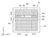
도 2는 제1 실시 형태에 따른 가열 영역 조정 기구의 구성을 나타내는 도면.
도 3은 임프린트 처리 시의 동작 시퀀스를 나타내는 플로우차트.
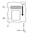
도 4a는 웨이퍼 상의 기판 측 패턴과 가열 영역을 나타내는 도면.
도 4b는 웨이퍼 상의 기판 측 패턴과 가열 영역을 나타내는 도면.
도 5는 기판 측 패턴의 1지점에서의 온도 변화를 나타내는 그래프.
도 6은 본 발명의 제3 실시 형태에 따른 임프린트 장치의 구성을 나타내는 도면.
도 7은 본 발명의 제4 실시 형태에 따른 임프린트 장치의 구성을 나타내는 도면.
Claims (12)
- 패턴이 형성된 패턴 영역을 포함하는 몰드를 이용하여 기판의 피처리 영역 상에 수지의 패턴을 형성하는 임프린트 장치이며,
상기 몰드 상의 패턴 영역 또는 상기 기판의 피처리 영역 중 어느 하나인 대상 영역의 형상을 보정하도록 구성된 보정 유닛을 포함하고,
상기 보정 유닛은,
상기 몰드 또는 상기 기판 중 상기 대상 영역에 대응하는 대상물을, 상기 몰드 상의 패턴 영역의 면적보다 작은 면적을 갖는 가열 영역에서 가열하도록 구성된 가열 유닛과,
상기 대상 영역과 상기 가열 영역의 상대 위치를 변화시킴으로써 상기 대상 영역에 대하여 상기 가열 영역을 주사하도록 구성된 주사 유닛과,
상기 대상 영역의 보정 변형량에 관한 정보를 취득하고, 상기 정보에 기초하여 상기 가열 유닛 및 상기 주사 유닛을 제어하도록 구성된 제어 유닛을 더 포함하는, 임프린트 장치. - 제1항에 있어서,
상기 가열 유닛은 상기 대상물에 부여되는 단위 시간 당 열량을 주사에 따라서 변화시키는, 임프린트 장치. - 제1항에 있어서,
상기 가열 유닛은 광원과, 상기 광원으로부터 방출되어 상기 대상물에 조사되는 광의 광량을 조정하는 광량 조정 유닛을 포함하는, 임프린트 장치. - 제3항에 있어서,
상기 광량 조정 유닛은 상기 광원과 상기 대상물 사이에 배치되고, 상기 광원으로부터 방출된 광의 일부를 차폐하는 이동가능한 차폐 부재를 포함하는, 임프린트 장치. - 제1항에 있어서,
상기 제어 유닛은, 상기 가열 영역이 상기 대상 영역의 외측에 위치된 상태에서 상기 주사 유닛이 주사를 개시하게 하는, 임프린트 장치. - 제1항에 있어서,
상기 주사 유닛은 상기 광원과 상기 대상물 사이에 배치되고, 상기 광원으로부터 방출된 광의 일부를 차폐하는 한 쌍의 이동가능한 차폐 부재를 포함하는, 임프린트 장치. - 제1항에 있어서,
상기 대상 영역은 상기 기판 상의 피처리 영역이며,
상기 주사 유닛은 상기 기판을 보유지지하면서 이동가능한 이동체를 구동시키도록 구성된 이동체 구동 유닛을 포함하는, 임프린트 장치. - 제6항에 있어서,
상기 몰드 상의 패턴 영역의 면적보다 작은 면적을 갖는 경화 영역에서 수지를 경화시키도록 구성되고, 상기 기판 상에 제공되는 경화 유닛을 더 포함하고,
상기 대상 영역은 상기 기판 상의 피처리 영역이며,
상기 가열 영역과 상기 경화 영역은 상기 기판 상에서 상기 주사 유닛의 주사 방향으로 서로 나란히 배치되고, 상기 주사 유닛에 의한 주사 시에, 상기 가열 영역이 상기 피처리 영역 위를 통과한 후에, 상기 경화 영역이 상기 피처리 영역 위를 통과하는, 임프린트 장치. - 제1항에 있어서,
복수의 토출구를 갖고, 상기 복수의 토출구를 통해서 토출되는 상기 수지를 상기 기판에 도포하는 도포 유닛을 더 포함하며,
상기 대상 영역은 상기 기판의 피처리 영역이며,
상기 가열 유닛은 상기 복수의 토출구로부터 토출되는 상기 수지를 가열하는 열원을 포함하는, 임프린트 장치. - 제1항에 있어서,
상기 보정 유닛은 상기 몰드에 힘을 가하는 복수의 액츄에이터를 더 포함하고,
상기 제어 유닛은 상기 몰드 상의 패턴 영역의 보정 변형량에 관한 제2 정보를 취득하고, 상기 제2 정보에 기초하여 상기 복수의 액츄에이터를 제어하는, 임프린트 장치. - 제1항에 있어서,
상기 기판에 상기 수지를 도포하도록 구성된 도포 유닛과,
상기 몰드를 보유지지하도록 구성된 몰드 보유지지 유닛과,
상기 기판을 보유지지하면서 이동가능하도록 구성된 이동체와,
상기 기판을 가열하도록 구성된 제2 가열 유닛을 더 포함하고,
상기 대상 영역은 상기 기판의 피처리 영역이며,
상기 제어 유닛은 상기 대상 영역의 보정 변형량에 관한 제1 가열 정보 및 제2 가열 정보를 취득하고, 상기 제1 가열 정보에 기초하여 상기 가열 유닛 및 상기 주사 유닛을 제어하고, 상기 제2 가열 정보에 기초하여 상기 제2 가열 유닛을 제어하는, 임프린트 장치. - 임프린트 장치를 이용하여 기판 상에 수지의 패턴을 형성하는 단계와,
상기 패턴이 형성된 기판을 가공하는 단계를 포함하고,
패턴이 형성된 패턴 영역을 포함하는 몰드를 이용하여 기판의 피처리 영역 상에 수지의 패턴을 형성하는, 상기 임프린트 장치는,
상기 몰드 상의 패턴 영역 또는 상기 기판의 피처리 영역 중 어느 하나인 대상 영역의 형상을 보정하도록 구성된 보정 유닛을 포함하고,
상기 보정 유닛은,
상기 몰드 또는 상기 기판 중 상기 대상 영역에 대응하는 대상물을, 상기 몰드 상의 패턴 영역의 면적보다 작은 면적을 갖는 가열 영역에서 가열하도록 구성된 가열 유닛과,
상기 대상 영역과 상기 가열 영역의 상대 위치를 변화시킴으로써 상기 대상 영역에 대하여 상기 가열 영역을 주사하도록 구성된 주사 유닛과,
상기 대상 영역의 보정 변형량에 관한 정보를 취득하고, 상기 정보에 기초하여 상기 가열 유닛 및 상기 주사 유닛을 제어하도록 구성된 제어 유닛을 더 포함하는, 물품의 제조 방법.
Applications Claiming Priority (5)
| Application Number | Priority Date | Filing Date | Title |
|---|---|---|---|
| JPJP-P-2012-015558 | 2012-01-27 | ||
| JP2012015558 | 2012-01-27 | ||
| JP2013006827A JP6045363B2 (ja) | 2012-01-27 | 2013-01-18 | インプリント装置、それを用いた物品の製造方法 |
| JPJP-P-2013-006827 | 2013-01-18 | ||
| PCT/JP2013/000400 WO2013111606A1 (en) | 2012-01-27 | 2013-01-25 | Imprint apparatus and article manufacturing method using same |
Publications (2)
| Publication Number | Publication Date |
|---|---|
| KR20140107517A true KR20140107517A (ko) | 2014-09-04 |
| KR101656161B1 KR101656161B1 (ko) | 2016-09-08 |
Family
ID=48873329
Family Applications (1)
| Application Number | Title | Priority Date | Filing Date |
|---|---|---|---|
| KR1020147020115A Active KR101656161B1 (ko) | 2012-01-27 | 2013-01-25 | 임프린트 장치 및 이를 이용한 물품의 제조 방법 |
Country Status (5)
| Country | Link |
|---|---|
| US (1) | US9851634B2 (ko) |
| JP (1) | JP6045363B2 (ko) |
| KR (1) | KR101656161B1 (ko) |
| CN (1) | CN104067373B (ko) |
| WO (1) | WO2013111606A1 (ko) |
Cited By (2)
| Publication number | Priority date | Publication date | Assignee | Title |
|---|---|---|---|---|
| KR20180108447A (ko) * | 2017-03-24 | 2018-10-04 | 캐논 가부시끼가이샤 | 리소그래피 장치, 및 물품 제조 방법 |
| KR20190134502A (ko) * | 2018-05-24 | 2019-12-04 | 캐논 가부시끼가이샤 | 임프린트 장치, 임프린트 방법 및 물품 제조 방법 |
Families Citing this family (15)
| Publication number | Priority date | Publication date | Assignee | Title |
|---|---|---|---|---|
| JP6329353B2 (ja) * | 2013-10-01 | 2018-05-23 | キヤノン株式会社 | インプリント装置、および物品の製造方法 |
| CN103522535B (zh) * | 2013-10-10 | 2015-09-09 | 无锡鑫宏业特塑线缆有限公司 | 手动热压痕标识设备 |
| JP6178694B2 (ja) * | 2013-10-17 | 2017-08-09 | キヤノン株式会社 | インプリント装置、および物品の製造方法 |
| KR101777905B1 (ko) | 2013-10-17 | 2017-09-12 | 캐논 가부시끼가이샤 | 임프린트 장치 그리고 물품을 제조하는 방법 |
| JP6611450B2 (ja) * | 2015-03-31 | 2019-11-27 | キヤノン株式会社 | インプリント装置、インプリント方法、及び物品の製造方法 |
| JP6797627B2 (ja) * | 2015-11-24 | 2020-12-09 | キヤノン株式会社 | インプリント装置、インプリント方法、および物品の製造方法 |
| US20170210036A1 (en) * | 2016-01-22 | 2017-07-27 | Canon Kabushiki Kaisha | Mold replicating method, imprint apparatus, and article manufacturing method |
| JP6732502B2 (ja) * | 2016-03-31 | 2020-07-29 | キヤノン株式会社 | 三次元造形方法、プログラム、記録媒体、及び三次元造形装置 |
| JP2017179575A (ja) * | 2016-03-31 | 2017-10-05 | キヤノン株式会社 | 三次元造形装置、及び三次元造形方法 |
| JP2017188556A (ja) * | 2016-04-05 | 2017-10-12 | キヤノン株式会社 | インプリント装置、インプリント方法、物品の製造方法、および型 |
| US11669009B2 (en) * | 2016-08-03 | 2023-06-06 | Board Of Regents, The University Of Texas System | Roll-to-roll programmable film imprint lithography |
| US10998190B2 (en) | 2017-04-17 | 2021-05-04 | Canon Kabushiki Kaisha | Imprint apparatus and method of manufacturing article |
| JP6606567B2 (ja) * | 2017-04-17 | 2019-11-13 | キヤノン株式会社 | インプリント装置及び物品の製造方法 |
| JP6921600B2 (ja) * | 2017-04-20 | 2021-08-18 | キヤノン株式会社 | インプリント装置、制御データの生成方法、及び物品の製造方法 |
| JP7121653B2 (ja) * | 2018-12-28 | 2022-08-18 | キヤノン株式会社 | 膜形成装置および物品製造方法 |
Citations (5)
| Publication number | Priority date | Publication date | Assignee | Title |
|---|---|---|---|---|
| JP2004259985A (ja) | 2003-02-26 | 2004-09-16 | Sony Corp | レジストパターン形成装置およびその形成方法、および、当該方法を用いた半導体装置の製造方法 |
| JP2004335808A (ja) * | 2003-05-08 | 2004-11-25 | Sony Corp | パターン転写装置、パターン転写方法およびプログラム |
| JP2007015375A (ja) * | 2005-06-08 | 2007-01-25 | Canon Inc | モールド、モールドを有する装置、パターン転写装置、及びパターン形成方法 |
| KR20090009874A (ko) * | 2006-04-18 | 2009-01-23 | 캐논 가부시끼가이샤 | 얼라인먼트방법, 임프린트방법, 얼라인먼트장치, 및 위치계측방법 |
| WO2009153925A1 (ja) | 2008-06-17 | 2009-12-23 | 株式会社ニコン | ナノインプリント方法及び装置 |
Family Cites Families (6)
| Publication number | Priority date | Publication date | Assignee | Title |
|---|---|---|---|---|
| JP2001060546A (ja) | 1999-08-20 | 2001-03-06 | Nikon Corp | 露光方法及び露光装置 |
| TW200500811A (en) | 2002-12-13 | 2005-01-01 | Molecular Imprints Inc | Magnification correction employing out-of-plane distortion of a substrate |
| US7927089B2 (en) | 2005-06-08 | 2011-04-19 | Canon Kabushiki Kaisha | Mold, apparatus including mold, pattern transfer apparatus, and pattern forming method |
| US7440076B2 (en) | 2005-09-29 | 2008-10-21 | Asml Netherlands B.V. | Lithographic apparatus, device manufacturing method and device manufactured thereby |
| JP4827513B2 (ja) | 2005-12-09 | 2011-11-30 | キヤノン株式会社 | 加工方法 |
| JP5442226B2 (ja) * | 2008-07-28 | 2014-03-12 | 株式会社Sokudo | 基板処理装置 |
-
2013
- 2013-01-18 JP JP2013006827A patent/JP6045363B2/ja active Active
- 2013-01-25 CN CN201380006253.3A patent/CN104067373B/zh active Active
- 2013-01-25 KR KR1020147020115A patent/KR101656161B1/ko active Active
- 2013-01-25 WO PCT/JP2013/000400 patent/WO2013111606A1/en not_active Ceased
- 2013-01-25 US US14/372,938 patent/US9851634B2/en active Active
Patent Citations (6)
| Publication number | Priority date | Publication date | Assignee | Title |
|---|---|---|---|---|
| JP2004259985A (ja) | 2003-02-26 | 2004-09-16 | Sony Corp | レジストパターン形成装置およびその形成方法、および、当該方法を用いた半導体装置の製造方法 |
| JP2004335808A (ja) * | 2003-05-08 | 2004-11-25 | Sony Corp | パターン転写装置、パターン転写方法およびプログラム |
| JP2007015375A (ja) * | 2005-06-08 | 2007-01-25 | Canon Inc | モールド、モールドを有する装置、パターン転写装置、及びパターン形成方法 |
| KR20090009874A (ko) * | 2006-04-18 | 2009-01-23 | 캐논 가부시끼가이샤 | 얼라인먼트방법, 임프린트방법, 얼라인먼트장치, 및 위치계측방법 |
| WO2009153925A1 (ja) | 2008-06-17 | 2009-12-23 | 株式会社ニコン | ナノインプリント方法及び装置 |
| US20110273684A1 (en) * | 2008-06-17 | 2011-11-10 | Nikon Corporation | Nano-imprint method and apparatus |
Cited By (2)
| Publication number | Priority date | Publication date | Assignee | Title |
|---|---|---|---|---|
| KR20180108447A (ko) * | 2017-03-24 | 2018-10-04 | 캐논 가부시끼가이샤 | 리소그래피 장치, 및 물품 제조 방법 |
| KR20190134502A (ko) * | 2018-05-24 | 2019-12-04 | 캐논 가부시끼가이샤 | 임프린트 장치, 임프린트 방법 및 물품 제조 방법 |
Also Published As
| Publication number | Publication date |
|---|---|
| CN104067373B (zh) | 2016-10-05 |
| JP6045363B2 (ja) | 2016-12-14 |
| WO2013111606A1 (en) | 2013-08-01 |
| US20150001751A1 (en) | 2015-01-01 |
| CN104067373A (zh) | 2014-09-24 |
| US9851634B2 (en) | 2017-12-26 |
| JP2013175709A (ja) | 2013-09-05 |
| KR101656161B1 (ko) | 2016-09-08 |
Similar Documents
| Publication | Publication Date | Title |
|---|---|---|
| KR101656161B1 (ko) | 임프린트 장치 및 이를 이용한 물품의 제조 방법 | |
| US12468221B2 (en) | Imprint apparatus for forming a pattern of an imprint material on a substrate-side pattern region of a substrate by using a mold, and related device manufacturing methods | |
| KR101977437B1 (ko) | 임프린트 장치, 조명 광학계 및 물품 제조 방법 | |
| JP5868215B2 (ja) | インプリント装置およびインプリント方法、それを用いた物品の製造方法 | |
| JP5932286B2 (ja) | インプリント装置、それを用いた物品の製造方法 | |
| US9823562B2 (en) | Imprint apparatus, imprint method, and method of manufacturing article | |
| KR101777905B1 (ko) | 임프린트 장치 그리고 물품을 제조하는 방법 | |
| KR102159153B1 (ko) | 임프린트 장치 및 물품의 제조 방법 | |
| JP2013125817A (ja) | インプリント装置およびインプリント方法、それを用いた物品の製造方法 | |
| JP7027037B2 (ja) | モールドの複製方法、インプリント装置、および物品の製造方法 | |
| JP5865528B2 (ja) | インプリント装置、インプリント方法、及びデバイス製造方法 |
Legal Events
| Date | Code | Title | Description |
|---|---|---|---|
| A201 | Request for examination | ||
| PA0105 | International application |
St.27 status event code: A-0-1-A10-A15-nap-PA0105 |
|
| PA0201 | Request for examination |
St.27 status event code: A-1-2-D10-D11-exm-PA0201 |
|
| P11-X000 | Amendment of application requested |
St.27 status event code: A-2-2-P10-P11-nap-X000 |
|
| P13-X000 | Application amended |
St.27 status event code: A-2-2-P10-P13-nap-X000 |
|
| PG1501 | Laying open of application |
St.27 status event code: A-1-1-Q10-Q12-nap-PG1501 |
|
| D13-X000 | Search requested |
St.27 status event code: A-1-2-D10-D13-srh-X000 |
|
| D14-X000 | Search report completed |
St.27 status event code: A-1-2-D10-D14-srh-X000 |
|
| E902 | Notification of reason for refusal | ||
| PE0902 | Notice of grounds for rejection |
St.27 status event code: A-1-2-D10-D21-exm-PE0902 |
|
| T11-X000 | Administrative time limit extension requested |
St.27 status event code: U-3-3-T10-T11-oth-X000 |
|
| P11-X000 | Amendment of application requested |
St.27 status event code: A-2-2-P10-P11-nap-X000 |
|
| P13-X000 | Application amended |
St.27 status event code: A-2-2-P10-P13-nap-X000 |
|
| E701 | Decision to grant or registration of patent right | ||
| PE0701 | Decision of registration |
St.27 status event code: A-1-2-D10-D22-exm-PE0701 |
|
| GRNT | Written decision to grant | ||
| PR0701 | Registration of establishment |
St.27 status event code: A-2-4-F10-F11-exm-PR0701 |
|
| PR1002 | Payment of registration fee |
St.27 status event code: A-2-2-U10-U12-oth-PR1002 Fee payment year number: 1 |
|
| PG1601 | Publication of registration |
St.27 status event code: A-4-4-Q10-Q13-nap-PG1601 |
|
| PR1001 | Payment of annual fee |
St.27 status event code: A-4-4-U10-U11-oth-PR1001 Fee payment year number: 4 |
|
| PR1001 | Payment of annual fee |
St.27 status event code: A-4-4-U10-U11-oth-PR1001 Fee payment year number: 5 |
|
| PR1001 | Payment of annual fee |
St.27 status event code: A-4-4-U10-U11-oth-PR1001 Fee payment year number: 6 |
|
| PR1001 | Payment of annual fee |
St.27 status event code: A-4-4-U10-U11-oth-PR1001 Fee payment year number: 7 |
|
| PR1001 | Payment of annual fee |
St.27 status event code: A-4-4-U10-U11-oth-PR1001 Fee payment year number: 8 |
|
| PR1001 | Payment of annual fee |
St.27 status event code: A-4-4-U10-U11-oth-PR1001 Fee payment year number: 9 |
|
| P22-X000 | Classification modified |
St.27 status event code: A-4-4-P10-P22-nap-X000 |