KR20140127802A - 인쇄 마이크로 전자를 위한 마이크로 콜드 스프레이 직접 기록 시스템 및 방법 - Google Patents
인쇄 마이크로 전자를 위한 마이크로 콜드 스프레이 직접 기록 시스템 및 방법 Download PDFInfo
- Publication number
- KR20140127802A KR20140127802A KR1020147018804A KR20147018804A KR20140127802A KR 20140127802 A KR20140127802 A KR 20140127802A KR 1020147018804 A KR1020147018804 A KR 1020147018804A KR 20147018804 A KR20147018804 A KR 20147018804A KR 20140127802 A KR20140127802 A KR 20140127802A
- Authority
- KR
- South Korea
- Prior art keywords
- nozzle
- channel
- substrate
- deposition head
- gas
- Prior art date
- Legal status (The legal status is an assumption and is not a legal conclusion. Google has not performed a legal analysis and makes no representation as to the accuracy of the status listed.)
- Ceased
Links
- 238000000034 method Methods 0.000 title claims abstract description 113
- 239000007921 spray Substances 0.000 title claims description 25
- 238000004377 microelectronic Methods 0.000 title description 9
- 238000000151 deposition Methods 0.000 claims abstract description 102
- 239000000758 substrate Substances 0.000 claims abstract description 72
- 239000002245 particle Substances 0.000 claims abstract description 59
- 239000000843 powder Substances 0.000 claims abstract description 30
- 239000007787 solid Substances 0.000 claims abstract description 28
- 238000010288 cold spraying Methods 0.000 claims abstract description 5
- 230000008021 deposition Effects 0.000 claims description 96
- 239000007789 gas Substances 0.000 claims description 48
- 239000000443 aerosol Substances 0.000 claims description 45
- 239000012159 carrier gas Substances 0.000 claims description 45
- 239000000463 material Substances 0.000 claims description 18
- 238000012546 transfer Methods 0.000 claims description 18
- 229910052751 metal Inorganic materials 0.000 claims description 17
- 239000002184 metal Substances 0.000 claims description 17
- 230000001133 acceleration Effects 0.000 claims description 16
- 238000010438 heat treatment Methods 0.000 claims description 12
- 229920000642 polymer Polymers 0.000 claims description 8
- 239000002923 metal particle Substances 0.000 claims description 7
- 239000002243 precursor Substances 0.000 claims description 7
- 230000010354 integration Effects 0.000 claims description 6
- 238000007493 shaping process Methods 0.000 claims description 5
- XLYOFNOQVPJJNP-UHFFFAOYSA-N water Substances O XLYOFNOQVPJJNP-UHFFFAOYSA-N 0.000 claims description 5
- 239000012212 insulator Substances 0.000 claims description 4
- 230000000399 orthopedic effect Effects 0.000 claims 2
- 239000004014 plasticizer Substances 0.000 claims 2
- 230000008569 process Effects 0.000 description 25
- RYGMFSIKBFXOCR-UHFFFAOYSA-N Copper Chemical compound [Cu] RYGMFSIKBFXOCR-UHFFFAOYSA-N 0.000 description 21
- 229910052802 copper Inorganic materials 0.000 description 21
- 239000010949 copper Substances 0.000 description 21
- XAGFODPZIPBFFR-UHFFFAOYSA-N aluminium Chemical compound [Al] XAGFODPZIPBFFR-UHFFFAOYSA-N 0.000 description 14
- ATJFFYVFTNAWJD-UHFFFAOYSA-N Tin Chemical compound [Sn] ATJFFYVFTNAWJD-UHFFFAOYSA-N 0.000 description 12
- 229910052782 aluminium Inorganic materials 0.000 description 12
- 239000011521 glass Substances 0.000 description 11
- 229910052718 tin Inorganic materials 0.000 description 11
- XUIMIQQOPSSXEZ-UHFFFAOYSA-N Silicon Chemical compound [Si] XUIMIQQOPSSXEZ-UHFFFAOYSA-N 0.000 description 9
- 238000002474 experimental method Methods 0.000 description 9
- 238000007639 printing Methods 0.000 description 9
- 239000010703 silicon Substances 0.000 description 9
- 229910052710 silicon Inorganic materials 0.000 description 9
- VYPSYNLAJGMNEJ-UHFFFAOYSA-N Silicium dioxide Chemical compound O=[Si]=O VYPSYNLAJGMNEJ-UHFFFAOYSA-N 0.000 description 7
- 238000004519 manufacturing process Methods 0.000 description 7
- 238000001878 scanning electron micrograph Methods 0.000 description 6
- -1 Teslin ) Chemical compound 0.000 description 5
- 230000007423 decrease Effects 0.000 description 5
- 238000012545 processing Methods 0.000 description 5
- PNEYBMLMFCGWSK-UHFFFAOYSA-N aluminium oxide Inorganic materials [O-2].[O-2].[O-2].[Al+3].[Al+3] PNEYBMLMFCGWSK-UHFFFAOYSA-N 0.000 description 4
- 239000000919 ceramic Substances 0.000 description 4
- 238000000576 coating method Methods 0.000 description 4
- 238000005137 deposition process Methods 0.000 description 4
- 238000004806 packaging method and process Methods 0.000 description 4
- 238000007650 screen-printing Methods 0.000 description 4
- 229920002799 BoPET Polymers 0.000 description 3
- 239000005041 Mylar™ Substances 0.000 description 3
- 239000004696 Poly ether ether ketone Substances 0.000 description 3
- 239000004695 Polyether sulfone Substances 0.000 description 3
- 239000004809 Teflon Substances 0.000 description 3
- 229920006362 Teflon® Polymers 0.000 description 3
- JUPQTSLXMOCDHR-UHFFFAOYSA-N benzene-1,4-diol;bis(4-fluorophenyl)methanone Chemical compound OC1=CC=C(O)C=C1.C1=CC(F)=CC=C1C(=O)C1=CC=C(F)C=C1 JUPQTSLXMOCDHR-UHFFFAOYSA-N 0.000 description 3
- 230000000694 effects Effects 0.000 description 3
- 238000005516 engineering process Methods 0.000 description 3
- 238000005530 etching Methods 0.000 description 3
- 239000001307 helium Substances 0.000 description 3
- 229910052734 helium Inorganic materials 0.000 description 3
- SWQJXJOGLNCZEY-UHFFFAOYSA-N helium atom Chemical compound [He] SWQJXJOGLNCZEY-UHFFFAOYSA-N 0.000 description 3
- 238000001465 metallisation Methods 0.000 description 3
- 229920002530 polyetherether ketone Polymers 0.000 description 3
- 239000000377 silicon dioxide Substances 0.000 description 3
- 238000005245 sintering Methods 0.000 description 3
- 238000012360 testing method Methods 0.000 description 3
- 229920000106 Liquid crystal polymer Polymers 0.000 description 2
- 239000004977 Liquid-crystal polymers (LCPs) Substances 0.000 description 2
- 239000004642 Polyimide Substances 0.000 description 2
- BQCADISMDOOEFD-UHFFFAOYSA-N Silver Chemical compound [Ag] BQCADISMDOOEFD-UHFFFAOYSA-N 0.000 description 2
- WPPDFTBPZNZZRP-UHFFFAOYSA-N aluminum copper Chemical compound [Al].[Cu] WPPDFTBPZNZZRP-UHFFFAOYSA-N 0.000 description 2
- 230000004888 barrier function Effects 0.000 description 2
- 230000008901 benefit Effects 0.000 description 2
- 239000011248 coating agent Substances 0.000 description 2
- 239000004020 conductor Substances 0.000 description 2
- 238000013461 design Methods 0.000 description 2
- 238000010586 diagram Methods 0.000 description 2
- 230000003993 interaction Effects 0.000 description 2
- 239000011159 matrix material Substances 0.000 description 2
- 238000005259 measurement Methods 0.000 description 2
- 230000003287 optical effect Effects 0.000 description 2
- 229920003208 poly(ethylene sulfide) Polymers 0.000 description 2
- 229920006393 polyether sulfone Polymers 0.000 description 2
- 229920001721 polyimide Polymers 0.000 description 2
- 229920000307 polymer substrate Polymers 0.000 description 2
- 229910052594 sapphire Inorganic materials 0.000 description 2
- 239000010980 sapphire Substances 0.000 description 2
- 239000004065 semiconductor Substances 0.000 description 2
- 229910052709 silver Inorganic materials 0.000 description 2
- 239000004332 silver Substances 0.000 description 2
- 238000004088 simulation Methods 0.000 description 2
- 239000002904 solvent Substances 0.000 description 2
- 238000009718 spray deposition Methods 0.000 description 2
- 239000000126 substance Substances 0.000 description 2
- UONOETXJSWQNOL-UHFFFAOYSA-N tungsten carbide Chemical compound [W+]#[C-] UONOETXJSWQNOL-UHFFFAOYSA-N 0.000 description 2
- OKTJSMMVPCPJKN-UHFFFAOYSA-N Carbon Chemical compound [C] OKTJSMMVPCPJKN-UHFFFAOYSA-N 0.000 description 1
- 239000004593 Epoxy Substances 0.000 description 1
- 239000004698 Polyethylene Substances 0.000 description 1
- 239000004743 Polypropylene Substances 0.000 description 1
- 238000013459 approach Methods 0.000 description 1
- WHRVRSCEWKLAHX-LQDWTQKMSA-N benzylpenicillin procaine Chemical compound [H+].CCN(CC)CCOC(=O)C1=CC=C(N)C=C1.N([C@H]1[C@H]2SC([C@@H](N2C1=O)C([O-])=O)(C)C)C(=O)CC1=CC=CC=C1 WHRVRSCEWKLAHX-LQDWTQKMSA-N 0.000 description 1
- 229910052799 carbon Inorganic materials 0.000 description 1
- 238000007796 conventional method Methods 0.000 description 1
- 230000007123 defense Effects 0.000 description 1
- 230000001419 dependent effect Effects 0.000 description 1
- 238000011161 development Methods 0.000 description 1
- 238000009826 distribution Methods 0.000 description 1
- 230000008020 evaporation Effects 0.000 description 1
- 238000001704 evaporation Methods 0.000 description 1
- 230000005284 excitation Effects 0.000 description 1
- 239000004744 fabric Substances 0.000 description 1
- 239000005350 fused silica glass Substances 0.000 description 1
- 230000009477 glass transition Effects 0.000 description 1
- PCHJSUWPFVWCPO-UHFFFAOYSA-N gold Chemical compound [Au] PCHJSUWPFVWCPO-UHFFFAOYSA-N 0.000 description 1
- 229910052737 gold Inorganic materials 0.000 description 1
- 239000010931 gold Substances 0.000 description 1
- 238000001198 high resolution scanning electron microscopy Methods 0.000 description 1
- 238000003384 imaging method Methods 0.000 description 1
- 238000007641 inkjet printing Methods 0.000 description 1
- 238000007689 inspection Methods 0.000 description 1
- 238000009413 insulation Methods 0.000 description 1
- 238000005304 joining Methods 0.000 description 1
- 239000007788 liquid Substances 0.000 description 1
- 238000001459 lithography Methods 0.000 description 1
- 238000012423 maintenance Methods 0.000 description 1
- 230000000873 masking effect Effects 0.000 description 1
- 230000008018 melting Effects 0.000 description 1
- 238000002844 melting Methods 0.000 description 1
- 150000002739 metals Chemical class 0.000 description 1
- 239000003094 microcapsule Substances 0.000 description 1
- 239000011236 particulate material Substances 0.000 description 1
- 229920000301 poly(3-hexylthiophene-2,5-diyl) polymer Polymers 0.000 description 1
- 229920003223 poly(pyromellitimide-1,4-diphenyl ether) Polymers 0.000 description 1
- 229920002492 poly(sulfone) Polymers 0.000 description 1
- 229920000570 polyether Polymers 0.000 description 1
- 229920000573 polyethylene Polymers 0.000 description 1
- 229920001470 polyketone Polymers 0.000 description 1
- 229920001155 polypropylene Polymers 0.000 description 1
- 229920001343 polytetrafluoroethylene Polymers 0.000 description 1
- 239000004810 polytetrafluoroethylene Substances 0.000 description 1
- 230000009467 reduction Effects 0.000 description 1
- 238000011160 research Methods 0.000 description 1
- 239000000523 sample Substances 0.000 description 1
- 238000005070 sampling Methods 0.000 description 1
- 238000000790 scattering method Methods 0.000 description 1
- 238000000926 separation method Methods 0.000 description 1
- 239000011343 solid material Substances 0.000 description 1
- 230000003068 static effect Effects 0.000 description 1
- 239000010409 thin film Substances 0.000 description 1
Images


Classifications
-
- H—ELECTRICITY
- H05—ELECTRIC TECHNIQUES NOT OTHERWISE PROVIDED FOR
- H05K—PRINTED CIRCUITS; CASINGS OR CONSTRUCTIONAL DETAILS OF ELECTRIC APPARATUS; MANUFACTURE OF ASSEMBLAGES OF ELECTRICAL COMPONENTS
- H05K3/00—Apparatus or processes for manufacturing printed circuits
- H05K3/10—Apparatus or processes for manufacturing printed circuits in which conductive material is applied to the insulating support in such a manner as to form the desired conductive pattern
- H05K3/14—Apparatus or processes for manufacturing printed circuits in which conductive material is applied to the insulating support in such a manner as to form the desired conductive pattern using spraying techniques to apply the conductive material, e.g. vapour evaporation
- H05K3/146—By vapour deposition
-
- C—CHEMISTRY; METALLURGY
- C23—COATING METALLIC MATERIAL; COATING MATERIAL WITH METALLIC MATERIAL; CHEMICAL SURFACE TREATMENT; DIFFUSION TREATMENT OF METALLIC MATERIAL; COATING BY VACUUM EVAPORATION, BY SPUTTERING, BY ION IMPLANTATION OR BY CHEMICAL VAPOUR DEPOSITION, IN GENERAL; INHIBITING CORROSION OF METALLIC MATERIAL OR INCRUSTATION IN GENERAL
- C23C—COATING METALLIC MATERIAL; COATING MATERIAL WITH METALLIC MATERIAL; SURFACE TREATMENT OF METALLIC MATERIAL BY DIFFUSION INTO THE SURFACE, BY CHEMICAL CONVERSION OR SUBSTITUTION; COATING BY VACUUM EVAPORATION, BY SPUTTERING, BY ION IMPLANTATION OR BY CHEMICAL VAPOUR DEPOSITION, IN GENERAL
- C23C24/00—Coating starting from inorganic powder
- C23C24/02—Coating starting from inorganic powder by application of pressure only
- C23C24/04—Impact or kinetic deposition of particles
-
- H—ELECTRICITY
- H05—ELECTRIC TECHNIQUES NOT OTHERWISE PROVIDED FOR
- H05K—PRINTED CIRCUITS; CASINGS OR CONSTRUCTIONAL DETAILS OF ELECTRIC APPARATUS; MANUFACTURE OF ASSEMBLAGES OF ELECTRICAL COMPONENTS
- H05K3/00—Apparatus or processes for manufacturing printed circuits
- H05K3/10—Apparatus or processes for manufacturing printed circuits in which conductive material is applied to the insulating support in such a manner as to form the desired conductive pattern
- H05K3/102—Apparatus or processes for manufacturing printed circuits in which conductive material is applied to the insulating support in such a manner as to form the desired conductive pattern by bonding of conductive powder, i.e. metallic powder
-
- H—ELECTRICITY
- H05—ELECTRIC TECHNIQUES NOT OTHERWISE PROVIDED FOR
- H05K—PRINTED CIRCUITS; CASINGS OR CONSTRUCTIONAL DETAILS OF ELECTRIC APPARATUS; MANUFACTURE OF ASSEMBLAGES OF ELECTRICAL COMPONENTS
- H05K3/00—Apparatus or processes for manufacturing printed circuits
- H05K3/10—Apparatus or processes for manufacturing printed circuits in which conductive material is applied to the insulating support in such a manner as to form the desired conductive pattern
- H05K3/14—Apparatus or processes for manufacturing printed circuits in which conductive material is applied to the insulating support in such a manner as to form the desired conductive pattern using spraying techniques to apply the conductive material, e.g. vapour evaporation
-
- H—ELECTRICITY
- H05—ELECTRIC TECHNIQUES NOT OTHERWISE PROVIDED FOR
- H05K—PRINTED CIRCUITS; CASINGS OR CONSTRUCTIONAL DETAILS OF ELECTRIC APPARATUS; MANUFACTURE OF ASSEMBLAGES OF ELECTRICAL COMPONENTS
- H05K2203/00—Indexing scheme relating to apparatus or processes for manufacturing printed circuits covered by H05K3/00
- H05K2203/05—Patterning and lithography; Masks; Details of resist
- H05K2203/0502—Patterning and lithography
-
- H—ELECTRICITY
- H05—ELECTRIC TECHNIQUES NOT OTHERWISE PROVIDED FOR
- H05K—PRINTED CIRCUITS; CASINGS OR CONSTRUCTIONAL DETAILS OF ELECTRIC APPARATUS; MANUFACTURE OF ASSEMBLAGES OF ELECTRICAL COMPONENTS
- H05K2203/00—Indexing scheme relating to apparatus or processes for manufacturing printed circuits covered by H05K3/00
- H05K2203/13—Moulding and encapsulation; Deposition techniques; Protective layers
- H05K2203/1333—Deposition techniques, e.g. coating
- H05K2203/1344—Spraying small metal particles or droplets of molten metal
Landscapes
- Engineering & Computer Science (AREA)
- Chemical & Material Sciences (AREA)
- Microelectronics & Electronic Packaging (AREA)
- Manufacturing & Machinery (AREA)
- Organic Chemistry (AREA)
- Metallurgy (AREA)
- Mechanical Engineering (AREA)
- Materials Engineering (AREA)
- Chemical Kinetics & Catalysis (AREA)
- Other Surface Treatments For Metallic Materials (AREA)
- Manufacturing Of Printed Wiring (AREA)
- Application Of Or Painting With Fluid Materials (AREA)
- Nozzles (AREA)
Abstract
Description
도 1은 본 발명의 마이크로 콜드 스프레이 직접-기록 시스템을 나타내는 개략도이다.
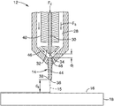
도 2는 도 1의 증착 헤드의 내부 형태를 나타내는 개략 단면도이다.
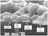
도 3은 증착 헤드에 유동 콘이 없는(좌측) 그리고 유동 콘이 있는(우측) 유리 상에 증착된 동 라인들의 이미지를 나타낸다.
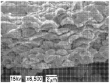
도 4a-4c는 각각 50 psi 압력, 80 psi 압력, 및 110 psi 압력으로 실리콘 상에 증착된 동 라인들의 횡단면 SEM 이미지들을 나타낸다.
도 5는 본 발명에 따른 동으로 채워진 150 ㎛ 직경 비아 홀의 SEM 이미지이다.
도 6은 본 발명에 따른 알루미늄 동으로 채워진 150, 100 및 75 ㎛ 비아 홀의 SEM 이미지이다.
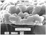
도 7a 및 7b는 바람직한 그리고 바람직하지 않은 마이크로구조를 나타내는 실리콘 상에 증착된 알루미늄 라인들의 고해상도 횡단면 SEM 이미지들을 나타낸다.
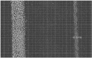
도 8a 및 8b는 종래의 노즐을 빠져나가는 2 ㎛ 입자 궤적의 이미지들을 나타낸다.
도 9는 본 발명에 따른 노즐 구성을 나타낸다.
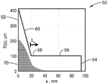
도 10은 400 ㎛ 입구 및 100 ㎛ 출구를 갖는 합류(수렴)의 일정 반경 노즐을 통해 유동되는 2 ㎛ 직경의 에어로졸 입자들의 시뮬레이션을 나타낸다.
도 11은 카본-테이프(carbon-tape) 상의 실험용 에어로졸 유동을 위한 4 ㎛ 실리카 분말의 스캐닝 전자 현미경(SEM; scanning electron microscope) 이미지이다.
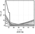
도 12는 스토크스 힘(Stokes force)만을 이용하는 이론과 비교된 선형적-합류의 200 ㎛ 노즐, 및 161 ㎛ 합류의 알루미나(세라믹) 노즐에 대한 노즐 출구로부터의 거리 대 빔 폭의 그래프이다.
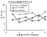
도 13은 길이 11.84 mm, 17 mm, 및 30 mm의 200 ㎛ 직선 섹션을 갖는 161 ㎛ 합류의 알루미나(세라믹) 노즐에 대한 노즐 출구로부터의 거리 대 빔 폭의 그래프이다.
| 기판 재료 | 주석 | 알루미늄 | 동 |
| 유리 | 예 | 예 | 예 |
| 실리콘 | 예 | 예 | 예 |
| BT | 예 | 예 | 아니오 |
| PEEK | 아니오 | 예 | 예 |
| 캡톤(Kapton) | 예 | 예 | 아니오 |
| 테플론(Teflon) | 아니오 | 예 | 예 |
| PES | 아니오 | 예 | 예 |
| LCP | 아니오 | 예 | 예 |
| 테슬린(Teslin) | 아니오 | 아니오 | 예 |
| FR4 | 아니오 | 예 | 아니오 |
| 마일라(Mylar) | 아니오 | 예 | 예 |
Claims (50)
- 기판 상에 고체 입자들의 증착을 위해 구성된 마이크로 콜드 스프레이 직접-기록 시스템으로서,
증착 헤드;
상기 증착 헤드의 입력부에 연결되고, 고체 입자들을 포함하는 분무형 전구체 재료를 이송하도록 구성된 캐리어 가스 공급 라인; 및
상기 증착 헤드에 연결되고, 상기 증착 헤드에 가속 가스를 이송하도록 구성된 가속 가스 공급 라인을 포함하며,
상기 증착 헤드는 증착 헤드의 출력부에 노즐을 포함하고,
상기 노즐은 입구 개구 및 출구 개구를 갖추며,
상기 가속 가스는 기판 상에 정형 형태를 생성하기 위해 기판에 충돌됨에 따라 고체 입자들이 변형되도록 고속의 에어로졸 빔으로서 노즐의 출구 개구 밖으로 캐리어 가스를 몰아내도록 이루어진, 마이크로 콜드 스프레이 직접-기록 시스템. - 청구항 1에 있어서,
상기 증착 헤드는 적어도 상기 증착 헤드의 길이를 따라 입력부로부터 캐리어 가스를 전송하도록 구성된 제1채널을 포함하고,
상기 제1채널은 노즐의 입구 개구와 출구 포트간 갭을 형성하도록 상기 노즐의 입구 개구로부터 공간 이격된 출구 포트를 갖추며,
상기 증착 헤드는 캐리어 가스와 통합시키기 위해 상기 갭으로 가속 가스를 전송하도록 구성된 제2채널을 포함하는, 마이크로 콜드 스프레이 직접-기록 시스템. - 청구항 1에 있어서,
상기 입자들은 금속 성분을 포함하며,
상기 정형 형태는 기판 상에 전도성 형태를 포함하는, 마이크로 콜드 스프레이 직접-기록 시스템. - 청구항 3에 있어서,
상기 형태는 1 ㎛ 내지 500 ㎛ 범위의 폭을 갖는 라인을 포함하는, 마이크로 콜드 스프레이 직접-기록 시스템. - 청구항 4에 있어서,
상기 형태는 5 ㎛와 100 ㎛ 범위의 폭을 갖는 라인을 포함하는, 마이크로 콜드 스프레이 직접-기록 시스템. - 청구항 5에 있어서,
상기 형태는 10 ㎛와 50 ㎛ 범위의 폭을 갖는 라인을 포함하는, 마이크로 콜드 스프레이 직접-기록 시스템. - 청구항 1에 있어서,
출구 개구에서 에어로졸 빔은 200 m/s와 1000 m/s 사이 범위의 속도를 갖는, 마이크로 콜드 스프레이 직접-기록 시스템. - 청구항 2에 있어서,
제1채널은 노즐과 거의 동심으로 위치되고,
제2채널은 캐리어 가스에 대해 비스듬히 갭으로 가속 가스를 전송하도록 구성된, 마이크로 콜드 스프레이 직접-기록 시스템. - 청구항 8에 있어서,
제2채널은 갭으로 이끌어지는 원뿔형 채널을 형성하고,
제1채널의 출구 포트는 상기 원뿔형 채널의 정점에서 끝나는, 마이크로 콜드 스프레이 직접-기록 시스템. - 청구항 2에 있어서,
노즐은 테이퍼진 합류 보어를 포함하고,
상기 노즐의 입구 개구는 출구 개구의 직경보다 큰, 마이크로 콜드 스프레이 직접-기록 시스템. - 청구항 10에 있어서,
노즐은 상기 노즐의 입구 개구로부터 이어지는 테이퍼진 합류 보어를 포함하고,
상기 테이퍼진 합류 보어는 상기 노즐의 출구 개구로 이어지는 거의 일정한 직경의 보어가 뒤따르는, 마이크로 콜드 스프레이 직접-기록 시스템. - 청구항 10에 있어서,
에어로졸 빔의 직경은 보어의 출구 개구의 직경보다 상당히 작은 직경으로 포커스되는, 마이크로 콜드 스프레이 직접-기록 시스템. - 청구항 10에 있어서,
에어로졸 빔은 실질적으로 노즐의 출구 개구를 빠져나감에 따라 시준되는, 마이크로 콜드 스프레이 직접-기록 시스템. - 청구항 13에 있어서,
에어로졸 빔은 노즐의 출구 개구를 빠져나가기 전에 보어의 형태가 되는, 마이크로 콜드 스프레이 직접-기록 시스템. - 청구항 2에 있어서,
제1 및 제2채널에 인접하여 배치된 가열 요소를 더 포함하며,
상기 가열 요소는 노즐을 통해 가속됨에 따라 캐리어 및 가소 가스의 온도로 물방울을 보상하기 위해 미리 결정된 온도로 캐리어 및 가속 가스를 가열하도록 구성되는, 마이크로 콜드 스프레이 직접-기록 시스템. - 기판 상에 고체 입자들의 증착을 위해 구성된 마이크로 콜드 스프레이 직접-기록 증착 헤드로서,
고체 입자들을 포함한 분무형 전구체 재료를 포함하는 캐리어 가스를 받아들이기 위한 제1입력부;
가속 가스를 받아들이기 위한 제2입력부; 및
증착 헤드의 출력부의 노즐를 포함하며,
상기 노즐은 입구 개구 및 출구 개구를 갖추고,
상기 가속 가스는 기판 상에 정형 형태를 생성하기 위해 기판에 충돌됨에 따라 고체 입자들이 변형되도록 고속의 에어로졸 빔으로서 노즐의 출구 개구 밖으로 캐리어 가스를 몰아내도록 이루어진, 마이크로 콜드 스프레이 직접-기록 증착 헤드. - 청구항 16에 있어서,
적어도 상기 증착 헤드의 길이를 따라 입력부로부터 캐리어 가스를 전송하도록 구성되고, 노즐의 입구 개구와 출구 포트간 갭을 형성하도록 상기 노즐의 입구 개구로부터 공간 이격된 출구 포트를 갖춘 제1채널; 및
캐리어 가스와 통합시키기 위해 상기 갭으로 가속 가스를 전송하도록 구성된 제2채널을 더 포함하는, 마이크로 콜드 스프레이 직접-기록 증착 헤드. - 청구항 16에 있어서,
상기 입자들은 금속 성분을 포함하며,
상기 정형 형태는 기판 상에 전도성 형태를 포함하는, 마이크로 콜드 스프레이 직접-기록 증착 헤드. - 청구항 18에 있어서,
상기 형태는 1 ㎛ 내지 200 ㎛ 범위의 폭을 갖는 라인을 포함하는, 마이크로 콜드 스프레이 직접-기록 증착 헤드. - 청구항 19에 있어서,
상기 형태는 5 ㎛와 100 ㎛ 범위의 폭을 갖는 라인을 포함하는, 마이크로 콜드 스프레이 직접-기록 증착 헤드. - 청구항 20에 있어서,
상기 형태는 10 ㎛와 50 ㎛ 범위의 폭을 갖는 라인을 포함하는, 마이크로 콜드 스프레이 직접-기록 증착 헤드. - 청구항 16에 있어서,
출구 개구에서 에어로졸 빔은 200 m/s와 1000 m/s 사이 범위의 속도를 갖는, 마이크로 콜드 스프레이 직접-기록 증착 헤드. - 청구항 22에 있어서,
제1채널은 노즐과 거의 동심으로 위치되고,
제2채널은 캐리어 가스에 대해 비스듬히 갭으로 가속 가스를 전송하도록 구성된, 마이크로 콜드 스프레이 직접-기록 증착 헤드. - 청구항 23에 있어서,
제2채널은 갭으로 이끌어지는 원뿔형 채널을 형성하고,
제1채널의 출구 포트는 상기 원뿔형 채널의 정점에서 끝나는, 마이크로 콜드 스프레이 직접-기록 증착 헤드. - 청구항 17에 있어서,
노즐은 테이퍼진 합류 보어를 포함하고,
상기 노즐의 입구 개구는 출구 개구의 직경보다 큰, 마이크로 콜드 스프레이 직접-기록 증착 헤드. - 청구항 25에 있어서,
노즐은 상기 노즐의 입구 개구로부터 이어지는 테이퍼진 합류 보어를 포함하고,
상기 테이퍼진 합류 보어는 상기 노즐의 출구 개구로 이어지는 거의 일정한 직경의 보어가 뒤따르는, 마이크로 콜드 스프레이 직접-기록 증착 헤드. - 청구항 25에 있어서,
에어로졸 빔은 보어의 출구 개구의 직경보다 상당히 작은 직경으로 포커스되는, 마이크로 콜드 스프레이 직접-기록 증착 헤드. - 청구항 25에 있어서,
에어로졸 빔은 실질적으로 노즐의 출구 개구를 빠져나감에 따라 시준되는, 마이크로 콜드 스프레이 직접-기록 증착 헤드. - 청구항 28에 있어서,
에어로졸 빔은 노즐의 출구 개구를 빠져나가기 전에 보어의 형태가 되는, 마이크로 콜드 스프레이 직접-기록 증착 헤드. - 청구항 17에 있어서,
제1 및 제2채널에 인접하여 배치된 가열 요소를 더 포함하며,
상기 가열 요소는 노즐을 통해 가속됨에 따라 캐리어 및 가소 가스의 온도로 물방울을 보상하기 위해 미리 결정된 온도로 캐리어 및 가속 가스를 가열하도록 구성되는, 마이크로 콜드 스프레이 직접-기록 증착 헤드. - 청구항 16에 있어서,
상기 정형 형태는 변형가능 고체를 포함하는, 마이크로 콜드 스프레이 직접-기록 증착 헤드. - 청구항 16에 있어서,
상기 정형 형태는 폴리머를 포함하는, 마이크로 콜드 스프레이 직접-기록 증착 헤드. - 청구항 32에 있어서,
상기 폴리머는 절연체로서 작용하는, 마이크로 콜드 스프레이 직접-기록 증착 헤드. - 인쇄 회로 애플리케이션을 위한 기판 상에 고체 금속 입자들의 분무형 분말을 증착하기 위한 방법으로서,
정형 형태를 형성하기 위해 기판 상에 분무형 분말을 콜드 스프레이하는 단계를 포함하며,
상기 정형 형태의 길이 및 폭의 치수 중 적어도 하나는 500 μ 이하인, 기판 상에 고체 금속 입자들의 분무형 분말을 증착하기 위한 방법. - 청구항 34에 있어서,
상기 정형 형태는 5 ㎛와 100 ㎛ 범위의 라인 폭을 포함하는, 기판 상에 고체 금속 입자들의 분무형 분말을 증착하기 위한 방법. - 청구항 35에 있어서,
상기 정형 형태는 10 ㎛와 50 ㎛ 범위의 라인 폭을 포함하는, 기판 상에 고체 금속 입자들의 분무형 분말을 증착하기 위한 방법. - 청구항 34에 있어서,
고체 금속 분말은 기판 상에 정형 형태를 생성하기 위해 기판에 충돌됨에 따라 고체 입자들이 변형되도록 고속 에어로졸 빔으로서 증착되는, 기판 상에 고체 금속 입자들의 분무형 분말을 증착하기 위한 방법. - 청구항 37에 있어서,
출구 개구에서 에어로졸 빔은 200 m/s와 1000 m/s 사이 범위의 속도를 갖는, 기판 상에 고체 금속 입자들의 분무형 분말을 증착하기 위한 방법. - 청구항 34에 있어서,
분무형 분말을 콜드 스프레이하는 단계는;
상기 분무형 분말을 이송하는 캐리어 가스를 증착 헤드로 투입하는 단계;
금속 입자들을 가속하기 위해 증착 헤드로 가속 가스를 투입하는 단계; 및
고속 에어로졸 빔을 형성하기 위해 노즐의 출구 개구 밖으로 캐리어 가스를 몰아내도록 가속 가스를 캐리어 가수와 통합시키는 단계를 포함하며,
상기 증착 헤드는 이 증착 헤드의 출럭부에 노즐을 포함하고,
상기 노즐은 입구 개구 및 출구 개구를 갖춘, 기판 상에 고체 금속 입자들의 분무형 분말을 증착하기 위한 방법. - 청구항 39에 있어서,
노즐을 통과해 감에 따라 가속 및 캐리어 가스의 온도로 물방울을 보상하기 위해 미리 결정된 온도로 증착 헤드를 가열하는 단계를 더 포함하는, 기판 상에 고체 금속 입자들의 분무형 분말을 증착하기 위한 방법. - 청구항 39에 있어서,
증착 헤드는 적어도 상기 증착 헤드의 길이를 따라 입력부로부터 캐리어 가스를 전송하도록 구성된 제1채널을 포함하고,
상기 제1채널은 노즐의 입구 개구와 출구 포트간 갭을 형성하도록 상기 노즐의 입구 개구로부터 공간 이격된 출구 포트를 갖추며,
상기 증착 헤드는 캐리어 가스와 통합시키기 위해 상기 갭에 가속 가스를 전송하도록 구성된 제2채널을 포함하는, 기판 상에 고체 금속 입자들의 분무형 분말을 증착하기 위한 방법. - 청구항 37에 있어서,
정형 형태는 기판 상에 전도성 형태를 포함하는, 기판 상에 고체 금속 입자들의 분무형 분말을 증착하기 위한 방법. - 청구항 41에 있어서,
제1채널은 노즐과 거의 동심으로 위치되고,
제2채널은 캐리어 가스에 대해 비스듬히 갭으로 가속 가스를 전송하도록 구성된, 기판 상에 고체 금속 입자들의 분무형 분말을 증착하기 위한 방법. - 청구항 43에 있어서,
제2채널은 갭으로 이끌어지는 원뿔형 채널을 형성하고,
제1채널의 출구 포트는 상기 원뿔형 채널의 정점에서 끝나는, 기판 상에 고체 금속 입자들의 분무형 분말을 증착하기 위한 방법. - 청구항 39에 있어서,
에어로졸 빔은 보어의 출구 개구의 직경보다 상당히 작은 직경으로 포커스되는, 기판 상에 고체 금속 입자들의 분무형 분말을 증착하기 위한 방법. - 청구항 39에 있어서,
에어로졸 빔은 실질적으로 노즐의 출구 개구를 빠져나감에 따라 시준되는, 기판 상에 고체 금속 입자들의 분무형 분말을 증착하기 위한 방법. - 청구항 46에 있어서,
에어로졸 빔은 노즐의 출구 개구를 빠져나가기 전에 보어의 형태가 되는, 기판 상에 고체 금속 입자들의 분무형 분말을 증착하기 위한 방법. - 청구항 34에 있어서,
정형 형태는 변형가능 고체를 포함하는, 기판 상에 고체 금속 입자들의 분무형 분말을 증착하기 위한 방법. - 청구항 34에 있어서,
정형 형태는 폴리머를 포함하는, 기판 상에 고체 금속 입자들의 분무형 분말을 증착하기 위한 방법. - 청구항 49에 있어서,
상기 폴리머는 절연체로서 작용하는, 기판 상에 고체 금속 입자들의 분무형 분말을 증착하기 위한 방법.
Applications Claiming Priority (5)
| Application Number | Priority Date | Filing Date | Title |
|---|---|---|---|
| US201261591365P | 2012-01-27 | 2012-01-27 | |
| US61/591,365 | 2012-01-27 | ||
| US201261691112P | 2012-08-20 | 2012-08-20 | |
| US61/691,112 | 2012-08-20 | ||
| PCT/US2013/023320 WO2013158178A2 (en) | 2012-01-27 | 2013-01-25 | Micro cold spray direct write systems and methods for printed micro electronics |
Publications (1)
| Publication Number | Publication Date |
|---|---|
| KR20140127802A true KR20140127802A (ko) | 2014-11-04 |
Family
ID=49384200
Family Applications (1)
| Application Number | Title | Priority Date | Filing Date |
|---|---|---|---|
| KR1020147018804A Ceased KR20140127802A (ko) | 2012-01-27 | 2013-01-25 | 인쇄 마이크로 전자를 위한 마이크로 콜드 스프레이 직접 기록 시스템 및 방법 |
Country Status (4)
| Country | Link |
|---|---|
| US (1) | US20140370203A1 (ko) |
| JP (1) | JP2015511270A (ko) |
| KR (1) | KR20140127802A (ko) |
| WO (1) | WO2013158178A2 (ko) |
Cited By (1)
| Publication number | Priority date | Publication date | Assignee | Title |
|---|---|---|---|---|
| KR102330271B1 (ko) * | 2021-05-31 | 2021-11-23 | 허수영 | 공압 디스펜서의 액체 토출량 보정 시스템 |
Families Citing this family (21)
| Publication number | Priority date | Publication date | Assignee | Title |
|---|---|---|---|---|
| WO2014125591A1 (ja) * | 2013-02-14 | 2014-08-21 | 株式会社島津製作所 | 微細パターニング用表面化学処理装置 |
| US10933636B2 (en) * | 2013-12-06 | 2021-03-02 | Palo Alto Research Center Incorporated | Print head design for ballistic aerosol marking with smooth particulate injection from an array of inlets into a matching array of microchannels |
| JP5889938B2 (ja) * | 2014-03-06 | 2016-03-22 | 日本発條株式会社 | 積層体および積層体の製造方法 |
| CN103831182B (zh) * | 2014-03-20 | 2016-03-02 | 浙江明泉工业涂装有限公司 | 立式型材静电喷涂涂装设备 |
| US10440829B2 (en) * | 2014-07-03 | 2019-10-08 | United Technologies Corporation | Heating circuit assembly and method of manufacture |
| RU2588921C2 (ru) * | 2014-09-25 | 2016-07-10 | Общество С Ограниченной Ответственностью "Ласком" | Способ формирования токоведущей шины на низкоэмиссионной поверхности стекла |
| JP6065892B2 (ja) * | 2014-10-30 | 2017-01-25 | トヨタ自動車株式会社 | レーザクラッド加工装置およびその運転方法 |
| DE102016001810A1 (de) | 2016-02-17 | 2017-08-17 | Häusermann GmbH | Verfahren zur Herstellung einer Leiterplatte mit verstärkter Kupferstruktur |
| US20170336431A1 (en) * | 2016-05-19 | 2017-11-23 | Purdue Research Foundation | System and method for measuring exhaust flow velocity of supersonic nozzles |
| CN105944632B (zh) * | 2016-07-11 | 2017-09-26 | 中国环境科学研究院 | 一种防止低流动性药物结块的粉末气溶胶发生器 |
| US10029476B2 (en) | 2016-09-30 | 2018-07-24 | Hamilton Sundstrand Corporation | Laser enhancements of micro cold spray printed powder |
| US11617610B2 (en) * | 2018-04-26 | 2023-04-04 | Us Patent Innovations Llc | System and method for micro-sized cold atmospheric plasma treatment |
| US11136480B2 (en) * | 2018-08-01 | 2021-10-05 | The Boeing Company | Thermal spray plastic coating for edge sealing and fillet sealing |
| US20200040214A1 (en) | 2018-08-01 | 2020-02-06 | The Boeing Company | Thermoplastic Coating Formulations For High-Velocity Sprayer Application and Methods For Applying Same |
| US11591103B2 (en) | 2019-03-28 | 2023-02-28 | The Boeing Company | Multi-layer thermoplastic spray coating system for high performance sealing on airplanes |
| EP3789516A1 (de) * | 2019-09-09 | 2021-03-10 | Siemens Aktiengesellschaft | Kaltgasspritzanlage mit einstellbarem partikelstrahl |
| DE102020103232A1 (de) | 2020-02-07 | 2021-08-12 | Fachhochschule Münster | Verfahren zum Aufbringen von Partikel auf ein Substrat |
| JP7849787B2 (ja) * | 2020-03-31 | 2026-04-22 | 大阪瓦斯株式会社 | 成膜装置及びセラミックス膜の製造方法 |
| TWI817108B (zh) * | 2021-04-16 | 2023-10-01 | 張有諒 | 液晶高分子薄膜電氣圖樣製造方法 |
| KR102866116B1 (ko) | 2021-11-26 | 2025-09-30 | 삼성전자주식회사 | 반도체 패키지 |
| KR102786474B1 (ko) * | 2022-03-31 | 2025-03-27 | 참엔지니어링(주) | 노즐형 증착장치 |
Family Cites Families (19)
| Publication number | Priority date | Publication date | Assignee | Title |
|---|---|---|---|---|
| JPS5980361A (ja) * | 1982-10-29 | 1984-05-09 | Chikara Hayashi | 超微粒子の膜形成法 |
| DE69016433T2 (de) * | 1990-05-19 | 1995-07-20 | Papyrin Anatolij Nikiforovic | Beschichtungsverfahren und -vorrichtung. |
| US20040197493A1 (en) * | 1998-09-30 | 2004-10-07 | Optomec Design Company | Apparatus, methods and precision spray processes for direct write and maskless mesoscale material deposition |
| US6258402B1 (en) * | 1999-10-12 | 2001-07-10 | Nakhleh Hussary | Method for repairing spray-formed steel tooling |
| RU2213805C2 (ru) * | 2001-10-23 | 2003-10-10 | Крыса Валерий Корнеевич | Способ нанесения покрытий из порошковых материалов и устройство для его осуществления |
| EP1572377B1 (en) * | 2002-12-17 | 2008-05-28 | The Research Foundation Of State University Of New York | Direct writing of metallic conductor patterns on insulating surfaces |
| JP4044515B2 (ja) * | 2003-11-28 | 2008-02-06 | 富士通株式会社 | エアロゾルデポジッション成膜装置 |
| US20060121187A1 (en) * | 2004-12-03 | 2006-06-08 | Haynes Jeffrey D | Vacuum cold spray process |
| US7938341B2 (en) * | 2004-12-13 | 2011-05-10 | Optomec Design Company | Miniature aerosol jet and aerosol jet array |
| CA2571099C (en) * | 2005-12-21 | 2015-05-05 | Sulzer Metco (Us) Inc. | Hybrid plasma-cold spray method and apparatus |
| US20090053507A1 (en) * | 2007-08-17 | 2009-02-26 | Ndsu Research Foundation | Convergent-divergent-convergent nozzle focusing of aerosol particles for micron-scale direct writing |
| JP5130991B2 (ja) * | 2008-03-27 | 2013-01-30 | 株式会社Ihi | コールドスプレー方法、コールドスプレー装置 |
| US8020509B2 (en) * | 2009-01-08 | 2011-09-20 | General Electric Company | Apparatus, systems, and methods involving cold spray coating |
| JP2010229533A (ja) * | 2009-03-30 | 2010-10-14 | Brother Ind Ltd | 成膜方法 |
| BR112012013498B1 (pt) * | 2009-12-04 | 2020-08-18 | The Regents Of The University Of Michigan | Montagem de bico de borrifo a frio e método de cobertura por borrifo a frio |
| US8389066B2 (en) * | 2010-04-13 | 2013-03-05 | Vln Advanced Technologies, Inc. | Apparatus and method for prepping a surface using a coating particle entrained in a pulsed waterjet or airjet |
| JP2011240314A (ja) * | 2010-05-21 | 2011-12-01 | Kobe Steel Ltd | コールドスプレー装置 |
| KR101171535B1 (ko) * | 2010-07-09 | 2012-08-07 | 아주대학교산학협력단 | 박막의 부착력 향상을 위한 전처리 장치 및 전처리 방법 |
| US8544408B2 (en) * | 2011-03-23 | 2013-10-01 | Kevin Wayne Ewers | System for applying metal particulate with hot pressurized air using a venturi chamber and a helical channel |
-
2013
- 2013-01-25 WO PCT/US2013/023320 patent/WO2013158178A2/en not_active Ceased
- 2013-01-25 KR KR1020147018804A patent/KR20140127802A/ko not_active Ceased
- 2013-01-25 JP JP2014554896A patent/JP2015511270A/ja active Pending
-
2014
- 2014-07-16 US US14/333,124 patent/US20140370203A1/en not_active Abandoned
Cited By (1)
| Publication number | Priority date | Publication date | Assignee | Title |
|---|---|---|---|---|
| KR102330271B1 (ko) * | 2021-05-31 | 2021-11-23 | 허수영 | 공압 디스펜서의 액체 토출량 보정 시스템 |
Also Published As
| Publication number | Publication date |
|---|---|
| US20140370203A1 (en) | 2014-12-18 |
| WO2013158178A2 (en) | 2013-10-24 |
| WO2013158178A3 (en) | 2014-01-30 |
| JP2015511270A (ja) | 2015-04-16 |
Similar Documents
| Publication | Publication Date | Title |
|---|---|---|
| KR20140127802A (ko) | 인쇄 마이크로 전자를 위한 마이크로 콜드 스프레이 직접 기록 시스템 및 방법 | |
| US7674671B2 (en) | Aerodynamic jetting of aerosolized fluids for fabrication of passive structures | |
| KR101160701B1 (ko) | 기판 및 그 제조방법 | |
| US7108894B2 (en) | Direct Write™ System | |
| Zürcher et al. | Nanoparticle assembly and sintering towards all-copper flip chip interconnects | |
| US20050156991A1 (en) | Maskless direct write of copper using an annular aerosol jet | |
| US20070019028A1 (en) | Laser processing for heat-sensitive mesoscale deposition of oxygen-sensitive materials | |
| Laurila et al. | Combination of E-jet and inkjet printing for additive fabrication of multilayer high-density RDL of silicon interposer | |
| JP6132293B2 (ja) | 基材上に形成した構造体、構造体の製造方法および線パターン | |
| Lall et al. | Effect of Process Parameters on Aerosol Jet Printing of Multi-Layer Circuitry | |
| EP1845382B1 (en) | Probe card and method for manufacturing same | |
| US20090053507A1 (en) | Convergent-divergent-convergent nozzle focusing of aerosol particles for micron-scale direct writing | |
| Renn et al. | Aerosol Jet® Printing of Conductive Epoxy for 3D Packaging | |
| Felba et al. | Materials and technology for conductive microstructures | |
| Soukup et al. | A comparison of the interdigital electrodes prepared by aerosol jet printing and lift-off technique | |
| Pandiya et al. | Comparison of Sintering Methodologies for 3D Printed High-Density Interconnects (2.3 L/S) on Organic Substrates for High-Performance Computing Applications | |
| Hedges et al. | Aerosol-Jet Printing for 3-D Interconnects, Flexible Substrates and Embedded Passives | |
| Lee et al. | Advanced inkjet-based 3D ramp interconnection via dielectric ramp fabrication for multilayered devices | |
| Lall et al. | Process Development for Additive Fabrication of Z-Axis Interconnects In Multilayer Circuits | |
| Hurley | Electrospray Printing of Polymeric Films onto Substrates with Non-Homogenous Electrical Properties | |
| Wits et al. | Inkjet Printing of 3D Metallic Silver Complex Microstructures | |
| Park et al. | Tae Geun Kim 5 Email tgkim1@ korea. ac. kr Byung Chul Lee 1, 6, 7✉ Email bclee@ kist. re. kr | |
| Renn | Aerosol-based direct writing of interconnects | |
| Jäger et al. | Flexible and Printed Electronics | |
| WO2023069739A1 (en) | Microchannel printing |
Legal Events
| Date | Code | Title | Description |
|---|---|---|---|
| PA0105 | International application |
Patent event date: 20140707 Patent event code: PA01051R01D Comment text: International Patent Application |
|
| PG1501 | Laying open of application | ||
| A201 | Request for examination | ||
| PA0201 | Request for examination |
Patent event code: PA02012R01D Patent event date: 20180117 Comment text: Request for Examination of Application |
|
| E902 | Notification of reason for refusal | ||
| PE0902 | Notice of grounds for rejection |
Comment text: Notification of reason for refusal Patent event date: 20190611 Patent event code: PE09021S01D |
|
| E601 | Decision to refuse application | ||
| PE0601 | Decision on rejection of patent |
Patent event date: 20190819 Comment text: Decision to Refuse Application Patent event code: PE06012S01D Patent event date: 20190611 Comment text: Notification of reason for refusal Patent event code: PE06011S01I |