KR20140133963A - 액정 표시 장치 - Google Patents
액정 표시 장치 Download PDFInfo
- Publication number
- KR20140133963A KR20140133963A KR1020147030621A KR20147030621A KR20140133963A KR 20140133963 A KR20140133963 A KR 20140133963A KR 1020147030621 A KR1020147030621 A KR 1020147030621A KR 20147030621 A KR20147030621 A KR 20147030621A KR 20140133963 A KR20140133963 A KR 20140133963A
- Authority
- KR
- South Korea
- Prior art keywords
- common electrode
- sub
- pixel electrode
- main
- electrode
- Prior art date
- Legal status (The legal status is an assumption and is not a legal conclusion. Google has not performed a legal analysis and makes no representation as to the accuracy of the status listed.)
- Ceased
Links
- 239000004973 liquid crystal related substance Substances 0.000 title claims abstract description 132
- 239000000463 material Substances 0.000 claims abstract description 14
- 230000001747 exhibiting effect Effects 0.000 claims abstract description 9
- 239000000758 substrate Substances 0.000 claims description 180
- 239000003990 capacitor Substances 0.000 claims description 47
- 230000005684 electric field Effects 0.000 claims description 30
- 238000000034 method Methods 0.000 claims description 15
- 230000008878 coupling Effects 0.000 claims description 3
- 238000010168 coupling process Methods 0.000 claims description 3
- 238000005859 coupling reaction Methods 0.000 claims description 3
- 230000007246 mechanism Effects 0.000 claims description 2
- 239000007921 spray Substances 0.000 claims description 2
- 239000010408 film Substances 0.000 description 84
- 239000010410 layer Substances 0.000 description 36
- 239000011229 interlayer Substances 0.000 description 29
- 101100063431 Arabidopsis thaliana DIM gene Proteins 0.000 description 18
- 101100382340 Arabidopsis thaliana CAM2 gene Proteins 0.000 description 16
- 101100494530 Brassica oleracea var. botrytis CAL-A gene Proteins 0.000 description 16
- 101100165913 Brassica oleracea var. italica CAL gene Proteins 0.000 description 16
- 101150118283 CAL1 gene Proteins 0.000 description 16
- 101100029577 Saccharomyces cerevisiae (strain ATCC 204508 / S288c) CDC43 gene Proteins 0.000 description 16
- 101100439683 Saccharomyces cerevisiae (strain ATCC 204508 / S288c) CHS3 gene Proteins 0.000 description 16
- 101150014174 calm gene Proteins 0.000 description 16
- 102100024633 Carbonic anhydrase 2 Human genes 0.000 description 15
- 101000760643 Homo sapiens Carbonic anhydrase 2 Proteins 0.000 description 15
- 102100021849 Calretinin Human genes 0.000 description 14
- 101000898072 Homo sapiens Calretinin Proteins 0.000 description 14
- 230000003287 optical effect Effects 0.000 description 8
- 239000004065 semiconductor Substances 0.000 description 7
- 239000004020 conductor Substances 0.000 description 5
- 239000011159 matrix material Substances 0.000 description 5
- 230000010287 polarization Effects 0.000 description 5
- 230000008569 process Effects 0.000 description 4
- 230000000694 effects Effects 0.000 description 3
- 239000010409 thin film Substances 0.000 description 3
- 238000002834 transmittance Methods 0.000 description 3
- 239000000853 adhesive Substances 0.000 description 2
- 230000001070 adhesive effect Effects 0.000 description 2
- XAGFODPZIPBFFR-UHFFFAOYSA-N aluminium Chemical compound [Al] XAGFODPZIPBFFR-UHFFFAOYSA-N 0.000 description 2
- 229910052782 aluminium Inorganic materials 0.000 description 2
- 230000008901 benefit Effects 0.000 description 2
- 230000008859 change Effects 0.000 description 2
- 230000002950 deficient Effects 0.000 description 2
- 239000011521 glass Substances 0.000 description 2
- 229920005989 resin Polymers 0.000 description 2
- 239000011347 resin Substances 0.000 description 2
- ZOKXTWBITQBERF-UHFFFAOYSA-N Molybdenum Chemical compound [Mo] ZOKXTWBITQBERF-UHFFFAOYSA-N 0.000 description 1
- 229910052581 Si3N4 Inorganic materials 0.000 description 1
- VYPSYNLAJGMNEJ-UHFFFAOYSA-N Silicium dioxide Chemical compound O=[Si]=O VYPSYNLAJGMNEJ-UHFFFAOYSA-N 0.000 description 1
- RTAQQCXQSZGOHL-UHFFFAOYSA-N Titanium Chemical compound [Ti] RTAQQCXQSZGOHL-UHFFFAOYSA-N 0.000 description 1
- 230000004075 alteration Effects 0.000 description 1
- 229910021417 amorphous silicon Inorganic materials 0.000 description 1
- 230000008602 contraction Effects 0.000 description 1
- 230000006866 deterioration Effects 0.000 description 1
- 238000010586 diagram Methods 0.000 description 1
- AMGQUBHHOARCQH-UHFFFAOYSA-N indium;oxotin Chemical compound [In].[Sn]=O AMGQUBHHOARCQH-UHFFFAOYSA-N 0.000 description 1
- 229910010272 inorganic material Inorganic materials 0.000 description 1
- 239000011147 inorganic material Substances 0.000 description 1
- 230000004048 modification Effects 0.000 description 1
- 238000012986 modification Methods 0.000 description 1
- 229910052750 molybdenum Inorganic materials 0.000 description 1
- 239000011733 molybdenum Substances 0.000 description 1
- 239000011368 organic material Substances 0.000 description 1
- 238000005192 partition Methods 0.000 description 1
- 229910021420 polycrystalline silicon Inorganic materials 0.000 description 1
- 229920005591 polysilicon Polymers 0.000 description 1
- 239000003566 sealing material Substances 0.000 description 1
- HQVNEWCFYHHQES-UHFFFAOYSA-N silicon nitride Chemical compound N12[Si]34N5[Si]62N3[Si]51N64 HQVNEWCFYHHQES-UHFFFAOYSA-N 0.000 description 1
- 229910052814 silicon oxide Inorganic materials 0.000 description 1
- 229910052709 silver Inorganic materials 0.000 description 1
- 239000004332 silver Substances 0.000 description 1
- 125000006850 spacer group Chemical group 0.000 description 1
- 238000006467 substitution reaction Methods 0.000 description 1
- 229920001187 thermosetting polymer Polymers 0.000 description 1
- 239000010936 titanium Substances 0.000 description 1
- 229910052719 titanium Inorganic materials 0.000 description 1
- WFKWXMTUELFFGS-UHFFFAOYSA-N tungsten Chemical compound [W] WFKWXMTUELFFGS-UHFFFAOYSA-N 0.000 description 1
- 229910052721 tungsten Inorganic materials 0.000 description 1
- 239000010937 tungsten Substances 0.000 description 1
- YVTHLONGBIQYBO-UHFFFAOYSA-N zinc indium(3+) oxygen(2-) Chemical compound [O--].[Zn++].[In+3] YVTHLONGBIQYBO-UHFFFAOYSA-N 0.000 description 1
Images



Classifications
-
- G—PHYSICS
- G09—EDUCATION; CRYPTOGRAPHY; DISPLAY; ADVERTISING; SEALS
- G09G—ARRANGEMENTS OR CIRCUITS FOR CONTROL OF INDICATING DEVICES USING STATIC MEANS TO PRESENT VARIABLE INFORMATION
- G09G3/00—Control arrangements or circuits, of interest only in connection with visual indicators other than cathode-ray tubes
- G09G3/20—Control arrangements or circuits, of interest only in connection with visual indicators other than cathode-ray tubes for presentation of an assembly of a number of characters, e.g. a page, by composing the assembly by combination of individual elements arranged in a matrix no fixed position being assigned to or needed to be assigned to the individual characters or partial characters
- G09G3/34—Control arrangements or circuits, of interest only in connection with visual indicators other than cathode-ray tubes for presentation of an assembly of a number of characters, e.g. a page, by composing the assembly by combination of individual elements arranged in a matrix no fixed position being assigned to or needed to be assigned to the individual characters or partial characters by control of light from an independent source
- G09G3/36—Control arrangements or circuits, of interest only in connection with visual indicators other than cathode-ray tubes for presentation of an assembly of a number of characters, e.g. a page, by composing the assembly by combination of individual elements arranged in a matrix no fixed position being assigned to or needed to be assigned to the individual characters or partial characters by control of light from an independent source using liquid crystals
- G09G3/3611—Control of matrices with row and column drivers
-
- G—PHYSICS
- G02—OPTICS
- G02F—OPTICAL DEVICES OR ARRANGEMENTS FOR THE CONTROL OF LIGHT BY MODIFICATION OF THE OPTICAL PROPERTIES OF THE MEDIA OF THE ELEMENTS INVOLVED THEREIN; NON-LINEAR OPTICS; FREQUENCY-CHANGING OF LIGHT; OPTICAL LOGIC ELEMENTS; OPTICAL ANALOGUE/DIGITAL CONVERTERS
- G02F1/00—Devices or arrangements for the control of the intensity, colour, phase, polarisation or direction of light arriving from an independent light source, e.g. switching, gating or modulating; Non-linear optics
- G02F1/01—Devices or arrangements for the control of the intensity, colour, phase, polarisation or direction of light arriving from an independent light source, e.g. switching, gating or modulating; Non-linear optics for the control of the intensity, phase, polarisation or colour
- G02F1/13—Devices or arrangements for the control of the intensity, colour, phase, polarisation or direction of light arriving from an independent light source, e.g. switching, gating or modulating; Non-linear optics for the control of the intensity, phase, polarisation or colour based on liquid crystals, e.g. single liquid crystal display cells
- G02F1/133—Constructional arrangements; Operation of liquid crystal cells; Circuit arrangements
- G02F1/1333—Constructional arrangements; Manufacturing methods
- G02F1/1343—Electrodes
-
- G—PHYSICS
- G02—OPTICS
- G02F—OPTICAL DEVICES OR ARRANGEMENTS FOR THE CONTROL OF LIGHT BY MODIFICATION OF THE OPTICAL PROPERTIES OF THE MEDIA OF THE ELEMENTS INVOLVED THEREIN; NON-LINEAR OPTICS; FREQUENCY-CHANGING OF LIGHT; OPTICAL LOGIC ELEMENTS; OPTICAL ANALOGUE/DIGITAL CONVERTERS
- G02F1/00—Devices or arrangements for the control of the intensity, colour, phase, polarisation or direction of light arriving from an independent light source, e.g. switching, gating or modulating; Non-linear optics
- G02F1/01—Devices or arrangements for the control of the intensity, colour, phase, polarisation or direction of light arriving from an independent light source, e.g. switching, gating or modulating; Non-linear optics for the control of the intensity, phase, polarisation or colour
- G02F1/13—Devices or arrangements for the control of the intensity, colour, phase, polarisation or direction of light arriving from an independent light source, e.g. switching, gating or modulating; Non-linear optics for the control of the intensity, phase, polarisation or colour based on liquid crystals, e.g. single liquid crystal display cells
- G02F1/133—Constructional arrangements; Operation of liquid crystal cells; Circuit arrangements
- G02F1/1333—Constructional arrangements; Manufacturing methods
- G02F1/1343—Electrodes
- G02F1/134309—Electrodes characterised by their geometrical arrangement
- G02F1/134363—Electrodes characterised by their geometrical arrangement for applying an electric field parallel to the substrate, i.e. in-plane switching [IPS]
-
- G—PHYSICS
- G02—OPTICS
- G02F—OPTICAL DEVICES OR ARRANGEMENTS FOR THE CONTROL OF LIGHT BY MODIFICATION OF THE OPTICAL PROPERTIES OF THE MEDIA OF THE ELEMENTS INVOLVED THEREIN; NON-LINEAR OPTICS; FREQUENCY-CHANGING OF LIGHT; OPTICAL LOGIC ELEMENTS; OPTICAL ANALOGUE/DIGITAL CONVERTERS
- G02F1/00—Devices or arrangements for the control of the intensity, colour, phase, polarisation or direction of light arriving from an independent light source, e.g. switching, gating or modulating; Non-linear optics
- G02F1/01—Devices or arrangements for the control of the intensity, colour, phase, polarisation or direction of light arriving from an independent light source, e.g. switching, gating or modulating; Non-linear optics for the control of the intensity, phase, polarisation or colour
- G02F1/13—Devices or arrangements for the control of the intensity, colour, phase, polarisation or direction of light arriving from an independent light source, e.g. switching, gating or modulating; Non-linear optics for the control of the intensity, phase, polarisation or colour based on liquid crystals, e.g. single liquid crystal display cells
- G02F1/133—Constructional arrangements; Operation of liquid crystal cells; Circuit arrangements
- G02F1/1333—Constructional arrangements; Manufacturing methods
- G02F1/1337—Surface-induced orientation of the liquid crystal molecules, e.g. by alignment layers
-
- G—PHYSICS
- G02—OPTICS
- G02F—OPTICAL DEVICES OR ARRANGEMENTS FOR THE CONTROL OF LIGHT BY MODIFICATION OF THE OPTICAL PROPERTIES OF THE MEDIA OF THE ELEMENTS INVOLVED THEREIN; NON-LINEAR OPTICS; FREQUENCY-CHANGING OF LIGHT; OPTICAL LOGIC ELEMENTS; OPTICAL ANALOGUE/DIGITAL CONVERTERS
- G02F1/00—Devices or arrangements for the control of the intensity, colour, phase, polarisation or direction of light arriving from an independent light source, e.g. switching, gating or modulating; Non-linear optics
- G02F1/01—Devices or arrangements for the control of the intensity, colour, phase, polarisation or direction of light arriving from an independent light source, e.g. switching, gating or modulating; Non-linear optics for the control of the intensity, phase, polarisation or colour
- G02F1/13—Devices or arrangements for the control of the intensity, colour, phase, polarisation or direction of light arriving from an independent light source, e.g. switching, gating or modulating; Non-linear optics for the control of the intensity, phase, polarisation or colour based on liquid crystals, e.g. single liquid crystal display cells
- G02F1/133—Constructional arrangements; Operation of liquid crystal cells; Circuit arrangements
- G02F1/1333—Constructional arrangements; Manufacturing methods
- G02F1/1337—Surface-induced orientation of the liquid crystal molecules, e.g. by alignment layers
- G02F1/133707—Structures for producing distorted electric fields, e.g. bumps, protrusions, recesses, slits in pixel electrodes
-
- G—PHYSICS
- G02—OPTICS
- G02F—OPTICAL DEVICES OR ARRANGEMENTS FOR THE CONTROL OF LIGHT BY MODIFICATION OF THE OPTICAL PROPERTIES OF THE MEDIA OF THE ELEMENTS INVOLVED THEREIN; NON-LINEAR OPTICS; FREQUENCY-CHANGING OF LIGHT; OPTICAL LOGIC ELEMENTS; OPTICAL ANALOGUE/DIGITAL CONVERTERS
- G02F1/00—Devices or arrangements for the control of the intensity, colour, phase, polarisation or direction of light arriving from an independent light source, e.g. switching, gating or modulating; Non-linear optics
- G02F1/01—Devices or arrangements for the control of the intensity, colour, phase, polarisation or direction of light arriving from an independent light source, e.g. switching, gating or modulating; Non-linear optics for the control of the intensity, phase, polarisation or colour
- G02F1/13—Devices or arrangements for the control of the intensity, colour, phase, polarisation or direction of light arriving from an independent light source, e.g. switching, gating or modulating; Non-linear optics for the control of the intensity, phase, polarisation or colour based on liquid crystals, e.g. single liquid crystal display cells
- G02F1/133—Constructional arrangements; Operation of liquid crystal cells; Circuit arrangements
- G02F1/1333—Constructional arrangements; Manufacturing methods
- G02F1/1343—Electrodes
- G02F1/134309—Electrodes characterised by their geometrical arrangement
- G02F1/134336—Matrix
-
- G—PHYSICS
- G02—OPTICS
- G02F—OPTICAL DEVICES OR ARRANGEMENTS FOR THE CONTROL OF LIGHT BY MODIFICATION OF THE OPTICAL PROPERTIES OF THE MEDIA OF THE ELEMENTS INVOLVED THEREIN; NON-LINEAR OPTICS; FREQUENCY-CHANGING OF LIGHT; OPTICAL LOGIC ELEMENTS; OPTICAL ANALOGUE/DIGITAL CONVERTERS
- G02F1/00—Devices or arrangements for the control of the intensity, colour, phase, polarisation or direction of light arriving from an independent light source, e.g. switching, gating or modulating; Non-linear optics
- G02F1/01—Devices or arrangements for the control of the intensity, colour, phase, polarisation or direction of light arriving from an independent light source, e.g. switching, gating or modulating; Non-linear optics for the control of the intensity, phase, polarisation or colour
- G02F1/13—Devices or arrangements for the control of the intensity, colour, phase, polarisation or direction of light arriving from an independent light source, e.g. switching, gating or modulating; Non-linear optics for the control of the intensity, phase, polarisation or colour based on liquid crystals, e.g. single liquid crystal display cells
- G02F1/133—Constructional arrangements; Operation of liquid crystal cells; Circuit arrangements
- G02F1/136—Liquid crystal cells structurally associated with a semi-conducting layer or substrate, e.g. cells forming part of an integrated circuit
- G02F1/1362—Active matrix addressed cells
-
- G—PHYSICS
- G02—OPTICS
- G02F—OPTICAL DEVICES OR ARRANGEMENTS FOR THE CONTROL OF LIGHT BY MODIFICATION OF THE OPTICAL PROPERTIES OF THE MEDIA OF THE ELEMENTS INVOLVED THEREIN; NON-LINEAR OPTICS; FREQUENCY-CHANGING OF LIGHT; OPTICAL LOGIC ELEMENTS; OPTICAL ANALOGUE/DIGITAL CONVERTERS
- G02F1/00—Devices or arrangements for the control of the intensity, colour, phase, polarisation or direction of light arriving from an independent light source, e.g. switching, gating or modulating; Non-linear optics
- G02F1/01—Devices or arrangements for the control of the intensity, colour, phase, polarisation or direction of light arriving from an independent light source, e.g. switching, gating or modulating; Non-linear optics for the control of the intensity, phase, polarisation or colour
- G02F1/13—Devices or arrangements for the control of the intensity, colour, phase, polarisation or direction of light arriving from an independent light source, e.g. switching, gating or modulating; Non-linear optics for the control of the intensity, phase, polarisation or colour based on liquid crystals, e.g. single liquid crystal display cells
- G02F1/133—Constructional arrangements; Operation of liquid crystal cells; Circuit arrangements
- G02F1/136—Liquid crystal cells structurally associated with a semi-conducting layer or substrate, e.g. cells forming part of an integrated circuit
- G02F1/1362—Active matrix addressed cells
- G02F1/136213—Storage capacitors associated with the pixel electrode
-
- G—PHYSICS
- G02—OPTICS
- G02F—OPTICAL DEVICES OR ARRANGEMENTS FOR THE CONTROL OF LIGHT BY MODIFICATION OF THE OPTICAL PROPERTIES OF THE MEDIA OF THE ELEMENTS INVOLVED THEREIN; NON-LINEAR OPTICS; FREQUENCY-CHANGING OF LIGHT; OPTICAL LOGIC ELEMENTS; OPTICAL ANALOGUE/DIGITAL CONVERTERS
- G02F1/00—Devices or arrangements for the control of the intensity, colour, phase, polarisation or direction of light arriving from an independent light source, e.g. switching, gating or modulating; Non-linear optics
- G02F1/01—Devices or arrangements for the control of the intensity, colour, phase, polarisation or direction of light arriving from an independent light source, e.g. switching, gating or modulating; Non-linear optics for the control of the intensity, phase, polarisation or colour
- G02F1/13—Devices or arrangements for the control of the intensity, colour, phase, polarisation or direction of light arriving from an independent light source, e.g. switching, gating or modulating; Non-linear optics for the control of the intensity, phase, polarisation or colour based on liquid crystals, e.g. single liquid crystal display cells
- G02F1/133—Constructional arrangements; Operation of liquid crystal cells; Circuit arrangements
- G02F1/136—Liquid crystal cells structurally associated with a semi-conducting layer or substrate, e.g. cells forming part of an integrated circuit
- G02F1/1362—Active matrix addressed cells
- G02F1/1368—Active matrix addressed cells in which the switching element is a three-electrode device
-
- G—PHYSICS
- G02—OPTICS
- G02F—OPTICAL DEVICES OR ARRANGEMENTS FOR THE CONTROL OF LIGHT BY MODIFICATION OF THE OPTICAL PROPERTIES OF THE MEDIA OF THE ELEMENTS INVOLVED THEREIN; NON-LINEAR OPTICS; FREQUENCY-CHANGING OF LIGHT; OPTICAL LOGIC ELEMENTS; OPTICAL ANALOGUE/DIGITAL CONVERTERS
- G02F1/00—Devices or arrangements for the control of the intensity, colour, phase, polarisation or direction of light arriving from an independent light source, e.g. switching, gating or modulating; Non-linear optics
- G02F1/01—Devices or arrangements for the control of the intensity, colour, phase, polarisation or direction of light arriving from an independent light source, e.g. switching, gating or modulating; Non-linear optics for the control of the intensity, phase, polarisation or colour
- G02F1/13—Devices or arrangements for the control of the intensity, colour, phase, polarisation or direction of light arriving from an independent light source, e.g. switching, gating or modulating; Non-linear optics for the control of the intensity, phase, polarisation or colour based on liquid crystals, e.g. single liquid crystal display cells
- G02F1/133—Constructional arrangements; Operation of liquid crystal cells; Circuit arrangements
- G02F1/1333—Constructional arrangements; Manufacturing methods
- G02F1/1343—Electrodes
- G02F1/134309—Electrodes characterised by their geometrical arrangement
- G02F1/134318—Electrodes characterised by their geometrical arrangement having a patterned common electrode
Landscapes
- Physics & Mathematics (AREA)
- Nonlinear Science (AREA)
- Crystallography & Structural Chemistry (AREA)
- General Physics & Mathematics (AREA)
- Chemical & Material Sciences (AREA)
- Mathematical Physics (AREA)
- Optics & Photonics (AREA)
- Engineering & Computer Science (AREA)
- Microelectronics & Electronic Packaging (AREA)
- Geometry (AREA)
- Power Engineering (AREA)
- Spectroscopy & Molecular Physics (AREA)
- Liquid Crystal (AREA)
- Computer Hardware Design (AREA)
- Theoretical Computer Science (AREA)
Abstract
Description
도 2는 도 1에 도시한 액정 표시 패널의 구성 및 등가 회로를 개략적으로 도시하는 도면이다.
도 3은 본 실시 형태의 기본 구성에 대해 1화소에 있어서의 최소의 단위 구성체를 개략적으로 도시하는 평면도이다.
도 4는 스위칭 소자를 포함하는 액정 표시 패널의 단면을 개략적으로 도시하는 단면도이다.
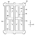
도 5는 본 실시 형태의 제1 구성예에 있어서의 액정 표시 패널의 대향 기판에 있어서의 1화소의 구조를 개략적으로 도시하는 평면도이다.
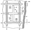
도 6은 본 실시 형태의 제1 구성예에 있어서의 액정 표시 패널의 1화소를 대향 기판측에서 보았을 때의 어레이 기판의 구조를 개략적으로 도시하는 평면도이다.
도 7은 본 실시 형태의 제2 구성예에 있어서의 액정 표시 패널의 대향 기판에 있어서의 1화소의 구조를 개략적으로 도시하는 평면도이다.
도 8은 본 실시 형태의 제2 구성예에 있어서의 액정 표시 패널의 1화소를 대향 기판측에서 보았을 때의 어레이 기판의 구조를 개략적으로 도시하는 평면도이다.
도 9는 본 실시 형태의 제3 구성예에 있어서의 액정 표시 패널의 대향 기판에 있어서의 1화소의 구조를 개략적으로 도시하는 평면도이다.
도 10은 본 실시 형태의 제3 구성예에 있어서의 액정 표시 패널의 1화소를 대향 기판측에서 보았을 때의 어레이 기판의 구조를 개략적으로 도시하는 평면도이다.
도 11은 본 실시 형태의 제4 구성예에 있어서의 액정 표시 패널의 1화소를 대향 기판측에서 보았을 때의 어레이 기판의 구조를 개략적으로 도시하는 평면도이다.
도 12는 제1 내지 제4 구성예에서 설명한 어레이 기판과, 제1 내지 제3 구성예에서 설명한 대향 기판과의 조합을 정리한 도면이다.
도 13은 본 실시 형태의 배리에이션의 하나를 개략적으로 도시하는 평면도이다.
Claims (11)
- 제1 방향을 따라 각각 연장된 게이트 배선 및 보조 용량선과, 제1 방향에 교차하는 제2 방향을 따라 각각 연장된 제1 소스 배선 및 제2 소스 배선과, 상기 제1 소스 배선과 상기 제2 소스 배선과의 사이에 위치하고 제2 방향을 따라 연장된 띠 형상의 주화소 전극과, 상기 주화소 전극에 연결되고 상기 제1 소스 배선 및 상기 제2 소스 배선을 향해 제1 방향을 따라 각각 연장된 띠 형상의 부화소 전극과, 상기 게이트 배선과 대향하고 제1 방향을 따라 연장된 제1 부공통 전극과, 수평 배향성을 나타내는 재료에 의해 형성되고 상기 주화소 전극, 상기 부화소 전극 및 상기 제1 부공통 전극을 덮는 제1 배향막을 구비한 제1 기판과,
상기 주화소 전극을 사이에 둔 양측에서 제2 방향을 따라 각각 연장되고 상기 제1 부공통 전극과 동일 전위의 제2 주공통 전극과, 수평 배향성을 나타내는 재료에 의해 형성되고 상기 제2 주공통 전극을 덮는 제2 배향막을 구비한 제2 기판과,
상기 제1 기판과 상기 제2 기판과의 사이에 보유 지지된 액정 분자를 포함하는 액정층
을 구비한 것을 특징으로 하는 액정 표시 장치. - 제1항에 있어서,
상기 주화소 전극과 상기 제2 주공통 전극과의 사이에 전계가 형성되어 있지 않은 상태에서, 상기 액정 분자의 초기 배향 방향은, 제2 방향에 평행한 것을 특징으로 하는 액정 표시 장치. - 제2항에 있어서,
상기 제1 기판은, 상기 제1 부공통 전극과 연결되고 상기 제1 소스 배선 및 상기 제2 소스 배선과 각각 대향하고 제2 방향을 따라 연장되고 상기 제1 배향막에 의해 덮여진 제1 주공통 전극을 더 구비한 것을 특징으로 하는 액정 표시 장치. - 제1항 내지 제3항 중 어느 한 항에 있어서,
상기 부화소 전극은, 상기 보조 용량선 또는 상기 게이트 배선의 상방에 위치하는 것을 특징으로 하는 액정 표시 장치. - 제4항에 있어서,
상기 부화소 전극은, 상기 주화소 전극의 제2 방향을 따른 중앙부에 결합한 것을 특징으로 하는 액정 표시 장치. - 제5항에 있어서,
상기 부화소 전극은, 상기 주화소 전극과 직교하고 있는 것을 특징으로 하는 액정 표시 장치. - 제6항에 있어서,
상기 주화소 전극은, 상기 제1 소스 배선과 상기 제2 소스 배선과의 중간에 위치하고 있는 것을 특징으로 하는 액정 표시 장치. - 제1항 내지 제3항 중 어느 한 항에 있어서,
상기 제2 주공통 전극은, 상기 제1 소스 배선 및 상기 제2 소스 배선의 상방에 각각 위치하는 것을 특징으로 하는 액정 표시 장치. - 제1항 내지 제3항 중 어느 한 항에 있어서,
상기 제1 배향막이 상기 액정 분자를 초기 배향시키는 제1 배향 처리 방향 및 상기 제2 배향막이 상기 액정 분자를 초기 배향시키는 제2 배향 처리 방향은 서로 평행하며,
상기 액정 분자는, 상기 제1 기판과 상기 제2 기판과의 사이에 있어서 스프레이 배향 또는 호모지니어스 배향되어 있는 것을 특징으로 하는 액정 표시 장치. - 제9항에 있어서,
상기 제1 기판의 외면에 배치되고 제1 편광축을 구비한 제1 편광판과, 제2 기판의 외면에 배치되고 제1 편광축과 크로스 니콜의 위치 관계에 있는 제2 편광축을 구비한 제2 편광판을 더 구비하고, 상기 제1 편광판의 제1 편광축이 상기 액정 분자의 초기 배향 방향과 직교하거나 혹은 평행한 것을 특징으로 하는 액정 표시 장치. - 제1항 내지 제3항 중 어느 한 항에 있어서,
상기 제1 기판은, 용량 결합 구동을 행하기 위한 구동 기구를 구비한 것을 특징으로 하는 액정 표시 장치.
Applications Claiming Priority (3)
| Application Number | Priority Date | Filing Date | Title |
|---|---|---|---|
| JP2011086561 | 2011-04-08 | ||
| JPJP-P-2011-086561 | 2011-04-08 | ||
| PCT/JP2012/053545 WO2012137541A1 (ja) | 2011-04-08 | 2012-02-15 | 液晶表示装置 |
Related Parent Applications (1)
| Application Number | Title | Priority Date | Filing Date |
|---|---|---|---|
| KR1020137026157A Division KR20130131466A (ko) | 2011-04-08 | 2012-02-15 | 액정 표시 장치 |
Publications (1)
| Publication Number | Publication Date |
|---|---|
| KR20140133963A true KR20140133963A (ko) | 2014-11-20 |
Family
ID=46968945
Family Applications (3)
| Application Number | Title | Priority Date | Filing Date |
|---|---|---|---|
| KR1020147030621A Ceased KR20140133963A (ko) | 2011-04-08 | 2012-02-15 | 액정 표시 장치 |
| KR1020137026157A Ceased KR20130131466A (ko) | 2011-04-08 | 2012-02-15 | 액정 표시 장치 |
| KR1020147030620A Ceased KR20140133962A (ko) | 2011-04-08 | 2012-02-15 | 액정 표시 장치 |
Family Applications After (2)
| Application Number | Title | Priority Date | Filing Date |
|---|---|---|---|
| KR1020137026157A Ceased KR20130131466A (ko) | 2011-04-08 | 2012-02-15 | 액정 표시 장치 |
| KR1020147030620A Ceased KR20140133962A (ko) | 2011-04-08 | 2012-02-15 | 액정 표시 장치 |
Country Status (5)
| Country | Link |
|---|---|
| US (1) | US9424786B2 (ko) |
| JP (1) | JP5707488B2 (ko) |
| KR (3) | KR20140133963A (ko) |
| CN (1) | CN103460124B (ko) |
| WO (1) | WO2012137541A1 (ko) |
Families Citing this family (12)
| Publication number | Priority date | Publication date | Assignee | Title |
|---|---|---|---|---|
| JP5953120B2 (ja) | 2012-05-25 | 2016-07-20 | 株式会社ジャパンディスプレイ | 液晶表示装置 |
| JP6093575B2 (ja) | 2013-01-15 | 2017-03-08 | 株式会社ジャパンディスプレイ | 液晶表示装置 |
| JP6093577B2 (ja) * | 2013-01-15 | 2017-03-08 | 株式会社ジャパンディスプレイ | 液晶表示装置 |
| JP2014178490A (ja) | 2013-03-14 | 2014-09-25 | Japan Display Inc | 液晶表示装置 |
| JP2016133771A (ja) | 2015-01-22 | 2016-07-25 | 株式会社ジャパンディスプレイ | 液晶表示装置 |
| CN104597665B (zh) * | 2015-02-13 | 2017-12-26 | 厦门天马微电子有限公司 | 一种液晶显示面板及其制作方法 |
| CN105549290B (zh) * | 2016-02-01 | 2019-07-23 | 京东方科技集团股份有限公司 | 显示面板和显示装置 |
| TWI584034B (zh) * | 2016-09-14 | 2017-05-21 | 友達光電股份有限公司 | 顯示面板 |
| CN106814506B (zh) * | 2017-04-01 | 2018-09-04 | 深圳市华星光电技术有限公司 | 一种液晶显示面板及装置 |
| CN107274851A (zh) * | 2017-08-14 | 2017-10-20 | 京东方科技集团股份有限公司 | 显示面板及其驱动方法和显示装置 |
| JP7083736B2 (ja) * | 2018-10-26 | 2022-06-13 | 株式会社ジャパンディスプレイ | 表示装置 |
| CN117518628A (zh) * | 2023-01-31 | 2024-02-06 | Tcl华星光电技术有限公司 | 像素结构 |
Family Cites Families (34)
| Publication number | Priority date | Publication date | Assignee | Title |
|---|---|---|---|---|
| JPH06222397A (ja) * | 1993-01-25 | 1994-08-12 | Sony Corp | 液晶表示装置 |
| JP2701698B2 (ja) * | 1993-07-20 | 1998-01-21 | 株式会社日立製作所 | 液晶表示装置 |
| TW454101B (en) | 1995-10-04 | 2001-09-11 | Hitachi Ltd | In-plane field type liquid crystal display device comprising liquid crystal molecules with more than two different kinds of reorientation directions and its manufacturing method |
| JPH09160061A (ja) | 1995-12-08 | 1997-06-20 | Toshiba Corp | 液晶表示素子 |
| JPH09160042A (ja) | 1995-12-08 | 1997-06-20 | Toshiba Corp | 液晶表示素子 |
| JPH09160041A (ja) | 1995-12-08 | 1997-06-20 | Toshiba Corp | 液晶表示素子 |
| JPH1026765A (ja) | 1996-07-10 | 1998-01-27 | Toshiba Corp | 液晶表示素子、投影型液晶表示装置及び基板 |
| JP3644653B2 (ja) | 1996-08-07 | 2005-05-11 | 三菱電機株式会社 | 液晶表示装置 |
| JPH1090708A (ja) | 1996-09-17 | 1998-04-10 | Toshiba Corp | 液晶表示素子 |
| JPH10186366A (ja) * | 1996-12-26 | 1998-07-14 | Fujitsu Ltd | 液晶表示装置 |
| TW451099B (en) | 1998-01-23 | 2001-08-21 | Hitachi Ltd | Liquid crystal display device |
| JP4364332B2 (ja) | 1998-06-23 | 2009-11-18 | シャープ株式会社 | 液晶表示装置 |
| JP3132483B2 (ja) * | 1998-09-17 | 2001-02-05 | 日本電気株式会社 | 横電界方式の液晶表示装置 |
| KR100303351B1 (ko) | 1998-12-17 | 2002-06-20 | 박종섭 | 수직 배향 모드 액정 표시 장치 |
| JP2001282205A (ja) * | 2000-03-31 | 2001-10-12 | Matsushita Electric Ind Co Ltd | アクティブマトリクス型液晶表示装置およびその駆動方法 |
| JP2002040457A (ja) * | 2000-07-31 | 2002-02-06 | Sanyo Electric Co Ltd | 液晶表示装置 |
| TWI298110B (en) * | 2001-07-31 | 2008-06-21 | Hitachi Ltd | Liquid crystal display device |
| JP4107978B2 (ja) | 2003-02-21 | 2008-06-25 | スタンレー電気株式会社 | 液晶表示素子 |
| KR100698047B1 (ko) | 2003-04-19 | 2007-03-23 | 엘지.필립스 엘시디 주식회사 | 횡전계형 액정 표시 장치 및 그 제조 방법 |
| JP2005003802A (ja) | 2003-06-10 | 2005-01-06 | Toshiba Matsushita Display Technology Co Ltd | 液晶表示装置 |
| KR100959367B1 (ko) * | 2003-10-13 | 2010-05-25 | 엘지디스플레이 주식회사 | 횡전계형 액정표시장치 |
| JP4088619B2 (ja) | 2004-01-28 | 2008-05-21 | シャープ株式会社 | アクティブマトリクス基板及び表示装置 |
| KR100617040B1 (ko) | 2004-03-16 | 2006-08-30 | 엘지.필립스 엘시디 주식회사 | 횡전계방식 액정표시소자 및 그 제조방법 |
| JP2005292515A (ja) | 2004-03-31 | 2005-10-20 | Sharp Corp | 液晶表示装置およびその駆動方法ならびに電子機器 |
| KR100672216B1 (ko) | 2004-11-03 | 2007-01-22 | 엘지.필립스 엘시디 주식회사 | 액정표시장치 |
| JP4202354B2 (ja) * | 2005-10-31 | 2008-12-24 | エルジー ディスプレイ カンパニー リミテッド | 液晶表示装置 |
| KR101247113B1 (ko) | 2005-11-22 | 2013-04-01 | 삼성디스플레이 주식회사 | 표시장치 |
| TW200813535A (en) | 2006-09-12 | 2008-03-16 | Wintek Corp | Liquid crystal panel and liquid crystal display |
| KR101413275B1 (ko) | 2007-01-29 | 2014-06-30 | 삼성디스플레이 주식회사 | 액정 표시 패널 및 이의 제조 방법 |
| KR20080071231A (ko) * | 2007-01-30 | 2008-08-04 | 삼성전자주식회사 | 액정 표시 장치 |
| KR101427708B1 (ko) | 2007-02-01 | 2014-08-11 | 삼성디스플레이 주식회사 | 액정 표시 패널 |
| JP5093724B2 (ja) * | 2007-10-29 | 2012-12-12 | Nltテクノロジー株式会社 | 液晶表示装置 |
| JP4693131B2 (ja) * | 2008-02-14 | 2011-06-01 | 東芝モバイルディスプレイ株式会社 | 液晶表示装置 |
| JP2009244287A (ja) * | 2008-03-28 | 2009-10-22 | Toshiba Mobile Display Co Ltd | 液晶表示装置および液晶表示装置の駆動方法 |
-
2012
- 2012-02-15 WO PCT/JP2012/053545 patent/WO2012137541A1/ja not_active Ceased
- 2012-02-15 CN CN201280016433.5A patent/CN103460124B/zh not_active Expired - Fee Related
- 2012-02-15 KR KR1020147030621A patent/KR20140133963A/ko not_active Ceased
- 2012-02-15 KR KR1020137026157A patent/KR20130131466A/ko not_active Ceased
- 2012-02-15 JP JP2013508784A patent/JP5707488B2/ja not_active Expired - Fee Related
- 2012-02-15 KR KR1020147030620A patent/KR20140133962A/ko not_active Ceased
-
2013
- 2013-10-08 US US14/048,552 patent/US9424786B2/en active Active
Also Published As
| Publication number | Publication date |
|---|---|
| US9424786B2 (en) | 2016-08-23 |
| CN103460124A (zh) | 2013-12-18 |
| WO2012137541A1 (ja) | 2012-10-11 |
| CN103460124B (zh) | 2016-08-10 |
| KR20140133962A (ko) | 2014-11-20 |
| JPWO2012137541A1 (ja) | 2014-07-28 |
| US20140055430A1 (en) | 2014-02-27 |
| KR20130131466A (ko) | 2013-12-03 |
| JP5707488B2 (ja) | 2015-04-30 |
Similar Documents
| Publication | Publication Date | Title |
|---|---|---|
| KR101635668B1 (ko) | 액정 표시 장치 | |
| JP5707488B2 (ja) | 液晶表示装置 | |
| JP5386555B2 (ja) | 液晶表示装置 | |
| JP5560247B2 (ja) | 液晶表示装置 | |
| JP5552457B2 (ja) | 液晶表示装置 | |
| JP5759813B2 (ja) | 液晶表示装置 | |
| CN102778790B (zh) | 液晶显示设备 | |
| JP6063710B2 (ja) | 液晶表示装置 | |
| JP2014112195A (ja) | 液晶表示装置 | |
| JP5674587B2 (ja) | 液晶表示装置 | |
| JP5377567B2 (ja) | 液晶表示装置 | |
| JP6010330B2 (ja) | 液晶表示装置 | |
| JP5785831B2 (ja) | 液晶表示装置 | |
| JP5845042B2 (ja) | 液晶表示装置 | |
| JP5851175B2 (ja) | 液晶表示装置 | |
| JP5816496B2 (ja) | 液晶表示装置 | |
| JP5785834B2 (ja) | 液晶表示装置 | |
| JP5824301B2 (ja) | 液晶表示装置 | |
| JP2015072374A (ja) | 液晶表示装置 |
Legal Events
| Date | Code | Title | Description |
|---|---|---|---|
| A107 | Divisional application of patent | ||
| A201 | Request for examination | ||
| PA0104 | Divisional application for international application |
Comment text: Divisional Application for International Patent Patent event code: PA01041R01D Patent event date: 20141030 Application number text: 1020137026157 Filing date: 20131002 |
|
| PA0201 | Request for examination | ||
| PG1501 | Laying open of application | ||
| E902 | Notification of reason for refusal | ||
| PE0902 | Notice of grounds for rejection |
Comment text: Notification of reason for refusal Patent event date: 20141128 Patent event code: PE09021S01D |
|
| E601 | Decision to refuse application | ||
| PE0601 | Decision on rejection of patent |
Patent event date: 20150520 Comment text: Decision to Refuse Application Patent event code: PE06012S01D Patent event date: 20141128 Comment text: Notification of reason for refusal Patent event code: PE06011S01I |