KR20140140742A - 가요성 표시 장치 및 가요성 표시 장치의 제조 방법 - Google Patents
가요성 표시 장치 및 가요성 표시 장치의 제조 방법 Download PDFInfo
- Publication number
- KR20140140742A KR20140140742A KR20130061492A KR20130061492A KR20140140742A KR 20140140742 A KR20140140742 A KR 20140140742A KR 20130061492 A KR20130061492 A KR 20130061492A KR 20130061492 A KR20130061492 A KR 20130061492A KR 20140140742 A KR20140140742 A KR 20140140742A
- Authority
- KR
- South Korea
- Prior art keywords
- display device
- layer
- display area
- substrate
- light emitting
- Prior art date
- Legal status (The legal status is an assumption and is not a legal conclusion. Google has not performed a legal analysis and makes no representation as to the accuracy of the status listed.)
- Granted
Links
- 238000004519 manufacturing process Methods 0.000 title claims description 10
- 239000000758 substrate Substances 0.000 claims abstract description 90
- 239000002105 nanoparticle Substances 0.000 claims abstract description 38
- 229910052710 silicon Inorganic materials 0.000 claims abstract description 20
- 239000010703 silicon Substances 0.000 claims abstract description 20
- 230000002093 peripheral effect Effects 0.000 claims abstract description 10
- 239000010410 layer Substances 0.000 claims description 139
- 239000012044 organic layer Substances 0.000 claims description 76
- 238000000034 method Methods 0.000 claims description 57
- OKTJSMMVPCPJKN-UHFFFAOYSA-N Carbon Chemical compound [C] OKTJSMMVPCPJKN-UHFFFAOYSA-N 0.000 claims description 36
- 239000000463 material Substances 0.000 claims description 36
- 238000002347 injection Methods 0.000 claims description 32
- 239000007924 injection Substances 0.000 claims description 32
- 239000002041 carbon nanotube Substances 0.000 claims description 27
- XUIMIQQOPSSXEZ-UHFFFAOYSA-N Silicon Chemical compound [Si] XUIMIQQOPSSXEZ-UHFFFAOYSA-N 0.000 claims description 19
- XMWRBQBLMFGWIX-UHFFFAOYSA-N C60 fullerene Chemical class C12=C3C(C4=C56)=C7C8=C5C5=C9C%10=C6C6=C4C1=C1C4=C6C6=C%10C%10=C9C9=C%11C5=C8C5=C8C7=C3C3=C7C2=C1C1=C2C4=C6C4=C%10C6=C9C9=C%11C5=C5C8=C3C3=C7C1=C1C2=C4C6=C2C9=C5C3=C12 XMWRBQBLMFGWIX-UHFFFAOYSA-N 0.000 claims description 15
- 229910003472 fullerene Inorganic materials 0.000 claims description 15
- 239000002096 quantum dot Substances 0.000 claims description 15
- 229910021389 graphene Inorganic materials 0.000 claims description 11
- 230000005525 hole transport Effects 0.000 claims description 10
- 229910021417 amorphous silicon Inorganic materials 0.000 claims description 7
- 238000000576 coating method Methods 0.000 claims description 7
- 229910021421 monocrystalline silicon Inorganic materials 0.000 claims description 7
- 229910021420 polycrystalline silicon Inorganic materials 0.000 claims description 7
- 238000007639 printing Methods 0.000 claims description 6
- 238000007641 inkjet printing Methods 0.000 claims description 3
- 238000007650 screen-printing Methods 0.000 claims description 3
- 238000004528 spin coating Methods 0.000 claims description 3
- 238000005507 spraying Methods 0.000 claims description 3
- 238000005452 bending Methods 0.000 abstract description 4
- 238000005096 rolling process Methods 0.000 abstract description 4
- 239000010408 film Substances 0.000 description 32
- 229910021393 carbon nanotube Inorganic materials 0.000 description 24
- 239000011229 interlayer Substances 0.000 description 16
- 239000000872 buffer Substances 0.000 description 9
- 229910052783 alkali metal Inorganic materials 0.000 description 8
- 150000001340 alkali metals Chemical class 0.000 description 8
- 229910052784 alkaline earth metal Inorganic materials 0.000 description 8
- 150000001342 alkaline earth metals Chemical class 0.000 description 8
- 238000005229 chemical vapour deposition Methods 0.000 description 8
- -1 grephene Chemical compound 0.000 description 8
- 229910052782 aluminium Inorganic materials 0.000 description 7
- XLOMVQKBTHCTTD-UHFFFAOYSA-N Zinc monoxide Chemical compound [Zn]=O XLOMVQKBTHCTTD-UHFFFAOYSA-N 0.000 description 6
- 239000004020 conductor Substances 0.000 description 6
- 229920000767 polyaniline Polymers 0.000 description 6
- VYPSYNLAJGMNEJ-UHFFFAOYSA-N Silicium dioxide Chemical compound O=[Si]=O VYPSYNLAJGMNEJ-UHFFFAOYSA-N 0.000 description 5
- RTAQQCXQSZGOHL-UHFFFAOYSA-N Titanium Chemical compound [Ti] RTAQQCXQSZGOHL-UHFFFAOYSA-N 0.000 description 5
- XAGFODPZIPBFFR-UHFFFAOYSA-N aluminium Chemical compound [Al] XAGFODPZIPBFFR-UHFFFAOYSA-N 0.000 description 5
- 238000012986 modification Methods 0.000 description 5
- 230000004048 modification Effects 0.000 description 5
- 229910052757 nitrogen Inorganic materials 0.000 description 5
- 239000011347 resin Substances 0.000 description 5
- 229920005989 resin Polymers 0.000 description 5
- 229910052814 silicon oxide Inorganic materials 0.000 description 5
- 229910052719 titanium Inorganic materials 0.000 description 5
- 239000010936 titanium Substances 0.000 description 5
- VIJYEGDOKCKUOL-UHFFFAOYSA-N 9-phenylcarbazole Chemical compound C1=CC=CC=C1N1C2=CC=CC=C2C2=CC=CC=C21 VIJYEGDOKCKUOL-UHFFFAOYSA-N 0.000 description 4
- 239000004925 Acrylic resin Substances 0.000 description 4
- KRHYYFGTRYWZRS-UHFFFAOYSA-M Fluoride anion Chemical compound [F-] KRHYYFGTRYWZRS-UHFFFAOYSA-M 0.000 description 4
- 238000000231 atomic layer deposition Methods 0.000 description 4
- 229910010272 inorganic material Inorganic materials 0.000 description 4
- 239000011147 inorganic material Substances 0.000 description 4
- 239000011368 organic material Substances 0.000 description 4
- IEQIEDJGQAUEQZ-UHFFFAOYSA-N phthalocyanine Chemical compound N1C(N=C2C3=CC=CC=C3C(N=C3C4=CC=CC=C4C(=N4)N3)=N2)=C(C=CC=C2)C2=C1N=C1C2=CC=CC=C2C4=N1 IEQIEDJGQAUEQZ-UHFFFAOYSA-N 0.000 description 4
- 238000000623 plasma-assisted chemical vapour deposition Methods 0.000 description 4
- BASFCYQUMIYNBI-UHFFFAOYSA-N platinum Chemical compound [Pt] BASFCYQUMIYNBI-UHFFFAOYSA-N 0.000 description 4
- 229920003227 poly(N-vinyl carbazole) Polymers 0.000 description 4
- 238000004544 sputter deposition Methods 0.000 description 4
- 238000001771 vacuum deposition Methods 0.000 description 4
- 125000001637 1-naphthyl group Chemical group [H]C1=C([H])C([H])=C2C(*)=C([H])C([H])=C([H])C2=C1[H] 0.000 description 3
- VYZAMTAEIAYCRO-UHFFFAOYSA-N Chromium Chemical compound [Cr] VYZAMTAEIAYCRO-UHFFFAOYSA-N 0.000 description 3
- ZOKXTWBITQBERF-UHFFFAOYSA-N Molybdenum Chemical compound [Mo] ZOKXTWBITQBERF-UHFFFAOYSA-N 0.000 description 3
- 229910045601 alloy Inorganic materials 0.000 description 3
- 239000000956 alloy Substances 0.000 description 3
- 229910052804 chromium Inorganic materials 0.000 description 3
- 239000011651 chromium Substances 0.000 description 3
- 150000001875 compounds Chemical class 0.000 description 3
- 230000014509 gene expression Effects 0.000 description 3
- AMGQUBHHOARCQH-UHFFFAOYSA-N indium;oxotin Chemical compound [In].[Sn]=O AMGQUBHHOARCQH-UHFFFAOYSA-N 0.000 description 3
- 229910052750 molybdenum Inorganic materials 0.000 description 3
- 239000011733 molybdenum Substances 0.000 description 3
- 238000000059 patterning Methods 0.000 description 3
- 239000004065 semiconductor Substances 0.000 description 3
- 150000003377 silicon compounds Chemical class 0.000 description 3
- 239000010409 thin film Substances 0.000 description 3
- XOLBLPGZBRYERU-UHFFFAOYSA-N tin dioxide Chemical compound O=[Sn]=O XOLBLPGZBRYERU-UHFFFAOYSA-N 0.000 description 3
- 229910001887 tin oxide Inorganic materials 0.000 description 3
- TVIVIEFSHFOWTE-UHFFFAOYSA-K tri(quinolin-8-yloxy)alumane Chemical compound [Al+3].C1=CN=C2C([O-])=CC=CC2=C1.C1=CN=C2C([O-])=CC=CC2=C1.C1=CN=C2C([O-])=CC=CC2=C1 TVIVIEFSHFOWTE-UHFFFAOYSA-K 0.000 description 3
- WFKWXMTUELFFGS-UHFFFAOYSA-N tungsten Chemical compound [W] WFKWXMTUELFFGS-UHFFFAOYSA-N 0.000 description 3
- 229910052721 tungsten Inorganic materials 0.000 description 3
- 239000010937 tungsten Substances 0.000 description 3
- YVTHLONGBIQYBO-UHFFFAOYSA-N zinc indium(3+) oxygen(2-) Chemical compound [O--].[Zn++].[In+3] YVTHLONGBIQYBO-UHFFFAOYSA-N 0.000 description 3
- 239000011787 zinc oxide Substances 0.000 description 3
- OGGKVJMNFFSDEV-UHFFFAOYSA-N 3-methyl-n-[4-[4-(n-(3-methylphenyl)anilino)phenyl]phenyl]-n-phenylaniline Chemical group CC1=CC=CC(N(C=2C=CC=CC=2)C=2C=CC(=CC=2)C=2C=CC(=CC=2)N(C=2C=CC=CC=2)C=2C=C(C)C=CC=2)=C1 OGGKVJMNFFSDEV-UHFFFAOYSA-N 0.000 description 2
- 229920000178 Acrylic resin Polymers 0.000 description 2
- IJGRMHOSHXDMSA-UHFFFAOYSA-N Atomic nitrogen Chemical compound N#N IJGRMHOSHXDMSA-UHFFFAOYSA-N 0.000 description 2
- RYGMFSIKBFXOCR-UHFFFAOYSA-N Copper Chemical compound [Cu] RYGMFSIKBFXOCR-UHFFFAOYSA-N 0.000 description 2
- PXHVJJICTQNCMI-UHFFFAOYSA-N Nickel Chemical compound [Ni] PXHVJJICTQNCMI-UHFFFAOYSA-N 0.000 description 2
- KDLHZDBZIXYQEI-UHFFFAOYSA-N Palladium Chemical compound [Pd] KDLHZDBZIXYQEI-UHFFFAOYSA-N 0.000 description 2
- 229920001609 Poly(3,4-ethylenedioxythiophene) Polymers 0.000 description 2
- 239000004721 Polyphenylene oxide Substances 0.000 description 2
- 229910052581 Si3N4 Inorganic materials 0.000 description 2
- QCWXUUIWCKQGHC-UHFFFAOYSA-N Zirconium Chemical compound [Zr] QCWXUUIWCKQGHC-UHFFFAOYSA-N 0.000 description 2
- 238000007792 addition Methods 0.000 description 2
- UFVXQDWNSAGPHN-UHFFFAOYSA-K bis[(2-methylquinolin-8-yl)oxy]-(4-phenylphenoxy)alumane Chemical compound [Al+3].C1=CC=C([O-])C2=NC(C)=CC=C21.C1=CC=C([O-])C2=NC(C)=CC=C21.C1=CC([O-])=CC=C1C1=CC=CC=C1 UFVXQDWNSAGPHN-UHFFFAOYSA-K 0.000 description 2
- 229910052802 copper Inorganic materials 0.000 description 2
- 239000010949 copper Substances 0.000 description 2
- 229910000449 hafnium oxide Inorganic materials 0.000 description 2
- WIHZLLGSGQNAGK-UHFFFAOYSA-N hafnium(4+);oxygen(2-) Chemical compound [O-2].[O-2].[Hf+4] WIHZLLGSGQNAGK-UHFFFAOYSA-N 0.000 description 2
- 239000012535 impurity Substances 0.000 description 2
- 229910052751 metal Inorganic materials 0.000 description 2
- 239000002184 metal Substances 0.000 description 2
- 229910044991 metal oxide Inorganic materials 0.000 description 2
- 150000004706 metal oxides Chemical class 0.000 description 2
- 230000003647 oxidation Effects 0.000 description 2
- 238000007254 oxidation reaction Methods 0.000 description 2
- TWNQGVIAIRXVLR-UHFFFAOYSA-N oxo(oxoalumanyloxy)alumane Chemical compound O=[Al]O[Al]=O TWNQGVIAIRXVLR-UHFFFAOYSA-N 0.000 description 2
- BPUBBGLMJRNUCC-UHFFFAOYSA-N oxygen(2-);tantalum(5+) Chemical compound [O-2].[O-2].[O-2].[O-2].[O-2].[Ta+5].[Ta+5] BPUBBGLMJRNUCC-UHFFFAOYSA-N 0.000 description 2
- RVTZCBVAJQQJTK-UHFFFAOYSA-N oxygen(2-);zirconium(4+) Chemical compound [O-2].[O-2].[Zr+4] RVTZCBVAJQQJTK-UHFFFAOYSA-N 0.000 description 2
- 229910052697 platinum Inorganic materials 0.000 description 2
- 229920005668 polycarbonate resin Polymers 0.000 description 2
- 239000004431 polycarbonate resin Substances 0.000 description 2
- 229920000570 polyether Polymers 0.000 description 2
- 229920000139 polyethylene terephthalate Polymers 0.000 description 2
- 239000005020 polyethylene terephthalate Substances 0.000 description 2
- 229920001721 polyimide Polymers 0.000 description 2
- 239000009719 polyimide resin Substances 0.000 description 2
- HQVNEWCFYHHQES-UHFFFAOYSA-N silicon nitride Chemical compound N12[Si]34N5[Si]62N3[Si]51N64 HQVNEWCFYHHQES-UHFFFAOYSA-N 0.000 description 2
- 229910001936 tantalum oxide Inorganic materials 0.000 description 2
- 229910052726 zirconium Inorganic materials 0.000 description 2
- 229910001928 zirconium oxide Inorganic materials 0.000 description 2
- LSNNMFCWUKXFEE-UHFFFAOYSA-M Bisulfite Chemical compound OS([O-])=O LSNNMFCWUKXFEE-UHFFFAOYSA-M 0.000 description 1
- GYHNNYVSQQEPJS-UHFFFAOYSA-N Gallium Chemical compound [Ga] GYHNNYVSQQEPJS-UHFFFAOYSA-N 0.000 description 1
- DGAQECJNVWCQMB-PUAWFVPOSA-M Ilexoside XXIX Chemical compound C[C@@H]1CC[C@@]2(CC[C@@]3(C(=CC[C@H]4[C@]3(CC[C@@H]5[C@@]4(CC[C@@H](C5(C)C)OS(=O)(=O)[O-])C)C)[C@@H]2[C@]1(C)O)C)C(=O)O[C@H]6[C@@H]([C@H]([C@@H]([C@H](O6)CO)O)O)O.[Na+] DGAQECJNVWCQMB-PUAWFVPOSA-M 0.000 description 1
- WHXSMMKQMYFTQS-UHFFFAOYSA-N Lithium Chemical compound [Li] WHXSMMKQMYFTQS-UHFFFAOYSA-N 0.000 description 1
- 229910052779 Neodymium Inorganic materials 0.000 description 1
- OAICVXFJPJFONN-UHFFFAOYSA-N Phosphorus Chemical compound [P] OAICVXFJPJFONN-UHFFFAOYSA-N 0.000 description 1
- KJTLSVCANCCWHF-UHFFFAOYSA-N Ruthenium Chemical compound [Ru] KJTLSVCANCCWHF-UHFFFAOYSA-N 0.000 description 1
- BQCADISMDOOEFD-UHFFFAOYSA-N Silver Chemical compound [Ag] BQCADISMDOOEFD-UHFFFAOYSA-N 0.000 description 1
- ATJFFYVFTNAWJD-UHFFFAOYSA-N Tin Chemical compound [Sn] ATJFFYVFTNAWJD-UHFFFAOYSA-N 0.000 description 1
- 239000007983 Tris buffer Substances 0.000 description 1
- HCHKCACWOHOZIP-UHFFFAOYSA-N Zinc Chemical compound [Zn] HCHKCACWOHOZIP-UHFFFAOYSA-N 0.000 description 1
- 125000004429 atom Chemical group 0.000 description 1
- 230000015572 biosynthetic process Effects 0.000 description 1
- 229910052799 carbon Inorganic materials 0.000 description 1
- 125000004432 carbon atom Chemical group C* 0.000 description 1
- 238000009792 diffusion process Methods 0.000 description 1
- 230000000694 effects Effects 0.000 description 1
- 229910052733 gallium Inorganic materials 0.000 description 1
- 229910052732 germanium Inorganic materials 0.000 description 1
- GNPVGFCGXDBREM-UHFFFAOYSA-N germanium atom Chemical compound [Ge] GNPVGFCGXDBREM-UHFFFAOYSA-N 0.000 description 1
- 239000011521 glass Substances 0.000 description 1
- 229910052735 hafnium Inorganic materials 0.000 description 1
- VBJZVLUMGGDVMO-UHFFFAOYSA-N hafnium atom Chemical compound [Hf] VBJZVLUMGGDVMO-UHFFFAOYSA-N 0.000 description 1
- 239000003779 heat-resistant material Substances 0.000 description 1
- 229910052738 indium Inorganic materials 0.000 description 1
- APFVFJFRJDLVQX-UHFFFAOYSA-N indium atom Chemical compound [In] APFVFJFRJDLVQX-UHFFFAOYSA-N 0.000 description 1
- 239000012212 insulator Substances 0.000 description 1
- 239000007788 liquid Substances 0.000 description 1
- 229910052744 lithium Inorganic materials 0.000 description 1
- WPBNNNQJVZRUHP-UHFFFAOYSA-L manganese(2+);methyl n-[[2-(methoxycarbonylcarbamothioylamino)phenyl]carbamothioyl]carbamate;n-[2-(sulfidocarbothioylamino)ethyl]carbamodithioate Chemical compound [Mn+2].[S-]C(=S)NCCNC([S-])=S.COC(=O)NC(=S)NC1=CC=CC=C1NC(=S)NC(=O)OC WPBNNNQJVZRUHP-UHFFFAOYSA-L 0.000 description 1
- 239000000203 mixture Substances 0.000 description 1
- IBHBKWKFFTZAHE-UHFFFAOYSA-N n-[4-[4-(n-naphthalen-1-ylanilino)phenyl]phenyl]-n-phenylnaphthalen-1-amine Chemical group C1=CC=CC=C1N(C=1C2=CC=CC=C2C=CC=1)C1=CC=C(C=2C=CC(=CC=2)N(C=2C=CC=CC=2)C=2C3=CC=CC=C3C=CC=2)C=C1 IBHBKWKFFTZAHE-UHFFFAOYSA-N 0.000 description 1
- QEFYFXOXNSNQGX-UHFFFAOYSA-N neodymium atom Chemical compound [Nd] QEFYFXOXNSNQGX-UHFFFAOYSA-N 0.000 description 1
- 229910052759 nickel Inorganic materials 0.000 description 1
- 239000003960 organic solvent Substances 0.000 description 1
- KYKLWYKWCAYAJY-UHFFFAOYSA-N oxotin;zinc Chemical compound [Zn].[Sn]=O KYKLWYKWCAYAJY-UHFFFAOYSA-N 0.000 description 1
- 229910052763 palladium Inorganic materials 0.000 description 1
- 229910052698 phosphorus Inorganic materials 0.000 description 1
- 239000011574 phosphorus Substances 0.000 description 1
- 239000004033 plastic Substances 0.000 description 1
- 229920003023 plastic Polymers 0.000 description 1
- 238000004549 pulsed laser deposition Methods 0.000 description 1
- 229910052707 ruthenium Inorganic materials 0.000 description 1
- 229910052709 silver Inorganic materials 0.000 description 1
- 239000004332 silver Substances 0.000 description 1
- 239000002356 single layer Substances 0.000 description 1
- 229910052708 sodium Inorganic materials 0.000 description 1
- 239000011734 sodium Substances 0.000 description 1
- 238000003980 solgel method Methods 0.000 description 1
- 239000007921 spray Substances 0.000 description 1
- 238000006467 substitution reaction Methods 0.000 description 1
- 229910052715 tantalum Inorganic materials 0.000 description 1
- GUVRBAGPIYLISA-UHFFFAOYSA-N tantalum atom Chemical compound [Ta] GUVRBAGPIYLISA-UHFFFAOYSA-N 0.000 description 1
- 229910052718 tin Inorganic materials 0.000 description 1
- 229910052720 vanadium Inorganic materials 0.000 description 1
- GPPXJZIENCGNKB-UHFFFAOYSA-N vanadium Chemical compound [V]#[V] GPPXJZIENCGNKB-UHFFFAOYSA-N 0.000 description 1
- 229910052725 zinc Inorganic materials 0.000 description 1
- 239000011701 zinc Substances 0.000 description 1
Images






Classifications
-
- H—ELECTRICITY
- H10—SEMICONDUCTOR DEVICES; ELECTRIC SOLID-STATE DEVICES NOT OTHERWISE PROVIDED FOR
- H10K—ORGANIC ELECTRIC SOLID-STATE DEVICES
- H10K77/00—Constructional details of devices covered by this subclass and not covered by groups H10K10/80, H10K30/80, H10K50/80 or H10K59/80
- H10K77/10—Substrates, e.g. flexible substrates
- H10K77/111—Flexible substrates
-
- G—PHYSICS
- G09—EDUCATION; CRYPTOGRAPHY; DISPLAY; ADVERTISING; SEALS
- G09F—DISPLAYING; ADVERTISING; SIGNS; LABELS OR NAME-PLATES; SEALS
- G09F9/00—Indicating arrangements for variable information in which the information is built-up on a support by selection or combination of individual elements
-
- H—ELECTRICITY
- H10—SEMICONDUCTOR DEVICES; ELECTRIC SOLID-STATE DEVICES NOT OTHERWISE PROVIDED FOR
- H10K—ORGANIC ELECTRIC SOLID-STATE DEVICES
- H10K50/00—Organic light-emitting devices
- H10K50/10—OLEDs or polymer light-emitting diodes [PLED]
- H10K50/11—OLEDs or polymer light-emitting diodes [PLED] characterised by the electroluminescent [EL] layers
- H10K50/115—OLEDs or polymer light-emitting diodes [PLED] characterised by the electroluminescent [EL] layers comprising active inorganic nanostructures, e.g. luminescent quantum dots
-
- H—ELECTRICITY
- H10—SEMICONDUCTOR DEVICES; ELECTRIC SOLID-STATE DEVICES NOT OTHERWISE PROVIDED FOR
- H10K—ORGANIC ELECTRIC SOLID-STATE DEVICES
- H10K50/00—Organic light-emitting devices
- H10K50/10—OLEDs or polymer light-emitting diodes [PLED]
- H10K50/14—Carrier transporting layers
- H10K50/15—Hole transporting layers
-
- H—ELECTRICITY
- H10—SEMICONDUCTOR DEVICES; ELECTRIC SOLID-STATE DEVICES NOT OTHERWISE PROVIDED FOR
- H10K—ORGANIC ELECTRIC SOLID-STATE DEVICES
- H10K50/00—Organic light-emitting devices
- H10K50/10—OLEDs or polymer light-emitting diodes [PLED]
- H10K50/14—Carrier transporting layers
- H10K50/16—Electron transporting layers
-
- H—ELECTRICITY
- H10—SEMICONDUCTOR DEVICES; ELECTRIC SOLID-STATE DEVICES NOT OTHERWISE PROVIDED FOR
- H10K—ORGANIC ELECTRIC SOLID-STATE DEVICES
- H10K50/00—Organic light-emitting devices
- H10K50/10—OLEDs or polymer light-emitting diodes [PLED]
- H10K50/17—Carrier injection layers
-
- H—ELECTRICITY
- H10—SEMICONDUCTOR DEVICES; ELECTRIC SOLID-STATE DEVICES NOT OTHERWISE PROVIDED FOR
- H10K—ORGANIC ELECTRIC SOLID-STATE DEVICES
- H10K50/00—Organic light-emitting devices
- H10K50/10—OLEDs or polymer light-emitting diodes [PLED]
- H10K50/17—Carrier injection layers
- H10K50/171—Electron injection layers
-
- H—ELECTRICITY
- H10—SEMICONDUCTOR DEVICES; ELECTRIC SOLID-STATE DEVICES NOT OTHERWISE PROVIDED FOR
- H10K—ORGANIC ELECTRIC SOLID-STATE DEVICES
- H10K50/00—Organic light-emitting devices
- H10K50/80—Constructional details
- H10K50/805—Electrodes
-
- H—ELECTRICITY
- H10—SEMICONDUCTOR DEVICES; ELECTRIC SOLID-STATE DEVICES NOT OTHERWISE PROVIDED FOR
- H10K—ORGANIC ELECTRIC SOLID-STATE DEVICES
- H10K50/00—Organic light-emitting devices
- H10K50/80—Constructional details
- H10K50/84—Passivation; Containers; Encapsulations
- H10K50/841—Self-supporting sealing arrangements
-
- H—ELECTRICITY
- H10—SEMICONDUCTOR DEVICES; ELECTRIC SOLID-STATE DEVICES NOT OTHERWISE PROVIDED FOR
- H10K—ORGANIC ELECTRIC SOLID-STATE DEVICES
- H10K59/00—Integrated devices, or assemblies of multiple devices, comprising at least one organic light-emitting element covered by group H10K50/00
- H10K59/10—OLED displays
- H10K59/12—Active-matrix OLED [AMOLED] displays
- H10K59/121—Active-matrix OLED [AMOLED] displays characterised by the geometry or disposition of pixel elements
- H10K59/1213—Active-matrix OLED [AMOLED] displays characterised by the geometry or disposition of pixel elements the pixel elements being TFTs
-
- H—ELECTRICITY
- H10—SEMICONDUCTOR DEVICES; ELECTRIC SOLID-STATE DEVICES NOT OTHERWISE PROVIDED FOR
- H10K—ORGANIC ELECTRIC SOLID-STATE DEVICES
- H10K71/00—Manufacture or treatment specially adapted for the organic devices covered by this subclass
- H10K71/10—Deposition of organic active material
- H10K71/12—Deposition of organic active material using liquid deposition, e.g. spin coating
- H10K71/13—Deposition of organic active material using liquid deposition, e.g. spin coating using printing techniques, e.g. ink-jet printing or screen printing
-
- H—ELECTRICITY
- H10—SEMICONDUCTOR DEVICES; ELECTRIC SOLID-STATE DEVICES NOT OTHERWISE PROVIDED FOR
- H10K—ORGANIC ELECTRIC SOLID-STATE DEVICES
- H10K71/00—Manufacture or treatment specially adapted for the organic devices covered by this subclass
- H10K71/10—Deposition of organic active material
- H10K71/12—Deposition of organic active material using liquid deposition, e.g. spin coating
- H10K71/13—Deposition of organic active material using liquid deposition, e.g. spin coating using printing techniques, e.g. ink-jet printing or screen printing
- H10K71/135—Deposition of organic active material using liquid deposition, e.g. spin coating using printing techniques, e.g. ink-jet printing or screen printing using ink-jet printing
-
- H—ELECTRICITY
- H10—SEMICONDUCTOR DEVICES; ELECTRIC SOLID-STATE DEVICES NOT OTHERWISE PROVIDED FOR
- H10K—ORGANIC ELECTRIC SOLID-STATE DEVICES
- H10K71/00—Manufacture or treatment specially adapted for the organic devices covered by this subclass
- H10K71/10—Deposition of organic active material
- H10K71/16—Deposition of organic active material using physical vapour deposition [PVD], e.g. vacuum deposition or sputtering
-
- H—ELECTRICITY
- H10—SEMICONDUCTOR DEVICES; ELECTRIC SOLID-STATE DEVICES NOT OTHERWISE PROVIDED FOR
- H10K—ORGANIC ELECTRIC SOLID-STATE DEVICES
- H10K2102/00—Constructional details relating to the organic devices covered by this subclass
- H10K2102/301—Details of OLEDs
- H10K2102/311—Flexible OLED
-
- H—ELECTRICITY
- H10—SEMICONDUCTOR DEVICES; ELECTRIC SOLID-STATE DEVICES NOT OTHERWISE PROVIDED FOR
- H10K—ORGANIC ELECTRIC SOLID-STATE DEVICES
- H10K2102/00—Constructional details relating to the organic devices covered by this subclass
- H10K2102/301—Details of OLEDs
- H10K2102/331—Nanoparticles used in non-emissive layers, e.g. in packaging layer
-
- H—ELECTRICITY
- H10—SEMICONDUCTOR DEVICES; ELECTRIC SOLID-STATE DEVICES NOT OTHERWISE PROVIDED FOR
- H10K—ORGANIC ELECTRIC SOLID-STATE DEVICES
- H10K59/00—Integrated devices, or assemblies of multiple devices, comprising at least one organic light-emitting element covered by group H10K50/00
- H10K59/10—OLED displays
- H10K59/12—Active-matrix OLED [AMOLED] displays
-
- H—ELECTRICITY
- H10—SEMICONDUCTOR DEVICES; ELECTRIC SOLID-STATE DEVICES NOT OTHERWISE PROVIDED FOR
- H10K—ORGANIC ELECTRIC SOLID-STATE DEVICES
- H10K71/00—Manufacture or treatment specially adapted for the organic devices covered by this subclass
-
- Y—GENERAL TAGGING OF NEW TECHNOLOGICAL DEVELOPMENTS; GENERAL TAGGING OF CROSS-SECTIONAL TECHNOLOGIES SPANNING OVER SEVERAL SECTIONS OF THE IPC; TECHNICAL SUBJECTS COVERED BY FORMER USPC CROSS-REFERENCE ART COLLECTIONS [XRACs] AND DIGESTS
- Y02—TECHNOLOGIES OR APPLICATIONS FOR MITIGATION OR ADAPTATION AGAINST CLIMATE CHANGE
- Y02E—REDUCTION OF GREENHOUSE GAS [GHG] EMISSIONS, RELATED TO ENERGY GENERATION, TRANSMISSION OR DISTRIBUTION
- Y02E10/00—Energy generation through renewable energy sources
- Y02E10/50—Photovoltaic [PV] energy
- Y02E10/549—Organic PV cells
-
- Y—GENERAL TAGGING OF NEW TECHNOLOGICAL DEVELOPMENTS; GENERAL TAGGING OF CROSS-SECTIONAL TECHNOLOGIES SPANNING OVER SEVERAL SECTIONS OF THE IPC; TECHNICAL SUBJECTS COVERED BY FORMER USPC CROSS-REFERENCE ART COLLECTIONS [XRACs] AND DIGESTS
- Y02—TECHNOLOGIES OR APPLICATIONS FOR MITIGATION OR ADAPTATION AGAINST CLIMATE CHANGE
- Y02P—CLIMATE CHANGE MITIGATION TECHNOLOGIES IN THE PRODUCTION OR PROCESSING OF GOODS
- Y02P70/00—Climate change mitigation technologies in the production process for final industrial or consumer products
- Y02P70/50—Manufacturing or production processes characterised by the final manufactured product
Landscapes
- Physics & Mathematics (AREA)
- Optics & Photonics (AREA)
- Engineering & Computer Science (AREA)
- Manufacturing & Machinery (AREA)
- Inorganic Chemistry (AREA)
- Crystallography & Structural Chemistry (AREA)
- Chemical & Material Sciences (AREA)
- Nanotechnology (AREA)
- Theoretical Computer Science (AREA)
- General Physics & Mathematics (AREA)
- Geometry (AREA)
- Microelectronics & Electronic Packaging (AREA)
- Devices For Indicating Variable Information By Combining Individual Elements (AREA)
- Electroluminescent Light Sources (AREA)
Abstract
가요성 표시 장치는 나노 입자를 구비하는 제1 표시 구조를 포함함으로써, 가요성을 향상시킬 수 있다. 이에 따라, 사용자가 가요성 표시 장치를 소정 방향으로 접거나, 구부리거나, 두루마리 형태로 마는 것과 같이 가요성 표시 장치를 변형시키는 경우, 종래의 가요성 표시 장치에 비해 변형이 용이하므로, 가요성 표시 장치의 손상을 방지할 수 있고, 휴대성을 증대시킬 수 있다.
Description
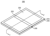
도 2는 본 발명의 다른 예시적인 실시예들에 따른 가요성 표시 장치를 설명하기 위한 사시도이다.
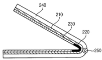
도 3 및 도 4는 도 1의 가요성 표시 장치가 동작하는 일 예를 나타내는 단면도들이다.
도 5 및 도 6은 도 2의 가요성 표시 장치가 동작하는 일 예를 나타내는 단면도들이다.
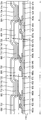
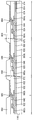
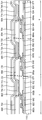
도 7은 도 1의 I-I' 라인 및 도 2의 Ⅱ-Ⅱ' 라인의 단면도이다.
도 8 내지 도 13은 본 발명의 예시적인 실시예들에 따른 가요성 표시 장치의 제조 방법을 설명하기 위한 단면도들이다.
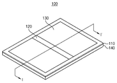
120, 220: 제1 표시 구조 130, 230: 제2 표시 구조
140, 240: 하우징 250: 힌지
620, 622, 624: 게이트 전극 630, 632, 634: 게이트 절연막
640, 642, 644: 활성층 650, 652, 654: 제1 층간 절연막
660a, 662a, 664a: 소스 전극 660b, 662b, 664b: 드레인 전극
670, 672, 674: 제2 층간 절연막 680, 682, 684: 제1 전극
690, 692, 694: 화소 정의막 700, 702, 704: 제1 유기층
710, 712, 714: 유기 발광층 720, 722, 724: 제2 유기층
730, 732, 734: 제2 전극 740, 742, 744: 상부 기판
Claims (20)
- 제1 표시 영역 및 제2 표시 영역을 구비하는 표시 영역 및 상기 표시 영역을 둘러싸는 주변 영역을 포함하는 가요성(flexible) 기판;
상기 기판의 제1 표시 영역 내에 위치하며, 나노 입자를 포함하는 제1 표시 구조(structure); 및
상기 기판의 제2 표시 영역 내에 위치하며, 실리콘을 포함하는 제2 표시 구조를 포함하는 가요성 표시 장치. - 제1항에 있어서, 상기 기판의 하부에 위치하고, 가요성 재질로 제조되며, 상기 가요성 표시 장치의 폴더블(foldable) 동작을 지지하는 하우징을 더 포함하는 것을 특징으로 하는 가요성 표시 장치.
- 제2항에 있어서, 상기 기판의 하부에 위치하고, 비가요성(non-flexible) 재질로 제조되며, 상기 가요성 표시 장치의 폴더블 동작을 지지하는 하우징을 더 포함하며, 상기 하우징은 상기 가요성 표시 장치의 폴더블 동작을 지지하기 위한 힌지(hinge)를 구비하는 것을 특징으로 하는 가요성 표시 장치.
- 제1항에 있어서, 상기 제1 표시 영역 및 상기 제2 표시 영역은 상기 기판 상에 연속적으로 배치되며, 상기 제2 표시 영역은 상기 제1 표시 영역의 양측에 배치되는 것을 특징으로 하는 가요성 표시 장치.
- 제1항에 있어서, 상기 제1 표시 구조는,
상기 기판 상에 배치되는 스위칭 부재(element)들;
상기 스위칭 부재들과 전기적으로 연결되는 제1 전극;
상기 제1 전극 상에 배치되는 발광 구조; 및
상기 발광 구조 상에 배치되는 제2 전극을 포함하며,
상기 스위칭 부재들, 상기 제1 전극, 상기 발광 구조 및 상기 제2 전극 중에서 적어도 하나는 나노 입자를 포함하는 것을 특징으로 하는 가요성 표시 장치. - 제5항에 있어서, 상기 발광 구조는,
제1 유기층;
상기 제1 유기층 상에 배치되는 유기 발광층; 및
상기 유기 발광층 상에 배치되는 제2 유기층을 포함하며,
상기 제1 유기층, 상기 유기 발광층 및 상기 제2 유기층 중에서 적어도 하나는 나노 입자를 포함하는 것을 특징으로 하는 가요성 표시 장치. - 제6항에 있어서, 상기 제1 유기층은 정공 주입층 또는 정공 수송층을 포함하는 것을 특징으로 하는 가요성 표시 장치.
- 제7항에 있어서, 상기 제2 유기층은 전자 수송층 또는 전자 주입층을 포함하는 것을 특징으로 하는 가요성 표시 장치.
- 제1항에 있어서, 상기 나노 입자는 탄소 나노 튜브(Carbon Nano Tube: CNT), 양자점(quantum dot), 그래핀(grephene) 및 플러렌(fullerene, C60) 중에서 적어도 하나를 포함하는 것을 특징으로 하는 가요성 표시 장치.
- 제1항에 있어서, 상기 실리콘은 비정질 실리콘, 단결정 실리콘 및 다결정 실리콘 중에서 적어도 하나를 포함하는 것을 특징으로 하는 가요성 표시 장치.
- 제1 표시 영역 및 제2 표시 영역을 구비하는 표시 영역 및 상기 표시 영역을 둘러싸는 주변 영역을 포함하는 기판을 제공하는 단계;
상기 기판의 상기 제1 표시 영역 내에 나노 입자를 포함하는 제1 표시 구조를 형성하는 단계; 및
상기 기판의 상기 제2 표시 영역 내에 실리콘을 포함하는 제2 표시 구조를 형성하는 단계를 포함하는 가요성 표시 장치의 제조 방법. - 제11항에 있어서, 상기 가요성 표시 패널의 하부에 위치하고, 가요성 재질로 제조되며, 상기 가요성 표시 패널의 폴더블 동작을 지지하는 하우징을 형성하는 단계를 더 포함하는 것을 특징으로 하는 가요성 표시 장치의 제조 방법.
- 제12항에 있어서, 상기 가요성 표시 패널의 하부에 위치하고, 비가요성 재질로 제조되며, 상기 가요성 표시 패널의 폴더블 동작을 지지하는 하우징을 형성하는 단계를 더 포함하며, 상기 하우징은 상기 가요성 표시 패널의 폴더블 동작을 지지하기 위한 힌지를 구비하는 것을 특징으로 하는 가요성 표시 장치의 제조 방법.
- 제11항에 있어서, 상기 제1 표시 영역 및 상기 제2 표시 영역은 상기 기판 상에 연속적으로 배치되며, 상기 제2 표시 영역은 상기 제1 표시 영역의 양측에 배치되는 것을 특징으로 하는 가요성 표시 장치의 제조 방법.
- 제11항에 있어서, 상기 제1 표시 구조를 형성하는 단계는,
상기 기판 상에 스위칭 부재들을 형성하는 단계;
상기 스위칭 부재들과 전기적으로 연결되는 제1 전극을 형성하는 단계;
상기 제1 전극 상에 발광 구조를 형성하는 단계; 및
상기 발광 구조 상에 제2 전극을 형성하는 단계를 포함하며,
상기 스위칭 부재들, 상기 제1 전극, 상기 발광 구조 및 상기 제2 전극 중에서 적어도 하나는 나노 입자를 포함하는 것을 특징으로 하는 가요성 표시 장치의 제조 방법. - 제15항에 있어서, 상기 발광 구조를 형성하는 단계는,
제1 유기층을 형성하는 단계;
상기 제1 유기층 상에 유기 발광층을 형성하는 단계; 및
상기 유기 발광층 상에 제2 유기층을 형성하는 단계를 포함하며,
상기 제1 유기층, 상기 유기 발광층 및 상기 제2 유기층 중에서 적어도 하나는 나노 입자를 포함하는 것을 특징으로 하는 가요성 표시 장치의 제조 방법. - 제16항에 있어서, 상기 발광 구조를 형성하는 단계는 잉크젯(inkjet) 프린팅 공정, 스크린(screen) 프린팅 공정, 노즐(nozzle) 프린팅 공정, 스프레이(spray) 코팅 공정, 슬릿(slit) 코팅 공정, 바(bar) 코팅 공정 또는 스핀(spin) 코팅 공정을 포함하는 것을 특징으로 하는 가요성 표시 장치의 제조 방법.
- 제16항에 있어서, 상기 제1 유기층은 정공 주입층 또는 정공 수송층을 포함하고, 상기 제2 유기층은 전자 수송층 또는 전자 주입층을 포함하는 것을 특징으로 하는 가요성 표시 장치의 제조 방법.
- 제11항에 있어서, 상기 나노 입자는 탄소 나노 튜브(CNT), 양자점, 그래핀 및 플러렌(C60) 중에서 적어도 하나를 포함하는 것을 특징으로 하는 가요성 표시 장치의 제조 방법.
- 제11항에 있어서, 상기 실리콘은 비정질 실리콘, 단결정 실리콘 및 다결정 실리콘 중에서 적어도 하나를 포함하는 것을 특징으로 하는 가요성 표시 장치의 제조 방법.
Priority Applications (3)
| Application Number | Priority Date | Filing Date | Title |
|---|---|---|---|
| KR1020130061492A KR102078679B1 (ko) | 2013-05-30 | 2013-05-30 | 가요성 표시 장치 및 가요성 표시 장치의 제조 방법 |
| US14/069,344 US9178172B2 (en) | 2013-05-30 | 2013-10-31 | Flexible display device having first and second display regions |
| US14/869,556 US9608216B2 (en) | 2013-05-30 | 2015-09-29 | Flexible display device and method of manufacturing the same |
Applications Claiming Priority (1)
| Application Number | Priority Date | Filing Date | Title |
|---|---|---|---|
| KR1020130061492A KR102078679B1 (ko) | 2013-05-30 | 2013-05-30 | 가요성 표시 장치 및 가요성 표시 장치의 제조 방법 |
Publications (2)
| Publication Number | Publication Date |
|---|---|
| KR20140140742A true KR20140140742A (ko) | 2014-12-10 |
| KR102078679B1 KR102078679B1 (ko) | 2020-02-20 |
Family
ID=51984095
Family Applications (1)
| Application Number | Title | Priority Date | Filing Date |
|---|---|---|---|
| KR1020130061492A Active KR102078679B1 (ko) | 2013-05-30 | 2013-05-30 | 가요성 표시 장치 및 가요성 표시 장치의 제조 방법 |
Country Status (2)
| Country | Link |
|---|---|
| US (2) | US9178172B2 (ko) |
| KR (1) | KR102078679B1 (ko) |
Cited By (4)
| Publication number | Priority date | Publication date | Assignee | Title |
|---|---|---|---|---|
| KR20160090979A (ko) * | 2015-01-22 | 2016-08-02 | 삼성디스플레이 주식회사 | 유기 발광 표시 장치 |
| KR20180062249A (ko) * | 2016-11-30 | 2018-06-08 | 엘지디스플레이 주식회사 | 커버 윈도우 및 이를 포함하는 폴더블 표시장치 |
| KR102088807B1 (ko) * | 2019-08-05 | 2020-03-16 | 연세대학교 산학협력단 | 스트레처블 발광소재를 이용한 삼차원 촉각 디스플레이 장치 및 그 제조방법 |
| US10961364B2 (en) | 2015-12-10 | 2021-03-30 | Samsung Electronics Co., Ltd. | Cover window for protecting display panel, display device using same, and cover window manufacturing method |
Families Citing this family (20)
| Publication number | Priority date | Publication date | Assignee | Title |
|---|---|---|---|---|
| USD769209S1 (en) * | 2014-05-30 | 2016-10-18 | Lg Electronics Inc. | Cellular phone |
| USD767526S1 (en) * | 2014-06-09 | 2016-09-27 | Lg Electronics Inc. | Cellular phone |
| USD772225S1 (en) * | 2014-08-07 | 2016-11-22 | Samsung Electronics Co., Ltd. | Electronic device |
| USD796499S1 (en) * | 2014-11-26 | 2017-09-05 | Samsung Electronics Co., Ltd. | Electronic device |
| WO2016095138A1 (zh) * | 2014-12-17 | 2016-06-23 | 深圳市柔宇科技有限公司 | 电子装置 |
| JP6823927B2 (ja) | 2015-01-21 | 2021-02-03 | 株式会社半導体エネルギー研究所 | 表示システム |
| USD797070S1 (en) * | 2015-03-09 | 2017-09-12 | Lg Electronics Inc. | Mobile phone |
| USD814435S1 (en) | 2015-10-26 | 2018-04-03 | Lenovo (Beijing) Co., Ltd. | Flexible electronic device |
| USD814455S1 (en) * | 2015-10-26 | 2018-04-03 | Lenovo (Beijing) Co., Ltd. | Flexible electronic device |
| KR102505585B1 (ko) * | 2015-12-31 | 2023-03-02 | 엘지디스플레이 주식회사 | 유기 발광 표시 패널 및 유기 발광 표시 장치 |
| US11374184B2 (en) | 2016-09-08 | 2022-06-28 | Boe Technology Group Co., Ltd. | Flexible substrate and fabrication method thereof, and flexible display apparatus |
| CN106206945A (zh) * | 2016-09-08 | 2016-12-07 | 京东方科技集团股份有限公司 | 一种柔性基板及其制备方法、柔性显示装置 |
| CN106960913A (zh) * | 2017-03-31 | 2017-07-18 | 武汉华星光电技术有限公司 | 量子点发光二极管显示面板及其制备方法 |
| CN107104192B (zh) * | 2017-04-14 | 2019-02-26 | 深圳市华星光电半导体显示技术有限公司 | 量子点显示器件及其制造方法 |
| US11751444B2 (en) * | 2018-03-29 | 2023-09-05 | Sharp Kabushiki Kaisha | Display device |
| CN110797466A (zh) * | 2018-08-02 | 2020-02-14 | 中国科学院苏州纳米技术与纳米仿生研究所 | 电子传输层墨水及其制作方法和应用 |
| US11063098B2 (en) * | 2019-09-04 | 2021-07-13 | Shenzhen China Star Optoelectronics Semiconductor Display Technology Co., Ltd. | Method for fabricating display panel having carbon quantum dot layer |
| KR102904846B1 (ko) | 2020-07-02 | 2025-12-26 | 엘지디스플레이 주식회사 | 플렉시블 표시패널 |
| KR20220083909A (ko) | 2020-12-11 | 2022-06-21 | 삼성디스플레이 주식회사 | 표시 장치 |
| KR102876110B1 (ko) * | 2021-11-02 | 2025-10-27 | 삼성디스플레이 주식회사 | 표시 장치 |
Citations (2)
| Publication number | Priority date | Publication date | Assignee | Title |
|---|---|---|---|---|
| WO2009141903A1 (ja) * | 2008-05-21 | 2009-11-26 | パイオニア株式会社 | 有機発光素子 |
| KR20110098349A (ko) * | 2010-02-26 | 2011-09-01 | 삼성전자주식회사 | 접이식 터치 스크린 디스플레이 장치 |
Family Cites Families (17)
| Publication number | Priority date | Publication date | Assignee | Title |
|---|---|---|---|---|
| US7592239B2 (en) | 2003-04-30 | 2009-09-22 | Industry University Cooperation Foundation-Hanyang University | Flexible single-crystal film and method of manufacturing the same |
| KR100569202B1 (ko) | 2003-04-30 | 2006-04-07 | 한양대학교 산학협력단 | 가요성 전기 광학 장치 및 그 제조 방법 |
| KR100547237B1 (ko) | 2003-05-23 | 2006-01-26 | 한양대학교 산학협력단 | 단결정 가요성 필름 및 가요성 전기 광학 장치의 제조방법, 이를 제조하는 장치 |
| US7604843B1 (en) * | 2005-03-16 | 2009-10-20 | Nanosolar, Inc. | Metallic dispersion |
| KR20050104065A (ko) | 2004-04-28 | 2005-11-02 | (주)케이디티 | 가요성 평면 유기 발광 원 |
| EP1624333B1 (en) * | 2004-08-03 | 2017-05-03 | Semiconductor Energy Laboratory Co., Ltd. | Display device, manufacturing method thereof, and television set |
| CN102569342B (zh) * | 2004-12-06 | 2015-04-22 | 株式会社半导体能源研究所 | 显示装置 |
| JP2007086729A (ja) * | 2005-06-20 | 2007-04-05 | Fuji Xerox Co Ltd | 表示媒体、それを用いた表示素子及び表示方法 |
| US7732330B2 (en) * | 2005-06-30 | 2010-06-08 | Semiconductor Energy Laboratory Co., Ltd. | Semiconductor device and manufacturing method using an ink-jet method of the same |
| JP4996846B2 (ja) * | 2005-11-22 | 2012-08-08 | 株式会社日立製作所 | 電界効果トランジスタ及びその製造方法 |
| US8222116B2 (en) * | 2006-03-03 | 2012-07-17 | Semiconductor Energy Laboratory Co., Ltd. | Method for manufacturing semiconductor device |
| US20070247422A1 (en) * | 2006-03-30 | 2007-10-25 | Xuuk, Inc. | Interaction techniques for flexible displays |
| WO2008143636A1 (en) * | 2006-11-01 | 2008-11-27 | Wake Forest University | Solid state lighting compositions and systems |
| GB0702350D0 (en) * | 2007-02-07 | 2007-03-21 | Plastic Logic Ltd | Electronic reading devices |
| KR20100026655A (ko) * | 2008-09-01 | 2010-03-10 | 삼성모바일디스플레이주식회사 | 박막 증착용 마스크 및 이를 이용한 유기전계발광 소자의 제조방법 |
| JP5613590B2 (ja) * | 2011-02-23 | 2014-10-29 | パナソニック株式会社 | 有機elデバイス |
| US8896202B2 (en) * | 2012-02-28 | 2014-11-25 | Lg Electronics Inc. | Display device |
-
2013
- 2013-05-30 KR KR1020130061492A patent/KR102078679B1/ko active Active
- 2013-10-31 US US14/069,344 patent/US9178172B2/en active Active
-
2015
- 2015-09-29 US US14/869,556 patent/US9608216B2/en active Active
Patent Citations (2)
| Publication number | Priority date | Publication date | Assignee | Title |
|---|---|---|---|---|
| WO2009141903A1 (ja) * | 2008-05-21 | 2009-11-26 | パイオニア株式会社 | 有機発光素子 |
| KR20110098349A (ko) * | 2010-02-26 | 2011-09-01 | 삼성전자주식회사 | 접이식 터치 스크린 디스플레이 장치 |
Cited By (5)
| Publication number | Priority date | Publication date | Assignee | Title |
|---|---|---|---|---|
| KR20160090979A (ko) * | 2015-01-22 | 2016-08-02 | 삼성디스플레이 주식회사 | 유기 발광 표시 장치 |
| US10961364B2 (en) | 2015-12-10 | 2021-03-30 | Samsung Electronics Co., Ltd. | Cover window for protecting display panel, display device using same, and cover window manufacturing method |
| KR20180062249A (ko) * | 2016-11-30 | 2018-06-08 | 엘지디스플레이 주식회사 | 커버 윈도우 및 이를 포함하는 폴더블 표시장치 |
| KR102088807B1 (ko) * | 2019-08-05 | 2020-03-16 | 연세대학교 산학협력단 | 스트레처블 발광소재를 이용한 삼차원 촉각 디스플레이 장치 및 그 제조방법 |
| US11195886B2 (en) | 2019-08-05 | 2021-12-07 | Industry-Academic Cooperation Foundation, Yonsei University | Organic light emitting diode and three-dimensional tactile display apparatus using stretchable light-emitting material and manufacturing method thereof |
Also Published As
| Publication number | Publication date |
|---|---|
| US20160020417A1 (en) | 2016-01-21 |
| KR102078679B1 (ko) | 2020-02-20 |
| US9178172B2 (en) | 2015-11-03 |
| US9608216B2 (en) | 2017-03-28 |
| US20140353613A1 (en) | 2014-12-04 |
Similar Documents
| Publication | Publication Date | Title |
|---|---|---|
| KR102078679B1 (ko) | 가요성 표시 장치 및 가요성 표시 장치의 제조 방법 | |
| Ju et al. | Transparent active matrix organic light-emitting diode displays driven by nanowire transistor circuitry | |
| KR101941178B1 (ko) | 유기 발광 표시 장치 및 유기 발광 표시 장치의 제조 방법 | |
| TWI584457B (zh) | 有機發光顯示裝置與製造有機發光顯示裝置的方法 | |
| JP4504908B2 (ja) | 薄膜トランジスタ及びこれを採用した平板表示装置 | |
| JP4370283B2 (ja) | 有機薄膜トランジスタを利用した有機電界発光表示装置 | |
| US20180158888A1 (en) | Organic Light Emitting Device | |
| CN100570882C (zh) | 发光器件 | |
| US9214496B2 (en) | Transistor, display, and electric apparatus | |
| CN102224580A (zh) | 薄膜晶体管制造方法、薄膜晶体管以及电子装置 | |
| TWI283145B (en) | Organic light-emitting display device | |
| CN106952929A (zh) | 显示单元及其制造方法和电子设备 | |
| JP2011216840A (ja) | 有機発光表示装置 | |
| CN100479192C (zh) | 有机薄膜晶体管以及包含这种晶体管的平板显示器 | |
| KR20180081770A (ko) | 베젤리스 표시 장치 및 그 제조 방법 | |
| CN106775048A (zh) | 触摸感测单元 | |
| JP4455517B2 (ja) | 薄膜トランジスタの製造方法 | |
| CN100573955C (zh) | 有机薄膜晶体管 | |
| CN1988204B (zh) | 有机发光二极管及其制造方法及具有该二极管的有机发光二极管显示器 | |
| KR20090128235A (ko) | 유기 발광 표시 장치 | |
| CN1893108B (zh) | 平板显示装置及其制造方法 | |
| JP5250981B2 (ja) | 有機デバイスの製造方法並びに電子機器 | |
| JP4273182B2 (ja) | 有機電界発光表示装置の製造方法とそれによる表示装置 | |
| JP2013115098A (ja) | トランジスタ、トランジスタの製造方法、表示装置および電子機器 | |
| WO2020107170A1 (zh) | 有机发光二极管器件、显示面板及显示装置 |
Legal Events
| Date | Code | Title | Description |
|---|---|---|---|
| PA0109 | Patent application |
Patent event code: PA01091R01D Comment text: Patent Application Patent event date: 20130530 |
|
| PG1501 | Laying open of application | ||
| A201 | Request for examination | ||
| PA0201 | Request for examination |
Patent event code: PA02012R01D Patent event date: 20180529 Comment text: Request for Examination of Application Patent event code: PA02011R01I Patent event date: 20130530 Comment text: Patent Application |
|
| E902 | Notification of reason for refusal | ||
| PE0902 | Notice of grounds for rejection |
Comment text: Notification of reason for refusal Patent event date: 20190430 Patent event code: PE09021S01D |
|
| E701 | Decision to grant or registration of patent right | ||
| PE0701 | Decision of registration |
Patent event code: PE07011S01D Comment text: Decision to Grant Registration Patent event date: 20191126 |
|
| GRNT | Written decision to grant | ||
| PR0701 | Registration of establishment |
Comment text: Registration of Establishment Patent event date: 20200212 Patent event code: PR07011E01D |
|
| PR1002 | Payment of registration fee |
Payment date: 20200213 End annual number: 3 Start annual number: 1 |
|
| PG1601 | Publication of registration | ||
| PR1001 | Payment of annual fee |
Payment date: 20240125 Start annual number: 5 End annual number: 5 |
|
| PR1001 | Payment of annual fee |
Payment date: 20250122 Start annual number: 6 End annual number: 6 |