KR20140146005A - 자기 정류 rram 소자 - Google Patents
자기 정류 rram 소자 Download PDFInfo
- Publication number
- KR20140146005A KR20140146005A KR20140072198A KR20140072198A KR20140146005A KR 20140146005 A KR20140146005 A KR 20140146005A KR 20140072198 A KR20140072198 A KR 20140072198A KR 20140072198 A KR20140072198 A KR 20140072198A KR 20140146005 A KR20140146005 A KR 20140146005A
- Authority
- KR
- South Korea
- Prior art keywords
- layer
- stack
- dielectric
- tunnel
- dielectric layers
- Prior art date
- Legal status (The legal status is an assumption and is not a legal conclusion. Google has not performed a legal analysis and makes no representation as to the accuracy of the status listed.)
- Ceased
Links
Images



Classifications
-
- H—ELECTRICITY
- H10—SEMICONDUCTOR DEVICES; ELECTRIC SOLID-STATE DEVICES NOT OTHERWISE PROVIDED FOR
- H10B—ELECTRONIC MEMORY DEVICES
- H10B63/00—Resistance change memory devices, e.g. resistive RAM [ReRAM] devices
- H10B63/20—Resistance change memory devices, e.g. resistive RAM [ReRAM] devices comprising selection components having two electrodes, e.g. diodes
- H10B63/22—Resistance change memory devices, e.g. resistive RAM [ReRAM] devices comprising selection components having two electrodes, e.g. diodes of the metal-insulator-metal type
-
- H—ELECTRICITY
- H10—SEMICONDUCTOR DEVICES; ELECTRIC SOLID-STATE DEVICES NOT OTHERWISE PROVIDED FOR
- H10B—ELECTRONIC MEMORY DEVICES
- H10B53/00—Ferroelectric RAM [FeRAM] devices comprising ferroelectric memory capacitors
- H10B53/30—Ferroelectric RAM [FeRAM] devices comprising ferroelectric memory capacitors characterised by the memory core region
-
- G—PHYSICS
- G11—INFORMATION STORAGE
- G11C—STATIC STORES
- G11C13/00—Digital stores characterised by the use of storage elements not covered by groups G11C11/00, G11C23/00, or G11C25/00
- G11C13/0002—Digital stores characterised by the use of storage elements not covered by groups G11C11/00, G11C23/00, or G11C25/00 using resistive RAM [RRAM] elements
-
- H—ELECTRICITY
- H10—SEMICONDUCTOR DEVICES; ELECTRIC SOLID-STATE DEVICES NOT OTHERWISE PROVIDED FOR
- H10B—ELECTRONIC MEMORY DEVICES
- H10B53/00—Ferroelectric RAM [FeRAM] devices comprising ferroelectric memory capacitors
- H10B53/20—Ferroelectric RAM [FeRAM] devices comprising ferroelectric memory capacitors characterised by the three-dimensional [3D] arrangements, e.g. with cells on different height levels
-
- H—ELECTRICITY
- H10—SEMICONDUCTOR DEVICES; ELECTRIC SOLID-STATE DEVICES NOT OTHERWISE PROVIDED FOR
- H10N—ELECTRIC SOLID-STATE DEVICES NOT OTHERWISE PROVIDED FOR
- H10N70/00—Solid-state devices having no potential barriers, and specially adapted for rectifying, amplifying, oscillating or switching
- H10N70/20—Multistable switching devices, e.g. memristors
- H10N70/24—Multistable switching devices, e.g. memristors based on migration or redistribution of ionic species, e.g. anions, vacancies
-
- H—ELECTRICITY
- H10—SEMICONDUCTOR DEVICES; ELECTRIC SOLID-STATE DEVICES NOT OTHERWISE PROVIDED FOR
- H10N—ELECTRIC SOLID-STATE DEVICES NOT OTHERWISE PROVIDED FOR
- H10N70/00—Solid-state devices having no potential barriers, and specially adapted for rectifying, amplifying, oscillating or switching
- H10N70/801—Constructional details of multistable switching devices
-
- H—ELECTRICITY
- H10—SEMICONDUCTOR DEVICES; ELECTRIC SOLID-STATE DEVICES NOT OTHERWISE PROVIDED FOR
- H10N—ELECTRIC SOLID-STATE DEVICES NOT OTHERWISE PROVIDED FOR
- H10N70/00—Solid-state devices having no potential barriers, and specially adapted for rectifying, amplifying, oscillating or switching
- H10N70/801—Constructional details of multistable switching devices
- H10N70/821—Device geometry
- H10N70/826—Device geometry adapted for essentially vertical current flow, e.g. sandwich or pillar type devices
-
- H—ELECTRICITY
- H10—SEMICONDUCTOR DEVICES; ELECTRIC SOLID-STATE DEVICES NOT OTHERWISE PROVIDED FOR
- H10N—ELECTRIC SOLID-STATE DEVICES NOT OTHERWISE PROVIDED FOR
- H10N70/00—Solid-state devices having no potential barriers, and specially adapted for rectifying, amplifying, oscillating or switching
- H10N70/801—Constructional details of multistable switching devices
- H10N70/881—Switching materials
- H10N70/883—Oxides or nitrides
- H10N70/8833—Binary metal oxides, e.g. TaOx
Landscapes
- Semiconductor Memories (AREA)
Abstract
Description
도 1a는 본 발명의 제1실시형태에 따르는 메모리 셀을 개략적으로 도시한다.
도 1b는 본 발명의 제2실시형태에 따르는 메모리 셀을 개략적으로 도시한다.
도 1c는 본 발명의 제3실시형태에 따르는 메모리 셀을 개략적으로 도시한다.
도 2는 상이한 바이어스 조건 하에서 도 1a의 메모리 셀 실시형태의 밴드 다이어그램을 도시한다.
도 3은 상이한 바이어스 조건 하에서, 대칭적인 유전체 스택을 갖는 본 발명의 또 다른 실시형태에 따르는 메모리 셀의 밴드 다이어그램을 도시한다.
도 4는 본 발명의 실시형태에 따르는 메모리 셀의 어레이를 개략적으로 도시한다.
도 5는 본 발명의 실시형태에 따르는 양방향 정류 스택의 IV 특성을 선형 스케일로 도시한다.
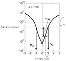
도 6은 도 5의 IV 특성을 로그 스케일로 도시한다.
도 7은 이중 유전체층을 갖는 본 발명의 제1실시형태에 따르는 2층 스택 터널 정류기/다이오드 및 삼중 유전체층을 갖는 본 발명의 또 다른 실시형태에 따르는 3층 스택 터널 정류기/다이오드의 단일층 터널 정류기 다이오드의 IV 특성을 도시한다.
도면은 개략적이고 비제한적이다. 도면에서, 일부 성분의 크기는 설명 목적으로 확대될 수 있고, 정확한 스케일로 그려진 것은 아니다. 치수 및 상대적인 치수는 본 발명을 실시하기 위해서 반드시 실제의 축소를 수반하는 것은 아니다.
청구범위에서 임의의 부호가 본 발명의 범위를 한정하는 것은 아니다.
상이한 도면에서, 동일한 부호는 동일한 또는 유사한 성분을 의미한다.


Claims (16)
- 전도체 물질 또는 반도체 물질로 제작된 제1전극 및 제2전극,
상기 제1전극과 상기 제2전극 사이의 저항 스위칭 소자,
상기 저항 스위칭 소자와 상기 제1전극 사이의 터널 정류기 - 상기 터널 정류기는 다층 터널 스택을 포함함 - 를 포함하고,
상기 다층 터널 스택은 각각 유전율(ki), 전도 밴드 오프셋(Φi), 및 두께에 의해서 정의된 적어도 2개의 유전체층의 스택(14)을 포함하고,
상기 다층 터널 스택에서 상기 유전체층 중 하나는 다른 유전체층보다 높은 유전율, 낮은 전도 밴드 오프셋, 및 높은 두께를 갖는, 메모리 셀.
- 제1항에 있어서,
상기 메모리 셀은 바이폴라 메모리 셀인, 메모리 셀
- 제1항에 있어서,
상기 다층 터널 스택은 적어도 3개의 유전체층의 스택이고, 제1 및 제2의 인접하는 유전체층 사이에 개재된 유전체층은 상기 제1 및 제2의 인접하는 유전체층보다 평균적으로 높은 유전율 (k2 > k1 및 k2> k3), 상기 제1 및 제2의 인접하는 유전체층보다 평균적으로 낮은 전도 밴드 오프셋(Φ2<Φ1 및 Φ2<Φ3), 및 상기 제1 및 제2의 인접하는 유전체층보다 높은 두께를 갖는, 메모리 셀.
- 제3항에 있어서,
상기 제1 및 제2의 인접하는 유전체층은 실질적으로 유사한 전도 밴드 오프셋을 갖는, 메모리 셀.
- 제3항에 있어서,
상기 제1 및 제2의 인접하는 유전체층의 유전율(k1, k3) 대 상기 제1 및 제2의 인접하는 유전체층 사이에 개재된 상기 유전체층의 유전율(k2)의 비율은 적어도 2인, 메모리 셀.
- 제3항에 있어서,
상기 다층 터널 스택(14)은 3개의 유전체층의 스택으로 이루어진, 메모리 셀.
- 제3항에 있어서,
상기 제1의 인접하는 유전체층은 상기 제1전극에 직접 접촉하는, 메모리 셀.
- 제3항에 있어서,
상기 다층 터널 스택은 대칭 또는 거의 대칭 스택인, 메모리 셀.
- 제3항에 있어서,
상기 다층 터널 스택은 비대칭 스택인, 메모리 셀.
- 제1항에 있어서,
상기 다층 터널 스택의 유전체층은 상기 저항 스위칭 소자에 직접 접촉하거나 상기 저항 스위칭 소자에 접촉하는 내부 전도층에 직접 접촉하는, 메모리 셀.
- 제10항에 있어서,
상기 내부 전도층은, 저항 스위칭에 기인하는 종들의 침투에 확산 베리어로서 작용하도록 적용되는, 메모리 셀.
- 제1항에 있어서,
상기 다층 터널 스택 중 적어도 하나의 유전체층은, 저항 스위칭에 기인하는 종들의 침투에 대한 우수한 확산 배리어의 물질로 사용되는, 메모리 셀.
- 제1항에 있어서,
상기 저항 스위칭 소자는 활성 유전체층 및 반응성 금속 캡층을 포함하는, 메모리 셀.
- 제1항에 있어서,
상기 저항 스위칭 소자가 형성되지 않는, 메모리 셀.
- 제1항에 있어서,
상기 저항 스위칭 소자는 공간적으로 국소 영역에 걸쳐서 상기 소자의 저항을 변화시킬 수 있는, 메모리 셀.
- 제1항에 있어서,
상기 높은 유전율 및 상기 낮은 전도 밴드 오프셋을 갖는 상기 유전체층의 두께는 1.8 nm 내지 3.5 nm인, 메모리 셀.
Applications Claiming Priority (2)
| Application Number | Priority Date | Filing Date | Title |
|---|---|---|---|
| EP13172187.0 | 2013-06-14 | ||
| EP13172187.0A EP2814073B1 (en) | 2013-06-14 | 2013-06-14 | Self-rectifying RRAM element |
Publications (1)
| Publication Number | Publication Date |
|---|---|
| KR20140146005A true KR20140146005A (ko) | 2014-12-24 |
Family
ID=48625898
Family Applications (1)
| Application Number | Title | Priority Date | Filing Date |
|---|---|---|---|
| KR20140072198A Ceased KR20140146005A (ko) | 2013-06-14 | 2014-06-13 | 자기 정류 rram 소자 |
Country Status (3)
| Country | Link |
|---|---|
| US (1) | US9595668B2 (ko) |
| EP (1) | EP2814073B1 (ko) |
| KR (1) | KR20140146005A (ko) |
Families Citing this family (22)
| Publication number | Priority date | Publication date | Assignee | Title |
|---|---|---|---|---|
| KR102244116B1 (ko) * | 2014-09-25 | 2021-04-26 | 인텔 코포레이션 | 장벽 층을 포함하는 1s1r 메모리 셀 |
| US10074694B2 (en) | 2015-07-24 | 2018-09-11 | Toshiba Memory Corporation | Memory device and method for manufacturing the same |
| US9899450B2 (en) | 2015-09-15 | 2018-02-20 | The Regents Of The University Of California | Memristors and method for fabricating memristors |
| KR102410947B1 (ko) | 2015-11-20 | 2022-06-22 | 에스케이하이닉스 주식회사 | 문턱 스위칭 장치 및 이를 포함하는 전자 장치 |
| CN105336852B (zh) * | 2015-12-10 | 2018-05-01 | 上海交通大学 | 带有自整流效应的rram存储单元结构及其制备方法 |
| KR102450814B1 (ko) | 2015-12-29 | 2022-10-05 | 에스케이하이닉스 주식회사 | 문턱 스위칭 장치 및 그 제조 방법과, 이를 포함하는 전자 장치 |
| KR102464205B1 (ko) | 2015-12-29 | 2022-11-09 | 에스케이하이닉스 주식회사 | 문턱 스위칭 장치 및 이를 포함하는 전자 장치 |
| US11041764B2 (en) * | 2016-02-29 | 2021-06-22 | Washington University | Self-powered sensors for long-term monitoring |
| CN105895800B (zh) * | 2016-04-21 | 2019-03-15 | 中国科学院微电子研究所 | 一种双极型阻变存储器及其制备方法 |
| US10157667B2 (en) | 2017-04-28 | 2018-12-18 | Micron Technology, Inc. | Mixed cross point memory |
| US10516105B2 (en) * | 2017-08-22 | 2019-12-24 | Sandisk Technologies Llc | Resistive memory device containing oxygen-modulated hafnium oxide material and methods of making thereof |
| CN108899418B (zh) * | 2018-07-09 | 2022-02-15 | 广东工业大学 | 一种非晶薄膜器件及其制备方法和应用 |
| US10985212B2 (en) * | 2019-04-16 | 2021-04-20 | Micron Technology, Inc. | Multi-component cell architectures for a memory device |
| JP2021048159A (ja) * | 2019-09-17 | 2021-03-25 | キオクシア株式会社 | 半導体記憶装置 |
| US11696521B2 (en) * | 2019-10-30 | 2023-07-04 | Taiwan Semiconductor Manufacturing Company, Ltd. | High electron affinity dielectric layer to improve cycling |
| US11482571B2 (en) * | 2020-06-23 | 2022-10-25 | Taiwan Semiconductor Manufacturing Company, Ltd. | Memory array with asymmetric bit-line architecture |
| US11997936B2 (en) * | 2020-09-02 | 2024-05-28 | Applied Materials, Inc. | Optimized selector and memory element with electron barrier |
| US20220138544A1 (en) * | 2020-10-30 | 2022-05-05 | Applied Materials, Inc. | Crested barrier device enhanced with interface switching modulation |
| CN113241404B (zh) * | 2021-03-29 | 2023-05-23 | 天津理工大学 | 基于二维氧化钼/硫化钼叠层结构的自选通器件及其制造方法 |
| CN113206194B (zh) * | 2021-04-30 | 2023-07-04 | 华中科技大学 | 一种自整流忆阻器、制备方法及其应用 |
| US12386917B2 (en) | 2021-08-16 | 2025-08-12 | Washington University | Multi-modal sensing blockchains using Fowler-Nordheim sensor data logger |
| US11996145B2 (en) * | 2022-05-03 | 2024-05-28 | Western Digital Technologies, Inc. | Cross-point array with threshold switching selector memory element |
Family Cites Families (20)
| Publication number | Priority date | Publication date | Assignee | Title |
|---|---|---|---|---|
| US5189503A (en) * | 1988-03-04 | 1993-02-23 | Kabushiki Kaisha Toshiba | High dielectric capacitor having low current leakage |
| US7507629B2 (en) * | 2004-09-10 | 2009-03-24 | Gerald Lucovsky | Semiconductor devices having an interfacial dielectric layer and related methods |
| KR100809724B1 (ko) | 2007-03-02 | 2008-03-06 | 삼성전자주식회사 | 터널링층을 구비한 바이폴라 스위칭 타입의 비휘발성메모리소자 |
| JP5198146B2 (ja) | 2008-05-22 | 2013-05-15 | 株式会社東芝 | 不揮発性記憶装置 |
| US8134194B2 (en) | 2008-05-22 | 2012-03-13 | Micron Technology, Inc. | Memory cells, memory cell constructions, and memory cell programming methods |
| US7936580B2 (en) * | 2008-10-20 | 2011-05-03 | Seagate Technology Llc | MRAM diode array and access method |
| KR101526926B1 (ko) * | 2008-12-30 | 2015-06-10 | 삼성전자주식회사 | 저항 메모리 소자 및 그 제조 방법 |
| JP5388710B2 (ja) | 2009-06-12 | 2014-01-15 | 株式会社東芝 | 抵抗変化メモリ |
| JP5558090B2 (ja) | 2009-12-16 | 2014-07-23 | 株式会社東芝 | 抵抗変化型メモリセルアレイ |
| US8351241B2 (en) | 2010-06-24 | 2013-01-08 | The Regents Of The University Of Michigan | Rectification element and method for resistive switching for non volatile memory device |
| US8901527B2 (en) * | 2010-07-02 | 2014-12-02 | Nanya Technology Corp. | Resistive random access memory structure with tri-layer resistive stack |
| KR101145332B1 (ko) * | 2010-09-17 | 2012-05-14 | 에스케이하이닉스 주식회사 | 스위칭 장치 및 이를 구비한 메모리 장치 |
| US8351242B2 (en) * | 2010-09-29 | 2013-01-08 | Micron Technology, Inc. | Electronic devices, memory devices and memory arrays |
| US8847196B2 (en) * | 2011-05-17 | 2014-09-30 | Micron Technology, Inc. | Resistive memory cell |
| US8853099B2 (en) * | 2011-12-16 | 2014-10-07 | Intermolecular, Inc. | Nonvolatile resistive memory element with a metal nitride containing switching layer |
| US20130277766A1 (en) * | 2012-04-23 | 2013-10-24 | Globalfoundries Inc. | Multiple high-k metal gate stacks in a field effect transistor |
| KR101929941B1 (ko) * | 2012-08-10 | 2018-12-18 | 삼성전자 주식회사 | 저항 변화 물질 소자 및 이를 적용한 디바이스 |
| US8766234B1 (en) * | 2012-12-27 | 2014-07-01 | Intermolecular, Inc. | Current selector for non-volatile memory in a cross bar array based on defect and band engineering metal-dielectric-metal stacks |
| US9147736B2 (en) * | 2013-03-01 | 2015-09-29 | Taiwan Semiconductor Manufacturing Company, Ltd. | High-K film apparatus and method |
| US9293196B2 (en) * | 2013-03-15 | 2016-03-22 | Micron Technology, Inc. | Memory cells, memory systems, and memory programming methods |
-
2013
- 2013-06-14 EP EP13172187.0A patent/EP2814073B1/en not_active Not-in-force
-
2014
- 2014-06-13 KR KR20140072198A patent/KR20140146005A/ko not_active Ceased
- 2014-06-16 US US14/306,116 patent/US9595668B2/en not_active Expired - Fee Related
Also Published As
| Publication number | Publication date |
|---|---|
| EP2814073A1 (en) | 2014-12-17 |
| US20140367631A1 (en) | 2014-12-18 |
| EP2814073B1 (en) | 2017-02-15 |
| US9595668B2 (en) | 2017-03-14 |
Similar Documents
| Publication | Publication Date | Title |
|---|---|---|
| KR20140146005A (ko) | 자기 정류 rram 소자 | |
| KR102796866B1 (ko) | 가변 저항 메모리 소자 | |
| US8445881B2 (en) | Nonvolatile variable resistive element and nonvolatile semiconductor memory device | |
| US8450709B2 (en) | Nonvolatile resistance change device | |
| KR102796867B1 (ko) | 가변 저항 메모리 소자 | |
| US9029187B1 (en) | Using multi-layer MIMCAPs with defective barrier layers as selector element for a cross bar memory array | |
| US8304754B2 (en) | Metal oxide materials and electrodes for Re-RAM | |
| US9324944B2 (en) | Selection device and nonvolatile memory cell including the same and method of fabricating the same | |
| JP6230229B2 (ja) | 集積トランジスタセレクタを有する積層rram | |
| US20130170283A1 (en) | Low forming voltage non-volatile storage device | |
| KR101457812B1 (ko) | 양방향 스위칭 특성을 갖는 2-단자 스위칭 소자, 이의 제조방법 및 이를 포함하는 저항성 메모리 소자 크로스-포인트 어레이 | |
| US9799706B2 (en) | Resistive random access memory device embedding tunnel insulating layer and memory array using the same and fabrication method thereof | |
| US8760920B2 (en) | Semiconductor memory device integrating flash memory and resistive/magnetic memory | |
| KR20130036279A (ko) | 저항-스위칭 층들 및 측면 배치를 구비한 메모리 셀 | |
| KR20070090328A (ko) | 비휘발성 메모리 소자 및 이를 포함하는 메모리 어레이 | |
| KR102871500B1 (ko) | 가변 저항 메모리 소자 | |
| US8471325B2 (en) | Nonvolatile memory device and method for manufacturing the same | |
| US10026896B2 (en) | Multilayered memristors | |
| US20150137062A1 (en) | Mimcaps with quantum wells as selector elements for crossbar memory arrays | |
| US10084015B2 (en) | Resistive memory element employing electron density modulation and structural relaxation | |
| US9036399B2 (en) | Variable resistance memory device | |
| KR101481920B1 (ko) | 금속-절연체 전이현상을 이용한 선택 소자, 및 이를 포함하는 비휘발성 메모리 셀 | |
| US11856879B2 (en) | MIEC and tunnel-based selectors with improved rectification characteristics and tunability |
Legal Events
| Date | Code | Title | Description |
|---|---|---|---|
| PA0109 | Patent application |
Patent event code: PA01091R01D Comment text: Patent Application Patent event date: 20140613 |
|
| PG1501 | Laying open of application | ||
| A201 | Request for examination | ||
| PA0201 | Request for examination |
Patent event code: PA02012R01D Patent event date: 20190514 Comment text: Request for Examination of Application Patent event code: PA02011R01I Patent event date: 20140613 Comment text: Patent Application |
|
| E902 | Notification of reason for refusal | ||
| PE0902 | Notice of grounds for rejection |
Comment text: Notification of reason for refusal Patent event date: 20200330 Patent event code: PE09021S01D |
|
| E601 | Decision to refuse application | ||
| PE0601 | Decision on rejection of patent |
Patent event date: 20200629 Comment text: Decision to Refuse Application Patent event code: PE06012S01D Patent event date: 20200330 Comment text: Notification of reason for refusal Patent event code: PE06011S01I |