KR20150004792A - Capacitive pressure sensor and a method of fabricating the same - Google Patents
Capacitive pressure sensor and a method of fabricating the same Download PDFInfo
- Publication number
- KR20150004792A KR20150004792A KR20147024444A KR20147024444A KR20150004792A KR 20150004792 A KR20150004792 A KR 20150004792A KR 20147024444 A KR20147024444 A KR 20147024444A KR 20147024444 A KR20147024444 A KR 20147024444A KR 20150004792 A KR20150004792 A KR 20150004792A
- Authority
- KR
- South Korea
- Prior art keywords
- layer
- diaphragm
- electrode plate
- pressure sensor
- forming
- Prior art date
- Legal status (The legal status is an assumption and is not a legal conclusion. Google has not performed a legal analysis and makes no representation as to the accuracy of the status listed.)
- Withdrawn
Links
Images











Classifications
-
- G—PHYSICS
- G01—MEASURING; TESTING
- G01L—MEASURING FORCE, STRESS, TORQUE, WORK, MECHANICAL POWER, MECHANICAL EFFICIENCY, OR FLUID PRESSURE
- G01L1/00—Measuring force or stress, in general
- G01L1/14—Measuring force or stress, in general by measuring variations in capacitance or inductance of electrical elements, e.g. by measuring variations of frequency of electrical oscillators
- G01L1/142—Measuring force or stress, in general by measuring variations in capacitance or inductance of electrical elements, e.g. by measuring variations of frequency of electrical oscillators using capacitors
- G01L1/148—Measuring force or stress, in general by measuring variations in capacitance or inductance of electrical elements, e.g. by measuring variations of frequency of electrical oscillators using capacitors using semiconductive material, e.g. silicon
-
- G—PHYSICS
- G01—MEASURING; TESTING
- G01L—MEASURING FORCE, STRESS, TORQUE, WORK, MECHANICAL POWER, MECHANICAL EFFICIENCY, OR FLUID PRESSURE
- G01L9/00—Measuring steady of quasi-steady pressure of fluid or fluent solid material by electric or magnetic pressure-sensitive elements; Transmitting or indicating the displacement of mechanical pressure-sensitive elements, used to measure the steady or quasi-steady pressure of a fluid or fluent solid material, by electric or magnetic means
- G01L9/0041—Transmitting or indicating the displacement of flexible diaphragms
- G01L9/0042—Constructional details associated with semiconductive diaphragm sensors, e.g. etching, or constructional details of non-semiconductive diaphragms
- G01L9/0048—Details about the mounting of the diaphragm to its support or about the diaphragm edges, e.g. notches, round shapes for stress relief
-
- B—PERFORMING OPERATIONS; TRANSPORTING
- B81—MICROSTRUCTURAL TECHNOLOGY
- B81C—PROCESSES OR APPARATUS SPECIALLY ADAPTED FOR THE MANUFACTURE OR TREATMENT OF MICROSTRUCTURAL DEVICES OR SYSTEMS
- B81C1/00—Manufacture or treatment of devices or systems in or on a substrate
- B81C1/00015—Manufacture or treatment of devices or systems in or on a substrate for manufacturing microsystems
- B81C1/00134—Manufacture or treatment of devices or systems in or on a substrate for manufacturing microsystems comprising flexible or deformable structures
- B81C1/00182—Arrangements of deformable or non-deformable structures, e.g. membrane and cavity for use in a transducer
-
- B—PERFORMING OPERATIONS; TRANSPORTING
- B81—MICROSTRUCTURAL TECHNOLOGY
- B81C—PROCESSES OR APPARATUS SPECIALLY ADAPTED FOR THE MANUFACTURE OR TREATMENT OF MICROSTRUCTURAL DEVICES OR SYSTEMS
- B81C1/00—Manufacture or treatment of devices or systems in or on a substrate
- B81C1/00436—Shaping materials, i.e. techniques for structuring the substrate or the layers on the substrate
- B81C1/00555—Achieving a desired geometry, i.e. controlling etch rates, anisotropy or selectivity
- B81C1/00626—Processes for achieving a desired geometry not provided for in groups B81C1/00563 - B81C1/00619
-
- G—PHYSICS
- G01—MEASURING; TESTING
- G01L—MEASURING FORCE, STRESS, TORQUE, WORK, MECHANICAL POWER, MECHANICAL EFFICIENCY, OR FLUID PRESSURE
- G01L19/00—Details of, or accessories for, apparatus for measuring steady or quasi-steady pressure of a fluent medium insofar as such details or accessories are not special to particular types of pressure gauges
- G01L19/06—Means for preventing overload or deleterious influence of the measured medium on the measuring device or vice versa
- G01L19/0618—Overload protection
-
- G—PHYSICS
- G01—MEASURING; TESTING
- G01L—MEASURING FORCE, STRESS, TORQUE, WORK, MECHANICAL POWER, MECHANICAL EFFICIENCY, OR FLUID PRESSURE
- G01L9/00—Measuring steady of quasi-steady pressure of fluid or fluent solid material by electric or magnetic pressure-sensitive elements; Transmitting or indicating the displacement of mechanical pressure-sensitive elements, used to measure the steady or quasi-steady pressure of a fluid or fluent solid material, by electric or magnetic means
- G01L9/0041—Transmitting or indicating the displacement of flexible diaphragms
- G01L9/0072—Transmitting or indicating the displacement of flexible diaphragms using variations in capacitance
- G01L9/0073—Transmitting or indicating the displacement of flexible diaphragms using variations in capacitance using a semiconductive diaphragm
-
- H—ELECTRICITY
- H04—ELECTRIC COMMUNICATION TECHNIQUE
- H04R—LOUDSPEAKERS, MICROPHONES, GRAMOPHONE PICK-UPS OR LIKE ACOUSTIC ELECTROMECHANICAL TRANSDUCERS; ELECTRIC HEARING AIDS; PUBLIC ADDRESS SYSTEMS
- H04R19/00—Electrostatic transducers
- H04R19/005—Electrostatic transducers using semiconductor materials
-
- H—ELECTRICITY
- H04—ELECTRIC COMMUNICATION TECHNIQUE
- H04R—LOUDSPEAKERS, MICROPHONES, GRAMOPHONE PICK-UPS OR LIKE ACOUSTIC ELECTROMECHANICAL TRANSDUCERS; ELECTRIC HEARING AIDS; PUBLIC ADDRESS SYSTEMS
- H04R31/00—Apparatus or processes specially adapted for the manufacture of transducers or diaphragms therefor
- H04R31/006—Interconnection of transducer parts
-
- B—PERFORMING OPERATIONS; TRANSPORTING
- B81—MICROSTRUCTURAL TECHNOLOGY
- B81B—MICROSTRUCTURAL DEVICES OR SYSTEMS, e.g. MICROMECHANICAL DEVICES
- B81B2201/00—Specific applications of microelectromechanical systems
- B81B2201/02—Sensors
- B81B2201/0264—Pressure sensors
-
- B—PERFORMING OPERATIONS; TRANSPORTING
- B81—MICROSTRUCTURAL TECHNOLOGY
- B81B—MICROSTRUCTURAL DEVICES OR SYSTEMS, e.g. MICROMECHANICAL DEVICES
- B81B2203/00—Basic microelectromechanical structures
- B81B2203/01—Suspended structures, i.e. structures allowing a movement
- B81B2203/0127—Diaphragms, i.e. structures separating two media that can control the passage from one medium to another; Membranes, i.e. diaphragms with filtering function
-
- H—ELECTRICITY
- H04—ELECTRIC COMMUNICATION TECHNIQUE
- H04R—LOUDSPEAKERS, MICROPHONES, GRAMOPHONE PICK-UPS OR LIKE ACOUSTIC ELECTROMECHANICAL TRANSDUCERS; ELECTRIC HEARING AIDS; PUBLIC ADDRESS SYSTEMS
- H04R19/00—Electrostatic transducers
- H04R19/04—Microphones
Landscapes
- Engineering & Computer Science (AREA)
- Physics & Mathematics (AREA)
- Manufacturing & Machinery (AREA)
- General Physics & Mathematics (AREA)
- Geometry (AREA)
- Microelectronics & Electronic Packaging (AREA)
- Acoustics & Sound (AREA)
- Signal Processing (AREA)
- Chemical & Material Sciences (AREA)
- Analytical Chemistry (AREA)
- Power Engineering (AREA)
- Measuring Fluid Pressure (AREA)
Abstract
본 발명은 정전용량형 압력센서 및 그 제조방법을 제시한다. 본 발명의 정전용량형 압력센서는 배면판으로 구성되는 고정극판, 압력을 감지하기 위한 다이아프램으로 구성되는 가동 극판, 상기 다이아프램의 변형을 허용하기 위하여 상기 고정극판과 가동극판 사이에 형성된 캐비티, 누설전류를 최소화하기 위한 상기 고정극판과 가동극판 사이의 절연층 및 그 전기접점들, 압력이 가해질 때 변형된 다이아프램과 같은 윤곽을 만들기 위하여 고정극판에 배열된 복수의 댐핑 홀, 주위 압력에 노출될 때 다이아프램에 평형을 제공하는 공기조정 통로를 가지는 상기 캐비티로 연장하는 벤트 홀, 및 정전용량형 압력 센서의 감도를 증대시키기 위한 확장된 용적을 갖는 확장된 배면실을 구비한다. 본 발명의 정전용량형 압력센서는 또한 기생정전용량을 극소화하는 구조로 된다. The present invention discloses a capacitive pressure sensor and a method of manufacturing the same. The capacitive pressure sensor of the present invention includes a fixed electrode plate composed of a back plate, a movable electrode plate composed of a diaphragm for sensing pressure, a cavity formed between the fixed electrode plate and the movable electrode plate to allow deformation of the diaphragm, An insulation layer between the fixed electrode plate and the movable electrode plate for minimizing the leakage current and its electrical contacts, a plurality of damping holes arranged in the fixed electrode plate to make a contour such as a deformed diaphragm when the pressure is applied, A vent hole extending into the cavity having an air conditioning passageway that provides an equilibrium in the diaphragm when the diaphragm is in contact with the diaphragm, and an extended back seal having an expanded volume for increasing the sensitivity of the capacitive pressure sensor. The capacitance type pressure sensor of the present invention also has a structure for minimizing the parasitic capacitance.
Description
본 발명은 일반적으로 압력센서에 관한 것이다. 특히, 본 발명은 정보획득 용도(acquisitic application)를 위한 정전용량형 압력 센서의 제조에 관한 것이다.The present invention relates generally to pressure sensors. In particular, the present invention relates to the fabrication of capacitive pressure sensors for acquisitive applications.
센서는 특정 매질을 감지하여 감지된 매질의 특성을 전기 신호를 통해 판독가능한 값으로 변환시키는 디바이스이다. 이러한 형태의 센서는 또한 변환기(tranducer)로 알려져 있다. 본 발명은 다양한 범위의 압력, 특히 수 파스칼 범위의 낮은 압력을 감지하기 위한 센서에 관한 것이다. A sensor is a device that detects a specific medium and converts the characteristics of the detected medium into a readable value through an electrical signal. This type of sensor is also known as a transducer. The present invention relates to a sensor for sensing a wide range of pressures, particularly low pressures in the range of a few pascals.
일반적으로 압력을 측정하는데 세가지 종류의 변환 메커니즘, 즉 피에조저항형(piezoresistive), 압전형(piezoelectric), 및 정전용량형(capacitive) 변환 메커니즘이 사용되고 있다. 그러나, 정전용량 방법은 다른 변환 메커니즘 보다 나은 장점, 특히 낮은 압력 측정에 장점이 있는데, 이는 압력에 대한 정전용량의 변화 백분율로 나타나는 것이다. In general, three types of conversion mechanisms are used to measure pressure: piezoresistive, piezoelectric, and capacitive conversion mechanisms. However, the capacitance method has advantages over other conversion mechanisms, especially for low pressure measurements, which is a percentage change in capacitance with respect to pressure.
그러나, 정전용량형 압력 센서의 대표적인 두 가지 단점은 커패시터의 극판들(plates) 사이의 누설전류(leakage current) 및 기생정전용량(parasitic capacitance)이다. 기생정전용량은 주정전용량 영역 외부의 주변 정전용량이다. 기생 정전용량은 병렬 극판들(parallel plates)이 각 극판의 전체 표면에서 부착되기 때문에 야기되는 것이다. 두 극판 사이의 누설전류는 정전용량을 악화시키며, 센서의 정밀도(resolution) 및 작동 주파수 범위를 저하시킨다. 따라서, 이와 같은 원치않는 두 가지의 파라미터들을 완전히 제거하거나 또는 크게 감소시켜, 센서 성능에 미치는 영향을 극소화하는 것이 요구된다. 상기 두 가지 파라미터가 영(0)인 것이 이상적이지만, 현재의 설계 및 제조 기술 상태에서, 적은 값이라도 항상 존재하고 있다. 그러므로, 상기한 점을 고려할 때, 전술한 단점들을 제거할 수 있고, 기생정전용량 및 누설전류가 극소화된 정전용량형 압력 센서를 생산할 수 있는 개선된 설계 및 제조 방법을 제공하는 것이 필요하다. However, two typical disadvantages of the capacitive pressure sensor are leakage current and parasitic capacitance between the plates of the capacitor. The parasitic capacitance is the perimeter capacitance outside the main capacitance area. Parasitic capacitance is caused by the fact that parallel plates are attached on the entire surface of each plate. Leakage current between the two plates worsens the capacitance and degrades the resolution and operating frequency range of the sensor. Therefore, it is required to completely eliminate or greatly reduce these two undesired parameters, thereby minimizing the impact on the sensor performance. Ideally, the two parameters are zero, but in the current design and manufacturing state, there is always a small value. Therefore, in view of the above, there is a need to provide an improved design and manufacturing method capable of eliminating the above-mentioned disadvantages and producing a capacitive pressure sensor with minimized parasitic capacitance and leakage current.
본 발명의 주된 목적은 기생정전용량 및 누설전류를 크게 감소시키는 특유의 설계 특성 및 제조 방법을 제공하는 것이다. SUMMARY OF THE INVENTION A primary object of the present invention is to provide unique design characteristics and fabrication methods that greatly reduce parasitic capacitance and leakage current.
본 발명의 또 하나의 목적은 간단한 방식으로 설계 요건들을 충족하는 초정전용량형(ultra capacitive) 압력 센서를 만드는 특유의 설계 및 제조 방법을 제공하는 것이다. It is another object of the present invention to provide a unique design and fabrication method of making an ultra capacitive pressure sensor that meets design requirements in a simple manner.
본 발명의 또 하나의 목적은 효율적인 코스트로 초정전용량형(ultra capacitive) 압력 센서를 만드는 특유의 설계 및 제조 방법을 제공하는 것이다. It is another object of the present invention to provide a unique design and fabrication method for creating an ultra capacitive pressure sensor at an efficient cost.
상기한 과제들을 해결하기 위하여, 본 발명은 센서 다이 상에 제조되는 정전용량형 압력 센서를 제공한다. 본 발명의 정전용량형 압력 센서는 기생정전용량을 최소화하기 위하여 엣지(edge)에서 앵커되고 나머지 영역은 뜬 상태(afloat)를 유지하는, 배면판(back plate)으로 구성되는 고정극판(fixed plate); 압력을 감지하기 위한 다이아프램(diaphragm)으로 구성되는 가동극판(movable plate), 상기 다이아프램의 변형(deflection)을 허용하기 위하여 상기 고정극판과 가동극판 사이에 형성된 캐비티(cavity); 누설전류를 최소화하기 위한 상기 고정극판과 가동극판 사이의 절연층 및 그 전기접점들; 압력이 가해질 때 변형된 다이아프램과 같은 윤곽을 만들기 위하여 고정극판에 배치된 복수의 댐핑 홀(damping hole); 주위 압력에 노출될 때 다이아프램에 평형을 제공하는 공기조정 통로(resistive air path)를 가지는 상기 캐비티로 연장하는 벤트 홀(vent hole); 및 정전용량형 압력 센서의 감도를 증대시키기 위한 확장된 용적을 갖는 확장된 배면실(extended back chamber)을 구비한다.In order to solve the above problems, the present invention provides a capacitive pressure sensor fabricated on a sensor die. The capacitance type pressure sensor of the present invention is a fixed plate composed of a back plate which is anchored at an edge and remains in an afloat in order to minimize parasitic capacitance. ; A movable plate composed of a diaphragm for sensing pressure; a cavity formed between the fixed electrode plate and the movable electrode plate to allow deflection of the diaphragm; An insulating layer between the fixed electrode plate and the movable electrode plate and their electrical contacts for minimizing leakage current; A plurality of damping holes disposed in the fixed electrode plate to produce a contour such as a deformed diaphragm when pressure is applied; A vent hole extending into the cavity having a resistive air path that provides balance to the diaphragm when exposed to ambient pressure; And an extended back chamber having an expanded volume for increasing the sensitivity of the capacitive pressure sensor.
하나의 구체예에서, 본 발명의 정전용량형 압력 센서는 다이아프램 상의 최대 과압의 경우에 상기 배면판 상에서 상기 다이아프램이 접히는 것을 방지하기 위하여 상기 고정극판에 배치된 복수의 과압 스토퍼 스터드(overpressure stopper stud)를 구비한다. In one embodiment, the capacitive pressure sensor of the present invention includes a plurality of overpressure stoppers disposed on the fixed electrode plate to prevent the diaphragm from folding on the back plate in case of maximum overpressure on the diaphragm. stud.
본 발명의 또 하나의 측면에서, 정전용량형 압력 센서를 제조하는 방법이 제시된다. 본 방법은 제1 접착제층에 의해 결합된 제1층 및 제2층과, 상기 제2층의 상부에 위치한 이산화규소재 마스킹층(masking layer)을 포함하여 구성되는 제1 웨이퍼 기판(wafer substrate)을 형성하는 단계; 상기 마스킹층과 상기 제2층을 에칭하여 오목형상의 캐비티를 형성하는 단계; 에칭에 의해 상기 마스킹층 상에 배면판, 전기절연(electrical isolation) 및 벤트채널(vent channel)을 위한 패턴을 형성하는 단계; 기생정전용량의 감소를 위한 배면판 절연 및 상기 제2층을 통한 댐핑 홀을 형성하는 단계; 하부에 제3 접착제층을 가지는 제3층과, 제4 접착제층에 의해 결합된 제4층을 포함하고, 상기 제4층이 통제 웨이퍼(constraint wafer)로 구성되는, 제2 웨이퍼 기판을 형성하는 단계; 제2 접착제층으로서 상기 마스킹층을 결합하는 것에 의해 상기 제1 웨이퍼 기판과 상기 제2 웨이퍼 기판을 커플링하는 단계; 그라인딩에 의해 상기 제4층을 10분의 1 마이크로미터 범위로 축소시켜 다이아프램의 층을 형성하는 단계; 감도 향상을 위하여 상기 제1층에 확장된 배면실(extended back chamber)를 형성하는 단계; 및 상기 다이아프램에 평형을 제공하기 위하여 상기 마스킹층에 벤트 홀을 위한 개구를 형성하는 단계를 포함한다. In another aspect of the present invention, a method of manufacturing a capacitive pressure sensor is presented. The method includes providing a first wafer substrate comprising a first layer and a second layer joined by a first adhesive layer and a masking layer of silicon dioxide located above the second layer, ; Etching the masking layer and the second layer to form a concave cavity; Forming a pattern for the back plate, electrical isolation and vent channel on the masking layer by etching; Forming a dummy hole through the second layer and a backplane insulation for reducing parasitic capacitance; A third layer having a third adhesive layer underneath, and a fourth layer bonded by a fourth adhesive layer, wherein the fourth layer is comprised of a constraint wafer, step; Coupling the first wafer substrate and the second wafer substrate by coupling the masking layer as a second adhesive layer; Reducing the fourth layer to a tenth of a micrometer range by grinding to form a layer of diaphragm; Forming an extended back chamber in the first layer for improved sensitivity; And forming an opening for the vent hole in the masking layer to provide an equilibrium in the diaphragm.
하나의 구체예에서, 본 발명의 정전용량형 압력 센서 제조방법은 불필요한 접착층들을 제거하여 상기 배면판과 상기 다이아프램을 유리(free)시키는 단계를 포함한다. In one embodiment, a method of manufacturing a capacitive pressure sensor of the present invention includes removing unnecessary adhesive layers to free the back plate and the diaphragm.
하나의 구체예에서, 본 발명의 정전용량형 압력 센서 제조방법은 접점 패드들(contact pads) 상에서 홀들(holes)을 통해 금속을 스퍼터링(sputtering)하는 단계를 포함한다. In one embodiment, a method of manufacturing a capacitive pressure sensor of the present invention comprises sputtering metal through holes on contact pads.
하나의 구체예에서, 상기 제1 웨이퍼 기판은 융착결합에 의해 상기 제2 웨이퍼 기판과 결합된다. In one embodiment, the first wafer substrate is bonded to the second wafer substrate by fusion bonding.
하나의 구체예에서, 상기 제1 층에서 확장된 배면실의 형성단계는, 확장된 배면실의 제1 단턱을 형성하는 단계; 및 확장된 배면실의 제2 단턱을 형성하여 상기 제1층에 완전한 배면실을 형성하는 단계를 포함한다. In one embodiment, the step of forming the extended back seal in the first layer comprises: forming a first step of the extended back seal; And forming a second step of the extended back seal to form a complete back seal in the first layer.
하나의 구체예에서, 본 발명의 정전용량형 압력 센서 제조방법은 상기 마스킹층을 앵커링 영역을 제외하고 엣지 둘레를 에칭하여 앵커링된 배면판을 형성하는 단계를 포함한다. In one embodiment, the method of manufacturing a capacitive pressure sensor of the present invention includes etching the masking layer to an edge, excluding the anchoring region, to form an anchored backing plate.
하나의 구체예에서, 본 발명의 정전용량형 압력 센서 제조방법은 최대 압력의 경우에 상기 배면판과 상기 다이아프램 사이에서 단락을 방지하기 위하여 상기 제2층을 통해 과압 스토퍼를 형성하는 단계를 포함한다. In one embodiment, the method of manufacturing a capacitive pressure sensor of the present invention includes forming an overpressure stopper through the second layer to prevent shorting between the back plate and the diaphragm in the case of maximum pressure do.
전술한 개략적인 설명과 후술하는 본 발명의 구체적인 실시예들의 상세한 설명은 청구되는 본 발명의 특성 및 특징을 이해하기 위한 개요 또는 골격을 제공하기 위한 것으로 이해되어야 한다. 첨부하는 도면들은 본 발명을 보다 잘 이해할 수 있도록 제공되는 것이며, 이들은 본 명세서에 통합되어 일부를 구성한다. 첨부 도면들은 본 발명의 여러 가지 구체적인 실시예들을 예시한 것으로 이에 관한 기술내용과 본 발명의 원리 및 작동을 설명한다. It is to be understood that both the foregoing general description and the following detailed description of specific embodiments of the present invention are provided to provide an overview or framework for understanding the nature and features of the invention as claimed. BRIEF DESCRIPTION OF THE DRAWINGS The accompanying drawings are included to provide a further understanding of the invention and are incorporated in and constitute a part of this specification. The accompanying drawings illustrate various specific embodiments of the invention and, together with the description, serve to explain the principles and operation of the invention.
본 발명의 전술한 특징과 장점 및 기타의 특징과 장점은 첨부도면에 예시된 본 발명의 실시예들을 참조하면 더 잘 이해되고 명백하게 될 것이다.
도 1은 전형적인 정전용량형 센서 모델을 예시한 것이고;
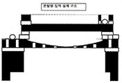
도 2a는 종래의 정전용량형 센서에서 극판의 설계 구조를 예시한 것이고;
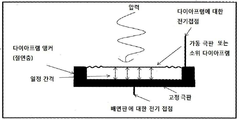
도 2b는 종래의 정전용량형 센서에서 압력이 감지될 때 극판이 아치형으로 변형하는 것을 예시한 것으로, 여기서 정전용량 영역의 특정부분이 변형된 스테이지에서 변하지 않고 유지되는 것을 보여주며;
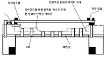
도 3a는 본 발명의 하나의 구체예에 따르는 정전용량형 센서의 특유한 캐비티 설계 구조를 예시한 것이고;
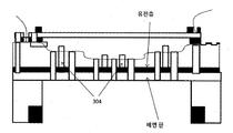
도 3b는 본 발명의 하나의 구체예에 따르는 과압 스토퍼 스터드를 예시한 것이고;
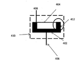
도 4는 본 발명의 하나의 구체예에 따르는 정전용량형 센서에서 기생정전용량의 형성을 예시한 것이고;
도 5는 본 발명의 하나의 구체예에 따라 기생정전용량을 감소시키기 위하여 두 극판의 절연(isolation)을 예시한 것이고;
도 6은 본 발명의 하나의 구체예에 따르는 정전용량형 센서에서 기생 및 구조 스트레스를 감소시키기 위하여 배면판을 떨어뜨리는 것을 예시한 것이고;
도 7은 정전용량형 센서에서 두 통로 사이의 누설 통로를 예시한 것이고;
도 8은 본 발명의 하나의 구체예에 따라 극판들 사이에서 단락에 의한 누설전류를 회피하기 위한 전기 절연을 예시한 것이고;
도 9는 본 발명의 하나의 구체예에 따르는 정전용량형 센서에서 캐비티를 향한 공기 조정 벤트구(air resistive vent)를 예시한 것이고;
도 10은 본 발명의 하나의 구체예에 따르는 정전용량형 센서에서 형성된 벤트 채널(vent channel)을 예시한 것이고;
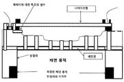
도 11은 본 발명의 하나의 구체예에 따르는 정전용량형 센서에서 확장된 배면 용적의 형성을 예시한 것이고;
도 12는 본 발명의 하나의 구체예에 따르는 정전용량형 센서의 평면도를 예시한 것이고;
도 13a 내지 도13o는 본 발명의 하나의 구체예에 따르는 정전용량형 센서의 특유한 제조 공정들을 예시한 것이고;
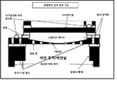
도 14는 본 발명의 하나의 구체예에 따르는 정전용량형 센서의 전체 설계구조를 예시한 것이고;
도 15는 본 발명의 또 하나의 구체예에 따라 앵커링 배면판을 가진 정전용량형 압력 센서의 설계구조를 예시한 것이고;
도 16a 내지 도 16b는 본 발명의 또 하나의 구체예에 따라 압력 스토퍼를 가진 정전용량형 압력 센서의 설계 구조를 예시한 것이다.The foregoing and other features and advantages of the present invention will become better understood and appreciated by reference to the embodiments of the invention illustrated in the accompanying drawings.
Figure 1 illustrates a typical capacitive sensor model;
2A illustrates a design structure of an electrode plate in a conventional capacitive sensor;
FIG. 2B illustrates arcuate deformation of the electrode plate when pressure is sensed in a conventional capacitive sensor, where a particular portion of the capacitance area remains unchanged in the modified stage;
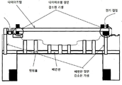
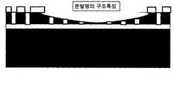
Figure 3a illustrates a unique cavity design structure of a capacitive sensor according to one embodiment of the present invention;
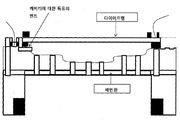
Figure 3b illustrates an overpressure stopper stud according to one embodiment of the present invention;
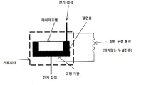
Figure 4 illustrates formation of parasitic capacitance in a capacitive sensor according to one embodiment of the present invention;
5 illustrates isolation of a bipolar plate to reduce parasitic capacitance according to one embodiment of the present invention;
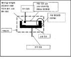
Figure 6 illustrates dropping the backplane to reduce parasitic and structural stress in a capacitive sensor according to one embodiment of the present invention;
Figure 7 illustrates a leakage path between two passages in a capacitive sensor;
Figure 8 illustrates electrical isolation to avoid leakage currents due to shorting between pole plates according to one embodiment of the present invention;
Figure 9 illustrates an air resistive vent from a capacitive sensor according to one embodiment of the present invention toward the cavity;
Figure 10 illustrates a vent channel formed in a capacitive sensor according to one embodiment of the present invention;
Figure 11 illustrates the formation of an expanded backside volume in a capacitive sensor according to one embodiment of the present invention;
Figure 12 illustrates a plan view of a capacitive sensor according to one embodiment of the present invention;
Figures 13A-13O illustrate specific fabrication processes of a capacitive sensor according to one embodiment of the present invention;
Figure 14 illustrates the overall design structure of a capacitive sensor according to one embodiment of the present invention;
15 illustrates a design structure of a capacitive pressure sensor having an anchoring back plate according to another embodiment of the present invention;
16A to 16B illustrate a design structure of a capacitive pressure sensor having a pressure stopper according to another embodiment of the present invention.
이하, 첨부하는 도면에 예시된 바와 같은 본 발명의 실시예들을 참조하여 설명하기로 한다. 가능한 한, 동일한 또는 유사한 부분들을 가리키는데 동일한 도면부호가 사용된다. Hereinafter, embodiments of the present invention will be described with reference to the accompanying drawings. Wherever possible, the same reference numbers will be used throughout the drawings to refer to the same or like parts.
여기서 설명되는 것은 기생정전용량 및 누설전류가 상대적으로 적은 정전용량형 압력 센서와, 이러한 초정전용량형 압력 센서의 제조방법이다. 도 1은 정전용량형 압력 센서의 전기 모델을 예시한 것이다. 전형적으로, 압력센서의 성능은 몇몇 주요특징에 의존한다. 이러한 특징의 예로는 높은 정전용량, 정전용량의 변화, 과압 보호, 최소의 기생정전용량, 최소의 누설전류, 낮은 주파수 감지를 세이프가드하는(safe guarding) 동안 캐비티의 대기압과 균등화, 확장된 배면 용적, 용적 가공 용이성(volume manufacturability) 및 코스트가 있다. 후술하는 본 발명 특유의 진보성은 본 발명의 압력센서에 우수한 성능과 매우 높은 상업적인 제품 구현가능성을 제공한다. Described here is a capacitive type pressure sensor having relatively small parasitic capacitance and leakage current, and a method of manufacturing such a super capacitive type pressure sensor. 1 illustrates an electrical model of a capacitive pressure sensor. Typically, the performance of the pressure sensor depends on several key features. Examples of such features include high capacitance, variation in capacitance, overpressure protection, minimum parasitic capacitance, minimum leakage current, equalization of the cavity during safe guarding of low frequency sensing, extended backing volume Volume manufacturability, and cost. The inventive features inherent in the present invention described below provide superior performance to pressure sensors of the present invention and very high commercial feasibility.
(1) 높은 정전용량 및 정전용량의 변화:(1) Change in high capacitance and capacitance:
커패시터의 두 극판은 기초재료로 단결정 실리콘을 사용하여 제조할 수 있다. 마이크로기계가공(micromachining)을 포함하는 표준 반도체(CMOS) 기술이 본 발명의 센서를 제조하는데 이용될 수 있다. The two electrode plates of the capacitor can be manufactured using monocrystalline silicon as a base material. Standard semiconductor (CMOS) techniques, including micromachining, can be used to fabricate the sensor of the present invention.
다이아프램에 인가되는 압력을 감지하기 위한 정전용량형 센서를 만들기 위하여, 캐비티 또는 공간(space)이 커패시터 극판들 사이에 형성된다. 따라서, 다이아프램은 압력이 가해질 때 구부러지고, 가해진 압력의 양은 정전용량의 변화로 나타난다. 종래의 설계에서, 정전용량형 센서의 두 극판은 도 2a에 나타낸 바에 따라 제조된다. 압력이 다이아프램에 가해지면, 상기 다이아프램은 전후로 진동하여, 정전용량 값이 정전용량형 압력 센서에서 변화한다. 다이아프램의 변형은 다이아프램 상에 감지된 압력의 양에 비례한다. 그러나, 종래의 설계는 단점이 하나 있다. 최대의 감도를 얻기 위하여, 다이아프램은 대향 극판(배면판) 위에 붕괴됨이 없이(without collapsing) 최대 수준으로 변형하여야 한다. 다이아프램이 변형할 때, 도 2b에 나타낸 바와 같이 아치형으로 구부러진다. 이 시점에서, 다이아프램 아래의 특정 영역들이 유의적으로 확장하지 않는다. 따라서, 극판들 사이의 간격이 거의 변하지 않아 정전용량의 변화에 기여하지 않는다. In order to create a capacitive sensor for sensing the pressure applied to the diaphragm, a cavity or space is formed between the capacitor plates. Therefore, the diaphragm is bent when pressure is applied, and the amount of applied pressure is indicated by the change in capacitance. In the conventional design, the two electrode plates of the capacitive sensor are manufactured as shown in Fig. 2A. When pressure is applied to the diaphragm, the diaphragm oscillates back and forth, and the capacitance value changes in the capacitive pressure sensor. The deformation of the diaphragm is proportional to the amount of pressure sensed on the diaphragm. However, the conventional design has one disadvantage. To obtain maximum sensitivity, the diaphragm must be deformed to its maximum level without collapsing on the opposite plate (back plate). When the diaphragm is deformed, it is bent in an arcuate shape as shown in Fig. 2B. At this point, certain areas under the diaphragm do not significantly expand. Therefore, the gap between the electrode plates is hardly changed and does not contribute to the change of the capacitance.
도 3에 나타낸 본 발명의 설계 구조는 압력이 다이아프램에 인가될 때, 변형된 다이아프램의 윤곽을 따르도록 정전용량 극판들 사이의 간격을 형성한다. 이는 도 3a에 나타낸 바와 같이 댐핑 홀(302)의 이용에 의해 달성된다. 이에 의해 정전용량의 최대 변화가 산출된다. The design structure of the present invention shown in Figure 3 forms the spacing between the electrostatic capacity plates to follow the contour of the deformed diaphragm when pressure is applied to the diaphragm. This is accomplished by the use of a damping
(2) 과압 보호(over-pressure protection):(2) Over-pressure protection:
본 발명의 제조 기술에서, 과압 스토퍼(304)가 캐비티의 내부를 형성하기 위해 사용된다. 다이아프램이 최대의 과압을 겪게 되면, 상기 과압 스토퍼 스터드들(304)은 다이아프램이 배면판 위에 붕괴되어 이 디바이스를 단락시키는 것을 방지하게 된다. 상기 과압 스토퍼 스터드들은 유전 층 상에 형성되어, 도 3b에 나타낸 바와 같이 전기 바이어스(electrical bias)에 접속되지 않는다. In the manufacturing technique of the present invention, the
(3) 감소된 기생정전용량:(3) Reduced parasitic capacitance:
전술한 바와 같이, 본 발명의 정전용량형 압력 센서는 두 개의 병렬 극판을 구비한다. 한 극판은 고정극판(402)이고, 다른 극판은 다이아프램(404)이라 칭해지는 가동 극판이다. 커패시터는 고정극판(402) 및 다이아프램(404)에 각각 연결되는 전기 접점들(electrical contacts)(406, 408)을 구비한다. 두 극판이 커패시터를 형성하도록 제조되면, 두 가지의 정전용량, 즉 액티브 정전용량(active capacitance)(410)과 패시브 정전용량(passive capacitance) (412)이 형성된다. 상기 패시브 정전용량은 기생정전용량이라 칭하기도 한다. 이는 두 극판이 결합된 도 4에 예시된다. 이러한 패시브 정전용량은 액티브 정전용량에 병렬로 형성되어, 센서 디바이스의 전체 성능을 저하시킨다. 따라서, 본 발명의 주된 과제는 상기한 기생정전용량을 제거하거나 또는 극소화하는 것이다. 본 발명 특유의 설계 및 제조방법은 기생정전용량을 전체 정전용량의 20% 보다 적게 줄이는 것을 가능하게 한다. As described above, the capacitive pressure sensor of the present invention has two parallel plates. One of the electrode plates is a fixed
본 발명의 방법은 도 5에 나타낸 바와 같이 고정극판과 다이아프램의 중첩 영역(superimposed area)을 절연시키는 것에 의해 기생정전용량을 감소시킨다. 이러한 설계에서, 하나의 옵션은 배면판을 유리상태(free)로 하는 것이다. 이를 위해, 배면판은 소형 빔으로 앵커되고, 나머지 영역은 뜬상태로 있다. 이는 도 6에 나타낸 바와 같이 기생정전용량을 극소화하여 구조적 스트레스를 감소시킨다. The method of the present invention reduces the parasitic capacitance by isolating the superimposed area of the diaphragm from the fixed electrode plate as shown in Fig. In this design, one option is to make the back plate free. To this end, the back plate is anchored with a small beam and the remaining area is floating. This minimizes the parasitic capacitance as shown in FIG. 6, thereby reducing the structural stress.
(4) 두 극판 사이의 누설전류:(4) Leakage current between two plates:
두 극판이 커패시터를 형성하도록 제조되면, 두 극판이 결합하여 형성된 영역도 있다. 이러한 영역이 소위 절연 영역(isolation area)이다. 그러나, 도 7에 나타낸 바와 같이 상기 디바이스에 전원이 연결되어 있는 동안, 두 극판 사이를 통해서 미량의 전류가 누설되는 경향이 있다. 디바이스 성능의 악화는 누설전류의 양에 좌우될 수 있다. 따라서, 장치 설계시 누설전류가 없게 하거나 최소가 되도록 하는데 상당한 주의를 요한다. When the two electrode plates are manufactured so as to form a capacitor, there are regions where the two electrode plates are combined. This area is a so-called isolation area. However, as shown in Fig. 7, while power is connected to the device, a minute amount of current tends to leak through between the two electrode plates. The deterioration of the device performance may depend on the amount of leakage current. Therefore, care must be taken to avoid or minimize leakage currents when designing the device.
본 발명의 설계 및 제조방법은 도 8에 예시한 바와 같이 누설전류를 최소화하는 것을 가능하게 한다. 본 발명에 따르는 특유한 방식으로 전기 접점 둘레의 영역을 절연하여, 두 극판 사이에서 단락이 없게 하는 것을 보장한다. 게다가, 배면판과 다이아프램을 특유한 방식으로 전체 둘레에서 절연하여, 두 극판 사이에서 단락이 없게 하는 것을 보장한다.The design and fabrication method of the present invention makes it possible to minimize the leakage current as illustrated in Fig. The area around the electrical contacts is insulated in a unique manner in accordance with the invention to ensure that there is no shorting between the two plates. In addition, the backplane and diaphragm are insulated from their entire perimeter in a unique manner, ensuring that there is no shorting between the two plates.
(5) 캐비티를 대기압에 통기하기 위한 특유의 벤트 형성:(5) Form a unique vent to vent the cavity to atmospheric pressure:
일부 압력센서는 게이지 용도로 사용되며, 이러한 게이지 용도에서 다이아프램은 도 9에 나타낸 바와 같이 양 사이드 상에서 동일한 주위 압력에 노출된다. 이를 다이아프램과 평형에 이르도록 하기 위하여, 벤트를 형성하여 캐비티를 노출시킨다. 그러나, 이러한 벤트는 입사압력(incident pressure)이, 특히 음향 압력(sound pressure)의 경우에, 다이아프램의 양 사이드에서 동시에 노출되지 않는 방식으로 설계되어 제조되어야 한다. Some pressure sensors are used for gauge applications where the diaphragm is exposed to the same ambient pressure on both sides as shown in Fig. A vent is formed to expose the cavity to achieve equilibration with the diaphragm. However, these vents must be manufactured in such a way that the incident pressure is not exposed at the same time on both sides of the diaphragm, especially in the case of sound pressure.
본 발명의 설계 및 제조 방법은 도 10에 예시한 바와 같이 캐비티로 들어오는 음파에 위상차(phase shift)를 일으키는 공기조정 통로를 만들면서, 상기 캐비티를 대기압에 노출시키는 벤트를 형성하는 것을 가능하게 한다. The design and fabrication method of the present invention makes it possible to form a vent that exposes the cavity to atmospheric pressure, while creating an air conditioning passageway that causes a phase shift in the sound waves entering the cavity as illustrated in FIG.
(6) 확장된 배면 용적:(6) Expanded backing volume:
상기 배면 용적은 센서의 집적부이다. 배면 용적이 클수록, 센서의 감지 성능도 양호하게 된다. 센서의 배면 용적을 증대시키기 위하여, 받침대(pedestal)의 일부가 에칭에 의해 제거된다. 본 발명의 설계 및 제조방법은 도 11에 나타낸 바와 같이 확장된 배면 용적의 형성을 가능하게 한다. The backside volume is an integral part of the sensor. The larger the backside volume, the better the sensing performance of the sensor. In order to increase the backside volume of the sensor, a part of the pedestal is removed by etching. The design and fabrication method of the present invention enables the formation of an extended backside volume as shown in FIG.
도 12는 본 발명의 하나의 구체예에 따르는 정전용량형 압력 센서의 전체 설계 구조의 평면도를 나타낸 것이다. 본 정전용량형 압력 센서 다이(1200)는 고정 배면판(1202), 가동 다이아프램(1204), 및 이들 사이의 캐비티(1206)을 구비한다. 전기접점들(1208 및 1210)이 상기 배면판과 상기 다아이프램에 각각 제공된다. 도면부호 1212는 전기접점 개구를 가리킨 것이다. 본 정전용량형 압력 센서(1200)는 또한 댐핑 홀(1214), 과압 스토퍼 스터드(1216), 및 다이아프램의 전기/기생 절연(1218)을 구비한다. 공기통로를 갖는 벤트 홀(1220)이 또한 도시되어 있다. 12 shows a top view of the overall design structure of a capacitive pressure sensor according to one embodiment of the present invention. The present capacitive pressure sensor die 1200 includes a fixed
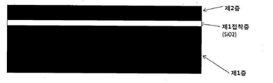
도 13a 내지 13o는 본 발명의 하나의 구체예에 따르는 압력센서의 제조공정들을 예시한 것이다. 전형적으로 제1층은 핸들/통제(handle/constraint) 웨이퍼를 포함한다. 이 구체예에서 배면판인 제2층은 제1 접착제층을 개재하여 제1층에 형성된다 (도 13a에 도시됨). 상기 제1접착제 층은 이산화규소층일 수 있다. Figures 13A-13O illustrate the manufacturing process of a pressure sensor according to one embodiment of the present invention. Typically, the first layer includes a handle / constraint wafer. In this embodiment, the second layer, which is the backing plate, is formed in the first layer via the first adhesive layer (shown in Fig. 13A). The first adhesive layer may be a silicon dioxide layer.
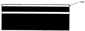
다음, 마스킹 층이 제2층의 상부에 형성된다. 예를 들어, 상기 마스킹층은 이산화규소층(Si02)일 수 있다 (도 13b에 도시됨).Next, a masking layer is formed on top of the second layer. For example, the masking layer may be a layer of silicon dioxide (Si0 2) (shown in Figure 13b).
다음, 이산화규소로 된 상기 마스킹층에 패턴이 형성되고, 제2층이 제거 또는 에칭 제거되어, 오목한 또는 스텝다운(step-down) 캐비티를 형성한다 (도 13c에 도시됨). Next, a pattern is formed on the masking layer of silicon dioxide and the second layer is removed or etched away to form a recessed or step-down cavity (shown in FIG. 13C).
다음, 상기 마스킹 층에 추가로 패턴이 형성되고, 배면판을 위하여 에칭된다 (도 13d에 도시됨). 이에 의해, 특유의 기생 축소를 위한 배면판 절연, 배면판 벤트 채널의 절연 및 댐핑 홀이 제2층을 통해 형성된다 (도 13e에 도시됨).Next, a pattern is further formed on the masking layer and etched for the backing plate (shown in FIG. 13D). Thereby, back plate insulation for unique parasitic reduction, insulation of back plate vent channels and damping holes are formed through the second layer (shown in FIG. 13E).
이 구체예에서 다이아프램인 제3층이 제4 접착제층을 개재하여 제4층에 형성된다 (도 13f에 도시됨). 제4층은 이 구체예에서 규소 또는 절연체(silicon or insulator: SOI) 웨이퍼일 수 있는 핸들 또는 통제 웨이퍼로서 작동한다. 상기 제4접착제층은 이산화규소일 수 있다. In this embodiment, a third layer, which is a diaphragm, is formed in the fourth layer via a fourth adhesive layer (shown in Figure 13F). The fourth layer acts as a handle or control wafer, which in this embodiment may be a silicon or insulator (SOI) wafer. The fourth adhesive layer may be silicon dioxide.
마스킹층을 제2 접착체층으로 사용하여, 두 세트를 함께 결합하고, 이 구체예에서는 융착을 사용하여 상기 두 세트를 함께 결합한다 (도 13g 및 13h에 도시됨).Using the masking layer as the second adhesive layer, the two sets are bonded together, and in this embodiment, the two sets are bonded together using fusing (shown in Figures 13g and 13h).
두 세트를 융착결합한 후에, 제4층을 그라인딩하여 10분의 1 마이크론까지 축소시킨다 (도 13i에 도시됨). After the two sets are fused together, the fourth layer is ground down to a tenth of a micron (shown in Figure 13i).
다음, 배면실 용적이 확장된다. 제1층에 배면실을 확장시키기 시작하여, 제1층에 완전한 배면실을 형성한다 (도 13j 및 13k에 도시됨).Next, the capacity of the back face room is expanded. Start to extend the backside seal to the first layer and form a complete backside seal in the first layer (shown in Figures 13j and 13k).
다음, 벤트 홀 및 결합 패드 개구(bond pad opening)를 형성한다(도13l에 도시됨). Next, a vent hole and a bond pad opening are formed (shown in FIG. 13L).
또한, 다이아프램, 전기절연, 기생축소, 및 결합 패드를 형성한다 (도13m에 도시됨). In addition, diaphragms, electrical isolation, parasitic reduction, and bonding pads are formed (shown in Figure 13m).
이어서, 불필요한 접착제층을 모두 제거하여, 극판들을 유리시킨다 (도13n에 도시됨). 그 후, 접점 패드 상에서 벤트 홀을 통해 금속을 스퍼터링한다(도 13o에 도시됨. Subsequently, all unnecessary adhesive layers are removed, and the electrode plates are released (shown in FIG. 13N). The metal is then sputtered through the vent holes on the contact pads (shown in Figure 13O).
도 14는 본 발명의 설계 특징들을 갖는 정전용량형 압력 센서의 측면도를 나타낸 것이다. Figure 14 shows a side view of a capacitive pressure sensor having design features of the present invention.
본 발명의 또 하나의 구체예에서, 정전용량형 압력 센서가 선택적인 앵커링 배면판을 구비할 수 있다. 댐핑 홀의 형성중에, 도 15도에 나타낸 바와 같은 앵커링 영역을 제외하고 상기 극판의 엣지 둘레를 에칭하기 위하여 마스크를 설계한다. 이는 절연 및 접착층이 제거될 때 상기 배면판이 뜬상태가 되는 것을 가능하게 한다. 그 기능이 댐핑 홀이 형성되는 경우와 같이, 동일한 마스크에서 지연되므로, 추가 단계를 필요로 하지 않는다. 또한 전술한 공정에 추가적인 변화가 없다. In another embodiment of the invention, the capacitive pressure sensor may comprise an optional anchoring back plate. During formation of the damping hole, the mask is designed to etch around the edge of the electrode plate except for the anchoring area as shown in FIG. 15. This makes it possible for the back plate to be in a floating state when the insulation and the adhesive layer are removed. The function is delayed in the same mask as in the case where the damping hole is formed, so that no additional step is required. There is also no further change to the process described above.
도 16a 내지 16b는 선택적인 과압 스토퍼를 포함하는 본 발명의 또 하나의 구체예에 따르는 정전용량형 압력 센서의 설계 및 제조방법을 예시한 것이다. 도 16a 내지 16b에서 나타낸 제조방법의 차이는 전기적으로 절연된 과압 스토퍼를 구비시킨 것이다. 16A-16B illustrate a method of designing and manufacturing a capacitive pressure sensor according to another embodiment of the present invention including an optional overpressure stopper. The difference in the manufacturing method shown in Figs. 16A to 16B is to provide an electrically insulated overpressure stopper.
당 분야의 통상의 기술을 가진 자는 본 발명의 범위 및 정신에서 벗어남이 없이 다양한 수정들 및 변경들을 만들어 낼 수 있음을 이해하여야 한다. 따라서, 첨부하는 청구항들 및 그 균등물들의 범위 내에 있는 한, 본 발명은 상기한 수정들 및 변경들을 망라하는 것으로 의도된 것이다.
It should be understood by those of ordinary skill in the art that various changes and modifications may be made without departing from the scope and spirit of the invention. Accordingly, it is intended that the present invention cover the modifications and variations that fall within the scope of the appended claims and their equivalents.
Claims (9)
기생정전용량을 최소화하기 위하여 엣지에서 앵커되고 나머지 영역은 뜬상태를 유지하는, 배면판으로 구성되는 고정극판;
압력을 감지하기 위한 다이아프램으로 구성되는 가동 극판;
상기 다이아프램의 변형을 허용하기 위하여 상기 고정극판과 가동극판 사이에 형성된 캐비티;
누설전류를 최소화하기 위한 상기 고정극판과 가동극판 사이의 절연층 및 그 전기접점들;
압력이 가해질 때 변형된 다이아프램과 같은 윤곽을 만들기 위하여 고정극판에 배치된 복수의 댐핑 홀;
주위 압력에 노출될 때 다이아프램에 평형을 제공하는 공기조정 통로를 가지는 상기 캐비티로 연장하는 벤트 홀; 및
정전용량형 압력 센서의 감도를 증대시키기 위한 확장된 용적을 갖는 확장된 배면실;을 포함하여 구성되는, 정전용량형 압력 센서.A capacitive pressure sensor fabricated on a sensor die,
A fixed electrode plate comprising a back plate anchored at the edge and remaining in a floating state to minimize parasitic capacitance;
A movable electrode plate composed of a diaphragm for sensing pressure;
A cavity formed between the fixed electrode plate and the movable electrode plate to allow deformation of the diaphragm;
An insulating layer between the fixed electrode plate and the movable electrode plate and their electrical contacts for minimizing leakage current;
A plurality of damping holes arranged in the fixed electrode plate to make a contour like a deformed diaphragm when pressure is applied;
A vent hole extending into the cavity having an air conditioning passageway that provides balance to the diaphragm when exposed to ambient pressure; And
And an expanded back seal having an expanded volume for increasing the sensitivity of the capacitive pressure sensor.
제1 접착제층에 의해 결합된 제1층 및 제2층과, 상기 제2층의 상부에 위치한 이산화규소재 마스킹층을 포함하여 구성되는 제1 웨이퍼 기판을 형성하는 단계;
상기 마스킹층과 상기 제2층을 에칭하여 오목형상의 캐비티를 형성하는 단계;
에칭에 의해 상기 마스킹층 상에 배면판, 전기절연 및 벤트채널을 위한 패턴을 형성하는 단계;
기생정전용량의 감소를 위한 배면판 절연 및 상기 제2층을 통한 댐핑 홀을 형성하는 단계;
하부에 제3 접착제층을 가지는 제3층과, 제4 접착제층에 의해 결합된 제4층을 포함하고, 상기 제4층이 통제 웨이퍼로 구성되는, 제2 웨이퍼 기판을 형성하는 단계;
제2 접착제층으로서 상기 마스킹층을 결합하는 것에 의해 상기 제1 웨이퍼 기판과 상기 제2 웨이퍼 기판을 커플링하는 단계;
그라인딩에 의해 상기 제4층을 10분의 1 마이크로미터 범위로 축소시켜 다이아프램의 층을 형성하는 단계;
감도 향상을 위하여 상기 제1층에 확장된 배면실을 형성하는 단계; 및
상기 다이아프램에 평형을 제공하기 위하여 상기 마스킹층에 벤트 홀을 위한 개구를 형성하는 단계;를 포함하여 구성되는 정전용량형 압력 센서의 제조 방법.A method of manufacturing a capacitive pressure sensor,
Forming a first wafer substrate comprising a first layer and a second layer joined by a first adhesive layer and a silicon dioxide masking layer located on top of the second layer;
Etching the masking layer and the second layer to form a concave cavity;
Forming a pattern for the backplane, electrical isolation, and vent channels on the masking layer by etching;
Forming a dummy hole through the second layer and a backplane insulation for reducing parasitic capacitance;
Forming a second wafer substrate comprising a third layer having a third adhesive layer underneath and a fourth layer bonded by a fourth adhesive layer, the fourth layer being comprised of a controlled wafer;
Coupling the first wafer substrate and the second wafer substrate by coupling the masking layer as a second adhesive layer;
Reducing the fourth layer to a tenth of a micrometer range by grinding to form a layer of diaphragm;
Forming an extended back seal in the first layer for improved sensitivity; And
And forming an opening for a vent hole in the masking layer to provide an equilibrium in the diaphragm.
4. The method of claim 3, further comprising forming an overpressure stopper through the second layer to prevent shorting between the back plate and the diaphragm in case of maximum pressure. Way.
Applications Claiming Priority (3)
| Application Number | Priority Date | Filing Date | Title |
|---|---|---|---|
| IN411CH2012 | 2012-02-03 | ||
| IN411/CHE/2012 | 2012-02-03 | ||
| PCT/IN2012/000825 WO2013118139A1 (en) | 2012-02-03 | 2012-12-17 | Capacitive pressure sensor and a method of fabricating the same |
Publications (1)
| Publication Number | Publication Date |
|---|---|
| KR20150004792A true KR20150004792A (en) | 2015-01-13 |
Family
ID=48946983
Family Applications (1)
| Application Number | Title | Priority Date | Filing Date |
|---|---|---|---|
| KR20147024444A Withdrawn KR20150004792A (en) | 2012-02-03 | 2012-12-17 | Capacitive pressure sensor and a method of fabricating the same |
Country Status (5)
| Country | Link |
|---|---|
| US (1) | US9170164B2 (en) |
| EP (1) | EP2810036A4 (en) |
| KR (1) | KR20150004792A (en) |
| CN (1) | CN104364627A (en) |
| WO (1) | WO2013118139A1 (en) |
Cited By (1)
| Publication number | Priority date | Publication date | Assignee | Title |
|---|---|---|---|---|
| US10371976B2 (en) | 2016-07-06 | 2019-08-06 | Samsung Display Co., Ltd. | Display device for recognizing uniform intensity of touch |
Families Citing this family (13)
| Publication number | Priority date | Publication date | Assignee | Title |
|---|---|---|---|---|
| US9574959B2 (en) | 2014-09-02 | 2017-02-21 | Apple Inc. | Various stress free sensor packages using wafer level supporting die and air gap technique |
| JP6515477B2 (en) * | 2014-10-06 | 2019-05-22 | 大日本印刷株式会社 | Mechanical quantity sensor and mechanical quantity measuring device |
| DE112015005512T5 (en) * | 2014-12-08 | 2017-08-31 | Murata Manufacturing Co., Ltd. | Piezoelectric device and piezoelectric device manufacturing method |
| US9807532B2 (en) * | 2015-05-22 | 2017-10-31 | Kathirgamasundaram Sooriakumar | Acoustic apparatus, system and method of fabrication |
| CN107850505A (en) * | 2015-06-15 | 2018-03-27 | 芬兰国家技术研究中心股份公司 | MEMS capacitive pressure sensor and manufacture method |
| CN105675921B (en) * | 2016-01-18 | 2018-10-26 | 广东合微集成电路技术有限公司 | A kind of acceleration transducer and preparation method thereof |
| CN105883713B (en) * | 2016-01-18 | 2017-08-29 | 上海芯赫科技有限公司 | Capacitive composite sensor and manufacturing method thereof |
| US10488288B2 (en) | 2016-02-22 | 2019-11-26 | Kathirgamasundaram Sooriakumar | Capacitive pressure sensor |
| CN108700480A (en) * | 2016-02-24 | 2018-10-23 | 巴尔克株式会社 | Pressure sensor |
| US20180067008A1 (en) * | 2016-09-08 | 2018-03-08 | Honeywell International Inc. | Buried cavity sense die diaphragm stop for force sensors |
| CN207910959U (en) * | 2018-01-31 | 2018-09-25 | 瑞声声学科技(深圳)有限公司 | Microphone |
| CN108426658B (en) * | 2018-03-26 | 2020-05-19 | 温州大学 | Ring Contact High Range Capacitive Micro Pressure Sensor |
| CN112334867B (en) | 2018-05-24 | 2025-11-11 | 纽约州立大学研究基金会 | Capacitive sensor |
Family Cites Families (22)
| Publication number | Priority date | Publication date | Assignee | Title |
|---|---|---|---|---|
| CN85101132A (en) * | 1985-04-01 | 1987-01-31 | 罗斯蒙特公司 | Pressure transducer with smooth basically measurement matrix overpressure stop device |
| US5343064A (en) * | 1988-03-18 | 1994-08-30 | Spangler Leland J | Fully integrated single-crystal silicon-on-insulator process, sensors and circuits |
| FR2697675B1 (en) | 1992-11-05 | 1995-01-06 | Suisse Electronique Microtech | Method for manufacturing integrated capacitive transducers. |
| US6109113A (en) * | 1998-06-11 | 2000-08-29 | Delco Electronics Corp. | Silicon micromachined capacitive pressure sensor and method of manufacture |
| US6535460B2 (en) | 2000-08-11 | 2003-03-18 | Knowles Electronics, Llc | Miniature broadband acoustic transducer |
| US6847090B2 (en) * | 2001-01-24 | 2005-01-25 | Knowles Electronics, Llc | Silicon capacitive microphone |
| DE10160830A1 (en) * | 2001-12-11 | 2003-06-26 | Infineon Technologies Ag | Micromechanical sensors and methods for producing the same |
| JP4159895B2 (en) * | 2003-02-17 | 2008-10-01 | キヤノンアネルバ株式会社 | Capacitance type pressure sensor and manufacturing method thereof |
| CN100367527C (en) * | 2003-07-11 | 2008-02-06 | 友达光电股份有限公司 | Capacitive semiconductor pressure sensor |
| SG127754A1 (en) * | 2005-05-16 | 2006-12-29 | Sensfab Pte Ltd | Silicon microphone |
| US7622782B2 (en) | 2005-08-24 | 2009-11-24 | General Electric Company | Pressure sensors and methods of making the same |
| GB0605576D0 (en) * | 2006-03-20 | 2006-04-26 | Oligon Ltd | MEMS device |
| US8103027B2 (en) * | 2007-06-06 | 2012-01-24 | Analog Devices, Inc. | Microphone with reduced parasitic capacitance |
| IT1392742B1 (en) | 2008-12-23 | 2012-03-16 | St Microelectronics Rousset | INTEGRATED ACOUSTIC TRANSDUCER IN MEMS TECHNOLOGY AND RELATIVE PROCESS OF PROCESSING |
| US8363860B2 (en) | 2009-03-26 | 2013-01-29 | Analog Devices, Inc. | MEMS microphone with spring suspended backplate |
| KR101257608B1 (en) * | 2009-03-30 | 2013-04-29 | 아즈빌주식회사 | Capacitance type pressure sensor |
| JP5083369B2 (en) * | 2010-04-28 | 2012-11-28 | オムロン株式会社 | Acoustic sensor and manufacturing method thereof |
| JP5649474B2 (en) * | 2011-01-26 | 2015-01-07 | ローム株式会社 | Capacitance type pressure sensor and method of manufacturing capacitance type pressure sensor |
| US8975107B2 (en) * | 2011-06-16 | 2015-03-10 | Infineon Techologies Ag | Method of manufacturing a semiconductor device comprising a membrane over a substrate by forming a plurality of features using local oxidation regions |
| US9006845B2 (en) | 2013-01-16 | 2015-04-14 | Infineon Technologies, A.G. | MEMS device with polymer layer, system of a MEMS device with a polymer layer, method of making a MEMS device with a polymer layer |
| US8921956B2 (en) | 2013-01-25 | 2014-12-30 | Infineon Technologies Ag | MEMS device having a back plate with elongated protrusions |
| US9024396B2 (en) | 2013-07-12 | 2015-05-05 | Infineon Technologies Ag | Device with MEMS structure and ventilation path in support structure |
-
2012
- 2012-12-17 WO PCT/IN2012/000825 patent/WO2013118139A1/en not_active Ceased
- 2012-12-17 EP EP12868189.7A patent/EP2810036A4/en not_active Withdrawn
- 2012-12-17 US US14/376,447 patent/US9170164B2/en active Active
- 2012-12-17 KR KR20147024444A patent/KR20150004792A/en not_active Withdrawn
- 2012-12-17 CN CN201280072041.0A patent/CN104364627A/en active Pending
Cited By (1)
| Publication number | Priority date | Publication date | Assignee | Title |
|---|---|---|---|---|
| US10371976B2 (en) | 2016-07-06 | 2019-08-06 | Samsung Display Co., Ltd. | Display device for recognizing uniform intensity of touch |
Also Published As
| Publication number | Publication date |
|---|---|
| US9170164B2 (en) | 2015-10-27 |
| EP2810036A1 (en) | 2014-12-10 |
| US20140374858A1 (en) | 2014-12-25 |
| CN104364627A (en) | 2015-02-18 |
| WO2013118139A1 (en) | 2013-08-15 |
| EP2810036A4 (en) | 2015-10-07 |
Similar Documents
| Publication | Publication Date | Title |
|---|---|---|
| US9170164B2 (en) | Capacitive pressure sensor and a method of fabricating the same | |
| US10779101B2 (en) | MEMS device | |
| US8104354B2 (en) | Capacitive sensor and manufacturing method thereof | |
| US10433070B2 (en) | Sensitivity compensation for capacitive MEMS device | |
| US8098870B2 (en) | Silicon microphone | |
| KR100899482B1 (en) | Silicon microphone and manufacturing method therefor | |
| US10735867B2 (en) | MEMS microphone and method of manufacturing the same | |
| US8722446B2 (en) | Acoustic sensor and method of manufacturing the same | |
| US11193843B2 (en) | Capacitive pressure sensor | |
| JP2016185574A (en) | Mems element and manufacturing method of the same | |
| JP2011244448A (en) | Micro-electro-machine capacitor microphone | |
| US8353213B2 (en) | Sensor element for sensing accelerations in three spatial directions | |
| JP2008244752A (en) | Electrostatic pressure transducer | |
| JP2012028900A (en) | Capacitor microphone | |
| JP4605544B2 (en) | Condenser microphone | |
| JP6662509B2 (en) | MEMS element | |
| TW202547775A (en) | Sealed cavity for a capacitive sensing device | |
| JP2005300400A (en) | Capacitance-type pressure sensor and its manufacturing method |
Legal Events
| Date | Code | Title | Description |
|---|---|---|---|
| PA0105 | International application |
St.27 status event code: A-0-1-A10-A15-nap-PA0105 |
|
| T11-X000 | Administrative time limit extension requested |
St.27 status event code: U-3-3-T10-T11-oth-X000 |
|
| P11-X000 | Amendment of application requested |
St.27 status event code: A-2-2-P10-P11-nap-X000 |
|
| P13-X000 | Application amended |
St.27 status event code: A-2-2-P10-P13-nap-X000 |
|
| PG1501 | Laying open of application |
St.27 status event code: A-1-1-Q10-Q12-nap-PG1501 |
|
| D12-X000 | Request for substantive examination rejected |
St.27 status event code: A-1-2-D10-D12-exm-X000 |
|
| PC1203 | Withdrawal of no request for examination |
St.27 status event code: N-1-6-B10-B12-nap-PC1203 |
|
| WITN | Application deemed withdrawn, e.g. because no request for examination was filed or no examination fee was paid | ||
| P22-X000 | Classification modified |
St.27 status event code: A-2-2-P10-P22-nap-X000 |