KR20150052182A - System and method for automatically correcting for rotational misalignment of wafers on film frames - Google Patents
System and method for automatically correcting for rotational misalignment of wafers on film frames Download PDFInfo
- Publication number
- KR20150052182A KR20150052182A KR1020157008248A KR20157008248A KR20150052182A KR 20150052182 A KR20150052182 A KR 20150052182A KR 1020157008248 A KR1020157008248 A KR 1020157008248A KR 20157008248 A KR20157008248 A KR 20157008248A KR 20150052182 A KR20150052182 A KR 20150052182A
- Authority
- KR
- South Korea
- Prior art keywords
- wafer
- film frame
- wafer table
- misalignment
- image
- Prior art date
- Legal status (The legal status is an assumption and is not a legal conclusion. Google has not performed a legal analysis and makes no representation as to the accuracy of the status listed.)
- Granted
Links
Images













Classifications
-
- H—ELECTRICITY
- H10—SEMICONDUCTOR DEVICES; ELECTRIC SOLID-STATE DEVICES NOT OTHERWISE PROVIDED FOR
- H10P—GENERIC PROCESSES OR APPARATUS FOR THE MANUFACTURE OR TREATMENT OF DEVICES COVERED BY CLASS H10
- H10P72/00—Handling or holding of wafers, substrates or devices during manufacture or treatment thereof
- H10P72/50—Handling or holding of wafers, substrates or devices during manufacture or treatment thereof for positioning, orientation or alignment
- H10P72/53—Handling or holding of wafers, substrates or devices during manufacture or treatment thereof for positioning, orientation or alignment using optical controlling means
-
- B—PERFORMING OPERATIONS; TRANSPORTING
- B25—HAND TOOLS; PORTABLE POWER-DRIVEN TOOLS; MANIPULATORS
- B25J—MANIPULATORS; CHAMBERS PROVIDED WITH MANIPULATION DEVICES
- B25J11/00—Manipulators not otherwise provided for
- B25J11/0095—Manipulators transporting wafers
-
- B—PERFORMING OPERATIONS; TRANSPORTING
- B25—HAND TOOLS; PORTABLE POWER-DRIVEN TOOLS; MANIPULATORS
- B25J—MANIPULATORS; CHAMBERS PROVIDED WITH MANIPULATION DEVICES
- B25J15/00—Gripping heads and other end effectors
- B25J15/06—Gripping heads and other end effectors with vacuum or magnetic holding means
- B25J15/0616—Gripping heads and other end effectors with vacuum or magnetic holding means with vacuum
-
- B—PERFORMING OPERATIONS; TRANSPORTING
- B25—HAND TOOLS; PORTABLE POWER-DRIVEN TOOLS; MANIPULATORS
- B25J—MANIPULATORS; CHAMBERS PROVIDED WITH MANIPULATION DEVICES
- B25J15/00—Gripping heads and other end effectors
- B25J15/06—Gripping heads and other end effectors with vacuum or magnetic holding means
- B25J15/0616—Gripping heads and other end effectors with vacuum or magnetic holding means with vacuum
- B25J15/065—Gripping heads and other end effectors with vacuum or magnetic holding means with vacuum provided with separating means for releasing the gripped object after suction
- B25J15/0658—Pneumatic type, e.g. air blast or overpressure
-
- B—PERFORMING OPERATIONS; TRANSPORTING
- B25—HAND TOOLS; PORTABLE POWER-DRIVEN TOOLS; MANIPULATORS
- B25J—MANIPULATORS; CHAMBERS PROVIDED WITH MANIPULATION DEVICES
- B25J15/00—Gripping heads and other end effectors
- B25J15/06—Gripping heads and other end effectors with vacuum or magnetic holding means
- B25J15/0616—Gripping heads and other end effectors with vacuum or magnetic holding means with vacuum
- B25J15/065—Gripping heads and other end effectors with vacuum or magnetic holding means with vacuum provided with separating means for releasing the gripped object after suction
- B25J15/0666—Other types, e.g. pins or springs
-
- G—PHYSICS
- G01—MEASURING; TESTING
- G01B—MEASURING LENGTH, THICKNESS OR SIMILAR LINEAR DIMENSIONS; MEASURING ANGLES; MEASURING AREAS; MEASURING IRREGULARITIES OF SURFACES OR CONTOURS
- G01B11/00—Measuring arrangements characterised by the use of optical techniques
- G01B11/26—Measuring arrangements characterised by the use of optical techniques for measuring angles or tapers; for testing the alignment of axes
- G01B11/27—Measuring arrangements characterised by the use of optical techniques for measuring angles or tapers; for testing the alignment of axes for testing the alignment of axes
-
- G—PHYSICS
- G01—MEASURING; TESTING
- G01N—INVESTIGATING OR ANALYSING MATERIALS BY DETERMINING THEIR CHEMICAL OR PHYSICAL PROPERTIES
- G01N21/00—Investigating or analysing materials by the use of optical means, i.e. using sub-millimetre waves, infrared, visible or ultraviolet light
- G01N21/84—Systems specially adapted for particular applications
- G01N21/88—Investigating the presence of flaws or contamination
- G01N21/95—Investigating the presence of flaws or contamination characterised by the material or shape of the object to be examined
- G01N21/9501—Semiconductor wafers
-
- H—ELECTRICITY
- H10—SEMICONDUCTOR DEVICES; ELECTRIC SOLID-STATE DEVICES NOT OTHERWISE PROVIDED FOR
- H10P—GENERIC PROCESSES OR APPARATUS FOR THE MANUFACTURE OR TREATMENT OF DEVICES COVERED BY CLASS H10
- H10P72/00—Handling or holding of wafers, substrates or devices during manufacture or treatment thereof
- H10P72/04—Apparatus for manufacture or treatment
- H10P72/0446—Apparatus for mounting on conductive members, e.g. leadframes or conductors on insulating substrates
-
- H—ELECTRICITY
- H10—SEMICONDUCTOR DEVICES; ELECTRIC SOLID-STATE DEVICES NOT OTHERWISE PROVIDED FOR
- H10P—GENERIC PROCESSES OR APPARATUS FOR THE MANUFACTURE OR TREATMENT OF DEVICES COVERED BY CLASS H10
- H10P72/00—Handling or holding of wafers, substrates or devices during manufacture or treatment thereof
- H10P72/30—Handling or holding of wafers, substrates or devices during manufacture or treatment thereof for conveying, e.g. between different workstations
- H10P72/32—Handling or holding of wafers, substrates or devices during manufacture or treatment thereof for conveying, e.g. between different workstations between different workstations
- H10P72/3202—Mechanical details, e.g. rollers or belts
-
- H—ELECTRICITY
- H10—SEMICONDUCTOR DEVICES; ELECTRIC SOLID-STATE DEVICES NOT OTHERWISE PROVIDED FOR
- H10P—GENERIC PROCESSES OR APPARATUS FOR THE MANUFACTURE OR TREATMENT OF DEVICES COVERED BY CLASS H10
- H10P72/00—Handling or holding of wafers, substrates or devices during manufacture or treatment thereof
- H10P72/70—Handling or holding of wafers, substrates or devices during manufacture or treatment thereof for supporting or gripping
- H10P72/76—Handling or holding of wafers, substrates or devices during manufacture or treatment thereof for supporting or gripping using mechanical means, e.g. clamps or pinches
- H10P72/7604—Handling or holding of wafers, substrates or devices during manufacture or treatment thereof for supporting or gripping using mechanical means, e.g. clamps or pinches the wafers being placed on a susceptor, stage or support
- H10P72/7616—Handling or holding of wafers, substrates or devices during manufacture or treatment thereof for supporting or gripping using mechanical means, e.g. clamps or pinches the wafers being placed on a susceptor, stage or support characterised by a coating, a hardness or a material
-
- H—ELECTRICITY
- H10—SEMICONDUCTOR DEVICES; ELECTRIC SOLID-STATE DEVICES NOT OTHERWISE PROVIDED FOR
- H10P—GENERIC PROCESSES OR APPARATUS FOR THE MANUFACTURE OR TREATMENT OF DEVICES COVERED BY CLASS H10
- H10P72/00—Handling or holding of wafers, substrates or devices during manufacture or treatment thereof
- H10P72/70—Handling or holding of wafers, substrates or devices during manufacture or treatment thereof for supporting or gripping
- H10P72/78—Handling or holding of wafers, substrates or devices during manufacture or treatment thereof for supporting or gripping using vacuum or suction, e.g. Bernoulli chucks
-
- G—PHYSICS
- G01—MEASURING; TESTING
- G01N—INVESTIGATING OR ANALYSING MATERIALS BY DETERMINING THEIR CHEMICAL OR PHYSICAL PROPERTIES
- G01N2201/00—Features of devices classified in G01N21/00
- G01N2201/02—Mechanical
- G01N2201/025—Mechanical control of operations
-
- Y—GENERAL TAGGING OF NEW TECHNOLOGICAL DEVELOPMENTS; GENERAL TAGGING OF CROSS-SECTIONAL TECHNOLOGIES SPANNING OVER SEVERAL SECTIONS OF THE IPC; TECHNICAL SUBJECTS COVERED BY FORMER USPC CROSS-REFERENCE ART COLLECTIONS [XRACs] AND DIGESTS
- Y10—TECHNICAL SUBJECTS COVERED BY FORMER USPC
- Y10T—TECHNICAL SUBJECTS COVERED BY FORMER US CLASSIFICATION
- Y10T29/00—Metal working
- Y10T29/49—Method of mechanical manufacture
- Y10T29/49826—Assembling or joining
Landscapes
- Engineering & Computer Science (AREA)
- Robotics (AREA)
- Mechanical Engineering (AREA)
- Physics & Mathematics (AREA)
- General Physics & Mathematics (AREA)
- Analytical Chemistry (AREA)
- Life Sciences & Earth Sciences (AREA)
- Chemical & Material Sciences (AREA)
- Health & Medical Sciences (AREA)
- Biochemistry (AREA)
- General Health & Medical Sciences (AREA)
- Immunology (AREA)
- Pathology (AREA)
- Container, Conveyance, Adherence, Positioning, Of Wafer (AREA)
- Testing Or Measuring Of Semiconductors Or The Like (AREA)
- Investigating Materials By The Use Of Optical Means Adapted For Particular Applications (AREA)
Abstract
필름 프레임 상부에 적절치 못하게 장착된 웨이퍼의 회전 정렬불량을 자동 수정하는 단계는 검사 시스템에 의한 웨이퍼 검사 절차를 개시하기 전에 이미지 캡쳐 디바이스를 이용하여 웨이퍼 부분의 이미지를 캡쳐하는 단계; 상기 웨이퍼의 상기 필름 프레임 및/도는 상기 이미지 캡쳐 디바이스의 시야의 기준축 세트에 대한 회전 정렬불량 각도 및 회전 정렬불량 방향을 디지털 방식으로 확인하는 단계; 및 상기 검사 시스템과 별개이고, 상기 회전 정렬불량의 반대 방향으로 상기 회전 정렬불량의 각도만큼 상기 필름 프레임을 회전시키도록 구성된 필름 프레임 조작 장치에 의해 상기 웨이퍼의 회전 정렬불량을 수정하는 단계를 포함한다. 이러한 필름 프레임의 회전은 필름 프레임 조작 처리율 또는 검사 공저 처리율을 저하시키지 않으면서, 상기 필름 프레임이 상기 웨이퍼 테이블 표면 상에 위치하기 전에 수행될 수 있다. Automatically correcting rotational misalignment of a wafer improperly mounted on top of the film frame includes capturing an image of the wafer portion using an image capture device before initiating a wafer inspection procedure by the inspection system; Digitally identifying a rotational misalignment angle and a rotational misalignment direction for the film frame and / or the set of reference axes of the field of view of the image capture device; And modifying the rotational misalignment of the wafer by a film frame manipulation apparatus that is separate from the inspection system and configured to rotate the film frame by an angle of the rotational misalignment in an opposite direction of the rotational misalignment . The rotation of the film frame may be performed before the film frame is positioned on the wafer table surface, without degrading the film frame manipulation throughput or the inspection coarse throughput.

Description
본 발명의 태양은 필름 프레임에 의해 운반되는 웨이퍼의 회전 정렬불량을 자동 검출하고, 수정 또는 보정함으로써 정확하고 높은 처리율의 검사 공정을 용이하게 하는 시스템 빛 방법에 관한 것이다.
An aspect of the present invention relates to a system light method that facilitates accurate and high throughput inspection processes by automatically detecting, correcting, or correcting rotational misalignment of a wafer carried by a film frame.
반도체 웨이퍼 처리 작업은 그 상부에 여러 다이(die) (예를 들어, 큰 또는 매우 큰 수의 다이)가 존재하는 반도체 웨이퍼에 대한 다양한 유형의 처리 단계 또는 순서의 수행을 포함한다. 각각의 다이에 있어서 지형학적인 치수, 선폭(linewidth), 또는 소자, 회로(circuit) 또는 구조의 피쳐(feature) 크기는 일반적으로 매우 작고, 예를 들어 마이크론(micron), 서브마이크론(submicron), 또는 나노미터 규모이다. 임의의 주어진 다이는 여러 통합 회로 또는 회로 구조를 포함하고, 이는 층상 구조를 기반(layer-by-layer basis)으로 예를 들어, 평면상의 웨이퍼 표면 상에 위치하는 웨이퍼에 처리 단계를 수행함으로써 설계(fabricated), 가공(processed), 및/또는 패턴화된(patterned)되며, 상기 웨이퍼에 의해 운반되는 다이가 일괄적으로 상기 처리 단계에 영향을 받게 된다.
Semiconductor wafer processing operations include performing various types of processing steps or sequences on semiconductor wafers on which there are multiple dies (e.g., large or very large numbers of dies). For each die, the geometric dimensions, linewidth, or feature size of an element, circuit, or structure is generally very small, such as, for example, microns, submicron, It is a nanometer scale. Any given die includes several integrated circuits or circuit structures, which can be fabricated on a layer-by-layer basis, for example, by performing processing steps on a wafer positioned on a planar wafer surface fabricated, processed, and / or patterned, and the dies carried by the wafer are collectively affected by the processing steps.
광범위한 반도체 장치 처리 작업은 웨이퍼 또는 필름 프레임 조작 작업을 수행하는 여러 조작 시스템을 포함하고, 이는 웨이퍼 또는 필름 프레임 상에 장착된 웨이퍼(이하, 간결하게 "필름 프레임" 이라 함)를 하나의 위치, 지점, 또는 대상으로부터 다른 곳으로 안정적이고 선택적으로 운반 (예를 들어, 수송, 이동, 전송 또는 이송)하는 것, 및/또는 웨이퍼 또는 필름 프레임을 처리하는 작업 중에, 웨이퍼 또는 필름 프레임을 특정 위치에 유지시키는 것을 포함한다. 예를 들어, 광학적 검사 공정(optical inspection process)을 개시하기 전에, 조작 시스템이 웨이퍼 또는 필름 프레임을 웨이퍼 카세트(wafer cassette)와 같은 웨이퍼 또는 필름 프레임 소스로부터 인출해야 하고, 상기 웨이퍼 또는 필름 프레임을 웨이퍼 테이블로 수송해야 한다. 상기 웨이퍼 테이블은, 상기 검사 공정의 개시 전에, 이의 표면에 대한 상기 웨이퍼 또는 상기 필름 프레임의 안정적인 유지를 확립해야 하고, 상기 검사 공정이 완료된 후에, 이의 표면으로부터 상기 웨이퍼 또는 필름 프레임을 방출해야 한다. 상기 검사 공정이 완료되면, 조작 시스템은 상기 웨이퍼 또는 필름 프레임을 상기 웨이퍼 테이블로부터 인출해야 하고, 상기 웨이퍼 또는 필름 프레임을, 웨이퍼 또는 필름 프레임 카세트 또는 다른 처리 시스템과 같은 다음 목적지로 수송해야 한다.
A wide variety of semiconductor device processing operations include various manipulation systems that perform wafer or film frame manipulation operations, in which wafers mounted on a wafer or film frame (hereinafter briefly referred to as "film frame & (E.g., transporting, moving, transferring, or transferring) a wafer or film frame to or from a target, and / or during an operation to process a wafer or film frame . For example, prior to initiating an optical inspection process, the operating system must withdraw the wafer or film frame from a wafer or film frame source, such as a wafer cassette, It should be transported to a table. The wafer table should establish a stable retention of the wafer or film frame to its surface prior to the start of the inspection process and release the wafer or film frame from its surface after the inspection process is completed. Once the inspection process is complete, the operating system must withdraw the wafer or film frame from the wafer table and transport the wafer or film frame to the next destination, such as a wafer or film frame cassette or other processing system.
다양한 유형의 웨이퍼 조작 시스템 및 필름 프레임 조작 시스템이 해당 기술 분야에 알려져 있다. 이러한 조작 시스템은, 웨이퍼 테이블로 웨이퍼를 수송하고, 웨이퍼 테이블로부터 웨이퍼를 회수하는 것을 포함하는 웨이퍼 조작 작업을 수행하거나; 웨이퍼 테이블로 필름 프레임을 수송하거나, 웨이퍼 테이블로부터 필름 프레임을 회수하는 것을 포함하는 필름 프레임 조작 작업을 수행하기 위해 구성된 하나 이상의 기계식 또는 로봇식의 암(arm)을 포함할 수 있다. 각각의 로봇식 암(arm)은 이와 관련된 단부 작동기(end effector)를 포함하고, 이는 웨이퍼 또는 필름 프레임의 일부에 대하여 관련 기술 분야의 당업자에 의해 이해되는 방식으로 진공력(vacuum force)을 인가 또는 중지하는 방법에 의해, 웨이퍼 또는 필름 프레임을 회수(retrieving), 선택(picking up), 유지(holding), 이동(transferring) 및 방출하기 위해 구성된 것이다.
Various types of wafer manipulation systems and film frame manipulation systems are known in the art. Such an operating system may include performing a wafer handling operation that includes transporting the wafer to a wafer table and recovering the wafer from the wafer table; One or more mechanical or robotic arms configured to perform a film frame manipulation operation, including transporting the film frame to the wafer table, or retrieving the film frame from the wafer table. Each robotic arm includes an associated end effector which applies a vacuum force to a portion of the wafer or film frame in a manner that is understood by those skilled in the art Picking up, holding, transferring, and releasing a wafer or film frame by any of a variety of methods known in the art.
웨이퍼 테이블 자체는 조작 시스템의 일 형태로 여겨지거나 정의될 수 있고, 이는 광학 검사 시스템에 해당하는 하나 이상의 광원 및 하나 이상의 이미지 캡쳐 디바이스와 같은, 처리 시스템의 구성에 대하여 상기 웨이퍼 또는 필름 프레임을 이동시키는 동안, 웨이퍼 테이블 표면 상의 웨이퍼 또는 필름 프레임을 확실하게, 안정적으로, 그리고 선택적으로 위치시키고 유지시켜야 한다. 하기 상세히 기재되는 바와 같이, 웨이퍼 테이블의 구조는 검사 시스템이 높은 평균 검사 처리율을 달성할 수 있는지 여부에 대해 상당한 영향을 미칠 수 있다. 나아가, 상기 웨이퍼 테이블의 구조는, 웨이퍼의 물리적 특성 및 필름 프레임의 물리적 특성과 관련하여, 광학 검사 공정이 신뢰할만한 정확한 검사 결과를 산출하는 경향성에 큰 영향을 미친다.
The wafer table itself may be viewed or defined as a form of an operating system that may be moved to move the wafer or film frame relative to the configuration of the processing system, such as one or more light sources corresponding to the optical inspection system and one or more image capture devices The wafer or film frame on the wafer table surface must be securely, stably, and selectively positioned and maintained. As described in detail below, the structure of the wafer table can have a significant impact on whether the inspection system can achieve a high average inspection throughput. Furthermore, the structure of the wafer table greatly affects the tendency of the optical inspection process to produce reliable and accurate inspection results, in relation to the physical properties of the wafer and the physical properties of the film frame.
정확한 검사 결과의 산출과 관련하여, 웨이퍼 또는 필름 프레임은 광학 검사 공정 중에 상기 웨이퍼 테이블 상에 안정적으로 유지되어야 한다. 또한, 상기 웨이퍼 테이블은 상기 웨이퍼 또는 필름 프레임의 상부 또는 최상부 표면을 공통의 검사 평면(inspection plane)에 배치하고 유지하여, 모든 웨이퍼 다이, 또는 가능한 한 많은 웨이퍼 다이의 표면 영역이 공통면(common plane)에, 이로부터 최소의 또는 무시할만한 편차로 일괄적으로 존재하도록 해야 한다. 더 구체적으로는, 다이(die)의 적합한 또는 정확한 광학적 검사는 매우 높은 배율에서, 웨이퍼 테이블이 매우 평평하고, 바람직하게는 이미지 캡쳐 디바이스의 초점 심도(the depth of focus)의 1/3보다 더 적은 오차의 마진(margin)을 갖는 것을 요구한다. 만일 이미지 캡쳐 디바이스의 초점 심도가, 예를 들어 20㎛이면, 이에 대응되는 웨이퍼 테이블 평면성의 오차는 6㎛를 초과할 수 없다.
Regarding the calculation of the correct inspection result, the wafer or film frame must be stably held on the wafer table during the optical inspection process. The wafer table may also be configured to place and maintain the top or top surface of the wafer or film frame in a common inspection plane so that the surface areas of all wafer dies, or as many wafer dies as possible, ), And there should be a minimum or a negligible deviation from this. More specifically, suitable or precise optical inspection of the die is performed at very high magnifications, with the wafer table being very flat, preferably less than 1/3 of the depth of focus of the image capture device It is required to have a margin of error. If the depth of focus of the image capture device is, for example, 20 占 퐉, the corresponding wafer table planarity error can not exceed 6 占 퐉.
매우 작은 크기(예를 들어, 0.5 x 0.5㎜ 또는 더 작은) 및/또는 두께(50㎛ 또는 그 이하) 예를 들어, 매우 얇은 및/또는 유연한 웨이퍼 또는 기판)의 다이(die)를 조작하기 위하여, 이러한 평면성의 요구는 더욱 더 중요해진다. 매우 얇은 웨이퍼에 있어서, 웨이퍼 테이블이 극평면성(ultra-planar)인 것이 중요하고, 그렇지 않을 경우, 웨이퍼 또는 필름 프레임 상의 하나 이상의 다이(die)가 상기 초점 심도를 벗어나 위치하기 쉬워진다. 당업자는 다이(die)가 더 작을수록, 더 높은 배율이 요구됨을 인지할 것이고, 이에 따라 상기 검사 평면이 놓여야 하는 초점 심도의 밴드(band)는 더 좁아진다.
To manipulate the die of a very small size (e.g., 0.5 x 0.5 mm or smaller) and / or a thickness (50 μm or less), for example a very thin and / or flexible wafer or substrate) , The demand for such planarity becomes even more important. For very thin wafers, it is important that the wafer table be ultra-planar, otherwise, one or more die on the wafer or film frame will be easier to locate out of the depth of focus. Those skilled in the art will recognize that the smaller the die, the higher the magnification is required, so that the band of depth of focus at which the inspection plane is to be placed becomes narrower.
전술된 이러한 평면성으로, 상기 웨이퍼 테이블 상에 위치하는 웨이퍼는 상기 웨이퍼 테이블 표면에 평평하게 놓이게 되고, 그 하부의 공기를 실질적으로 모두 배출하게 된다. 상기 웨이퍼가 상기 웨이퍼 테이블 상에 배치될 때, 상기 웨이퍼의 최상부 및 최하부 표면의 기압 차이로 인해, 상기 웨이퍼의 최상부 표면에 기압에 의한 큰 압력이 인가되고, 상기 웨이퍼를 상기 웨이퍼 테이블 상에 아래쪽으로 강하게 또는 비교적 강하게 잡아두게 된다. 압력(pressure)은 표면적(surface area)의 함수이고, 상기 웨이퍼의 크기가 클수록, 상기 웨이퍼 상의 아래쪽으로 인가되는 힘(force)의 크기는 커진다. 이는 일반적으로, 상기 웨이퍼 상의 "고유 흡입력(inherent suction force)" 또는 "본연의 흡입력(natural suction force)"으로 지칭된다. 상기 웨이퍼 테이블 표면이 더 평평할수록, 상기 본연의 흡입력은 상기 웨이퍼의 한정된 표면에 의해 정의된 한계까지 커진다. 다만, 이러한 흡입력(suction force)의 강도는 상기 웨이퍼 테이블 표면이 얼마나 평평한지에 의존한다. 일부 웨이퍼 테이블은 평평하지 않고, 이의 표면에 다른 홈(groove) 또는 홀(hole)을 가질 수 있고, 이는 흡입력을 감소시킨다. 각각의 다이(die)를 검사하는 동안 상기 웨이퍼 테이블이 반복적으로 짧은 거리를 걸쳐 가속되면서, 종종 높은 진공력(vacuum force)이 상기 웨이퍼 테이블을 통하여 상기 웨이퍼 테이블 표면에 상기 웨이퍼의 하부면에 인가되어, 상기 웨이퍼가 가능한 평면으로 유지되고, 검사 중에 움직이지 않게 된다; 이는 상기 본연의 흡입력이 존재함에도 불구하고 그러하다.
With this planarity described above, the wafer positioned on the wafer table is laid flat on the wafer table surface, and substantially all of the air below the wafer table is exhausted. When the wafer is placed on the wafer table, due to the atmospheric pressure difference between the top and bottom surfaces of the wafer, a large pressure due to air pressure is applied to the top surface of the wafer, and the wafer is moved downward Strong or relatively strong. The pressure is a function of the surface area, and the larger the size of the wafer, the larger the magnitude of the force applied downward on the wafer. This is generally referred to as the "inherent suction force" or "natural suction force" on the wafer. As the wafer table surface is flatter, the inherent suction force increases to a limit defined by the limited surface of the wafer. However, the strength of this suction force depends on how flat the wafer table surface is. Some wafer tables are not flat and may have other grooves or holes on their surfaces, which reduces suction power. A high vacuum force is often applied to the lower surface of the wafer on the wafer table surface through the wafer table as the wafer table is repeatedly accelerated over a short distance during each die inspection , The wafer is held in a planar position as possible and is not moved during the inspection; This is so despite the presence of the inherent suction force.
웨이퍼 또는 필름 프레임의 검사 작업 중에 웨이퍼 또는 필름 프레임을 안정적으로 유지하고, 검사 작업 중의 공통면(common plane)에 다이 개수의 최대치를 확실하게 유지하고 다양한 유형의 웨이퍼 테이블의 구조가 개발되어 왔다. 그러나, 웨이퍼 조작 시스템이 하기 기재된 하나 이상의 문제점 없이, 웨이퍼 및 필름 프레임 상부에 장착된 절단 웨이퍼(sawn wafer) 모두를 조작하도록 허용하는 디자인의 구조는 존재하지 않는다. 기존의 각각의 디자인 유형 및 이에 관한 문제점을 간단히 기재할 것이다.
Various types of wafer table structures have been developed to reliably hold a wafer or a film frame during inspection of a wafer or a film frame and to reliably maintain a maximum number of dies on a common plane during the inspection operation. However, there is no structure of the design that allows the wafer handling system to operate both the wafer and the sawn wafer mounted on top of the film frame without one or more of the problems described below. Each existing design type and problems related thereto will be briefly described.
웨이퍼 척(chuck)의 일부 유형은 사용되어 왔거나, 현재 사용 중이다. 종래에는, 웨이퍼가 더 작았고 (예를 들어, 4, 6, 또는 8인치), 상당히 더 두꺼웠으며 (구체적으로, 이의 전체 표면에 대한 것이고, 예를 들어 웨이퍼의 표면적을 기초로 정규화된 웨이퍼 두께에 대한 것임), 각각의 다이(die) 크기는 더 컸다. 현재의 웨이퍼 크기는 일반적으로 12 또는 16인치이나, 가공된 웨이퍼의 두께는 이들의 증가한 사이즈 및 다이(die) 크기 (예를 들어, 0.5 ~ 1.0㎟) 각각에 비하여 감소했다 (예를 들어, 12-인치 웨이퍼는 시닝(thinning) / 백그라인딩(backgrinding) / 백랩핑(backlapping)하기 전의 두께가 0.70 ~ 1.0㎜이고, 시닝/ 백그라인딩 이후의 두께가 50 ~ 150㎛인 것이 통상적임). 표준 웨이퍼 크기는 시간이 지남에 따라 더 증가할 것으로 예측할 수 있다. 또한, 전자장치 및 모바일 폰 제조업에서 슬림-내장 전자 장치(slim-built electronic devices) (예를 들어, 평면 스크린 텔레비전, 모바일 폰, 노트북 컴퓨터, 태블릿 컴퓨터 등)에 적합한 보다 얇은 다이(die)/ 보다 얇은 구성에 대한 수요 및 요구가 매년 증가함에 따라, 웨이퍼는 점점 더 얇아질 것으로 예측할 수 있다. 설명될 바와 같이, 이러한 사실은 웨이퍼 및 필름 프레임 모두를 조작함에 있어서 현재 웨이퍼 테이블 디자인의 결함이 증가하는 데에 기여한다.
Some types of wafer chuck have been used or are currently in use. Conventionally, the wafer is smaller (e.g., 4, 6, or 8 inches), considerably thicker (specifically, for the entire surface thereof, e.g., a normalized wafer thickness based on the surface area of the wafer , The size of each die was larger. Current wafer sizes are typically 12 or 16 inches, but the thickness of processed wafers has been reduced relative to their increased size and die size (e.g., 0.5-1.0 mm 2) (e.g., 12 - inch wafers are typically 0.70-1.0 mm thick before thinning / backgrinding / backlapping and 50-150 um thick after thinning / backgrinding. Standard wafer size can be predicted to increase over time. In addition, thinner die / sockets suitable for slim-built electronic devices (e.g., flat screen televisions, mobile phones, notebook computers, tablet computers, etc.) in the manufacture of electronic devices and mobile phones As demand for and demand for thinner configurations increases year after year, the wafer can be expected to become thinner and thinner. As will be appreciated, this fact contributes to the increased deficiencies of the current wafer table design in manipulating both the wafer and the film frame.
지금까지, 심지어 현재에도, 많은 웨이퍼 척이 스틸(steel)과 같은 금속으로 제조된다. 이러한 금속 웨이퍼 척은 홈(groove)의 네트워크로 세공되어 있고, 일반적으로 중앙의 위치로부터 선형적으로 방사된 홈에 의해 교차되는 원형의 홈이다. 이러한 홈을 통하여, 진공력이 상기 웨이퍼 테이블 표면과의 계면인 상기 웨이퍼의 하부면에 인가될 수 있고, 이로써 상기 웨이퍼 테이블 표면에 대한 상기 웨이퍼의 안정적인 유지를 용이하게 할 수 있다. 많은 웨이퍼 테이블 디자인에 있어서, 이러한 홈들은 크기가 증가하는 동심원으로 배열된다. 상기 웨이퍼의 사이즈에 따라, 상기 웨이퍼가 상기 웨이퍼 테이블 표면 상에 배치될 때, 하나 이상의 홈들이 상기 웨이퍼에 의해 덮인다. 상기 웨이퍼에 의해 덮인 홈들을 통해 진공이 활성화되고, 상기 웨이퍼를 웨이퍼 검사 작업과 같은 처리 작업 중에 아래로 유지시킨다. 검사 이후, 상기 진공은 비활성화되고, 방출핀(ejector pin)이 상기 웨이퍼 테이블 표면으로부터 상기 웨이퍼를 들어올리기 위해 배치되며, 이로써 상기 웨이퍼가 회수되거나, 단부 작동기(end effector)에 의해 제거될 수 있다. 선형의 홈들이 상기 금속 웨이퍼 테이블 표면의 중심으로부터 방사되므로, 일단 진공이 비활성화되면 상기 웨이퍼의 하부면에 대한 상기 진공력의 인가와 관련된 잔류 흡입력이 빠르게 소멸된다. 보다 두꺼운 웨이퍼는, 파손되지 않으면서, 상기 웨이퍼를 들어올리기 위해 상기 방출핀을 통해 인가되는 상당한 힘을 (만약 있다면, 잔류하는 흡입력에 대해) 더 적용할 여지가 있다.Until now, even now, many wafer chucks are made of metal, such as steel. These metal wafer chucks are grooved in a network of grooves and are generally circular grooves intersected by grooves emitted linearly from a central location. Through this groove, a vacuum force can be applied to the lower surface of the wafer, which is the interface with the wafer table surface, thereby facilitating stable maintenance of the wafer against the wafer table surface. In many wafer table designs, these grooves are arranged in concentric circles of increasing size. Depending on the size of the wafer, when the wafer is placed on the wafer table surface, one or more grooves are covered by the wafer. Vacuum is activated through the grooves covered by the wafer and keeps the wafer down during processing operations such as wafer inspection. After the inspection, the vacuum is deactivated and an ejector pin is placed to lift the wafer from the wafer table surface, whereby the wafer can be retrieved or removed by an end effector. Since the linear grooves are radiated from the center of the surface of the metal wafer table, once the vacuum is deactivated, the residual suction force associated with the application of the vacuum force to the lower surface of the wafer quickly disappears. Thicker wafers are susceptible to further application of a considerable force (if any, to the residual suction force, if any) applied through the release pin to lift the wafer without breaking.
전술한 바와 같이, 오늘날 증가적으로 제조되는 웨이퍼는 전에 비해 더 얇거나, 더욱 더 얇은 것이고 (예를 들어, 현재 웨이퍼의 두께는 50㎛만큼 얇을 수 있음), 그 상부에 각각의 다이(die)도 종래에 비하여 점점 더 작은 크기 (예를 들어, 0.5㎟)이다. 기술적인 진보는 더 작은 다이(die)의 크기 및 더 얇은 다이(die)의 결과를 낳았고, 이는 기존의 웨이퍼 테이블 디자인에 의해 웨이퍼를 조작함에 있어서 문제를 제기한다. 매우 종종, 크기가 상당히 작은 및/또는 매우 얇은 다이(die)를 갖는 백랩핑된(backlapped)/얇아진(thinned) 또는 절단된(sawn) 웨이퍼 (이하, 간단히 "절단된 웨이퍼(sawn wafer)"라 함)가 가공을 위해 필름 프레임 상부에 장착된다. 통상적인 금속 웨이퍼 테이블은, 상부에 장착된 절단된(sawn) 웨이퍼를 구비한 필름 프레임과 함께 사용하기에, 많은 이유 때문에 적절치 않다.
As discussed above, wafers that are increasingly manufactured today are thinner and thinner than ever before (e.g., the current wafer thickness may be as thin as 50 μm) (For example, 0.5 mm < 2 >). Technological advances have resulted in smaller die sizes and thinner die, which poses a problem in operating wafers by conventional wafer table designs. Very often, backlapped / thinned or sawn wafers (hereinafter simply referred to as "sawn wafers") with very small and / or very thin die Is mounted on top of the film frame for processing. Conventional metal wafer tables are not suitable for many reasons, for use with film frames with top mounted sawn wafers.
다이(die)의 검사가 매우 높은 배율을 수반하는 점을 염두해 둘 때, 배율이 더 높을수록, 정확한 검사를 위한 허용 가능한 초점 심도의 밴드(band), 범위, 분산(variance), 또는 허용치(tolerance)가 좁아질 것이다. 동일 평면에 있지 않는 다이(die)는 이미지 캡쳐 디바이스의 초점 심도를 벗어날 것이다. 전술한 바와 같이, 웨이퍼 검사를 위한 현대 이미지 캡쳐 디바이스의 초점 심도는, 일반적으로 20 ~ 70㎛ 또는 그 이하이고, 상기 배율에 의존한다. 상기 웨이퍼 테이블 표면 상의 홈의 존재는, 이러한 시스템 상에서, 구체적으로 필름 프레임 상에 장착된 (작은 다이(die) 크기를 갖는) 절단된(sawn) 웨이퍼의 검사 중에 문제를 일으킨다.
The higher the magnification, the larger the band, range, variance, or tolerance of the acceptable depth of focus for accurate inspection, when the inspection of the die is accompanied by a very high magnification. tolerance will become narrower. A die that is not coplanar will be out of focus depth of the image capture device. As described above, the depth of focus of modern image capture devices for wafer inspection is typically 20 to 70 占 퐉 or less, and depends on the magnification. The presence of grooves on the wafer table surface causes problems on such systems, particularly during the inspection of sawn wafers (with a small die size) mounted on the film frame.
홈의 존재는 작은 다이(die) 크기를 갖는 상기 절단된(sawn) 웨이퍼가 상기 웨이퍼 테이블 표면 상에 적절하고 균일하게 놓이지 못하도록 하다. 더 구체적으로는, 홈이 (많이 존재할 수) 있는 영역에서, 상기 필름 프레임의 필름이 상기 홈 내부로 약간 처질 수 있고, 이는 모든 다이(die)에 걸쳐서 전체적인 웨이퍼 표면의 전체적인(collective) 또는 일반적인(common) 평면성을 부족하게 한다. 이러한 평면성의 부족은 절단된(sawn) 웨이퍼의 작은 또는 매우 작은 다이(die)에 대하여 더 뚜렷해진다. 나아가, 홈의 존재는 다이(die)가 다이(die)의 검사 평면에 대하여 각도를 갖도록 배치되게 하거나, 상기 다이(die)가 처져서 하나 이상의 서로 다른 낮은 평면에 놓이게 할 수 있다. 나아가, 홈 내부로 처져서 기울어진 다이(die)를 비추는 빛이 상기 이미지 캡쳐 디바이스로부터 반사되어 나올 것이고, 이로써 기울어진 다이(die)에 대응되는 이미지의 캡쳐가 상기 다이(die)에 관한 하나 이상의 영역의 정확한 세부 사항 및/또는 특징을 함유 또는 전송하지 않을 것이다. 이는 검사 중에 캡쳐된 이미지의 질에 좋지 않은 영향을 미칠 것이고, 이는 부정확한 검사 결과로 이어질 수 있다.
The presence of the grooves prevents the sawn wafer having a small die size from properly and uniformly resting on the wafer table surface. More specifically, in an area where there is a groove (which can be large), the film of the film frame can be slightly wedged into the groove, which can be either collective or general insufficient planarity. This lack of planarity becomes more pronounced for small or very small die of sawn wafers. Further, the presence of the grooves may cause the die to be disposed at an angle to the inspection plane of the die, or the die may sag to place it in one or more different low planes. Further, light illuminating a tilted die may be reflected from the image capture device so that a capture of the image corresponding to the tilted die may result in one or more areas of the die, And / or < / RTI > This will adversely affect the quality of the captured image during the test, which may lead to inaccurate test results.
종래에 여러 접근 방법이 전술한 문제점들을 해결하기 위해 시도되었다. 예를 들어, 일 접근 방법에서, 금속 웨이퍼 테이블 지지체가 홈의 네트워크를 포함한다. 평평한 금속 플레이트가 상기 홈의 네트워크 최상부에 놓여진다. 상기 금속 플레이트는 작거나 매우 작은 여러 진공 홀을 포함하고, 이는 웨이퍼 또는 절단된(sawn) 웨이퍼에 대하여 이러한 천공(perforation)을 통해 진공이 인가되도록 한다. 고려 중인 웨이퍼의 크기에 따라, 적절한 패턴 또는 상응하는 여러 홈이 부여될 것이다. 복수의 작은 또는 매우 작은 진공 홀이 다이(die)가 전체적으로 동일 검사 평면을 유지할 수 있는 경향성을 증가시키지만, 다이(die)의 전체적인 평면성 문제는, 시간이 지남에 따라 점점 더 작은 다이(die) 사이즈 및 다이(die) 두께의 감소를 결과하는 지속적인 기술적 발전에 의하여 여전히 효과적으로 또는 완전히 제거되지 않는다. 이러한 디자인은 또한, 서로 다른 웨이퍼 크기에 대응되는 복수의 삼중 방출핀 세트, 즉, 복수의 표준 웨이퍼 크기에 대응되는 복수의 개별적인 3개의 방출핀 세트를 포함하고, 상기 웨이퍼 테이블이 이를 운반할 수 있다. 또한, 방출핀을 위한 복수의 홀(hole)이 존재할 수 있고, 이는 필름 프레임 상에 운반된 다이(die)를 검사할 때, 아마도 상기 설명한 것과 유사한 이유로, 전체적인 다이(die)의 평면성 문제를 더 악화시킬 수 있다.
Conventionally, various approaches have been attempted to solve the above-mentioned problems. For example, in one approach, the metal wafer table support includes a network of grooves. A flat metal plate is placed on top of the network of grooves. The metal plate includes several small or very small vacuum holes, which allow vacuum to be applied to such wafers or sawn wafers through such perforations. Depending on the size of the wafer under consideration, appropriate patterns or corresponding grooves may be provided. Although a plurality of small or very small vacuum holes increase the tendency of the die to maintain the same inspection plane as a whole, the problem of overall planarity of the die is that over time, an increasingly smaller die size And the continuous technological advance resulting in a reduction in die thickness. This design also includes a set of a plurality of triplet release pins corresponding to different wafer sizes, i. E., A plurality of individual three sets of release pins corresponding to a plurality of standard wafer sizes, and the wafer table can carry it . Also, there may be a plurality of holes for the ejection pins, which, when inspecting a die carried on the film frame, may cause the problem of overall planarity of the die, perhaps for reasons similar to those described above. It can aggravate.
일부 제조사는 웨이퍼 테이블 전환 키트(wafer table conversion kit)를 사용하며, 여기서, 홈을 갖는 금속 웨이퍼 테이블이 모든 웨이퍼를 조작하기 위해 사용되고, 매우 작은 많은 개구부(opening)로 덮인 금속 웨이퍼 테이블이 필름 프레임 조작을 위해 사용된다. 불행히도, 전환 키트는 일 유형의 웨이퍼 테이블에서 다른 유형의 웨이퍼 테이블로 전환하고, 전환 이후 웨이퍼 테이블을 교정(calibration)하기 위해 검사 시스템 중단시간(downtime)을 요구하며, 이는 시간 소모적이고, 수동으로 수행된다. 이러한 중단시간은 평균 시스템 처리율 (예를 들어, 순차적으로 또는 다같이, 웨이퍼 및 필름 프레임 모두를 검사하는 작업에 대한 전체적인 또는 평균적인 처리율)에 좋지 않은 영향을 미치므로, 웨이퍼 테이블 전환 키트를 요구하는 검사 시스템은 바람직하지 않다.
Some manufacturers use wafer table conversion kits wherein a grooved metal wafer table is used to manipulate all the wafers and a metal wafer table covered with many very small openings is used to manipulate the film frame . Unfortunately, conversion kits require inspection system downtime to switch from one type of wafer table to another type of wafer table and to calibrate the wafer table after conversion, which is time-consuming and manual do. This downtime adversely affects the average system throughput (e.g., overall or average throughput for an operation to sequentially inspect both the wafer and the film frame, either sequentially or simultaneously), thus requiring a wafer table conversion kit The inspection system is undesirable.
US 특허 6,513,796에 기재된 것과 같은 다른 웨이퍼 테이블 디자인은, 웨이퍼 또는 필름 프레임이 처리되고 있는지 여부에 따라, 서로 다른 웨이퍼 테이블 중심을 삽입하도록 하는 웨이퍼 테이블 수용부(receptacle)를 포함한다. 웨이퍼 검사에 대해서는, 진공의 활성화를 위한 진공 홀을 구비한 고리 모양의 링(ring)을 갖는 금속 플레이트가 일반적으로 삽입된다. 필름 프레임에 대해서는, 진공의 활성화를 위한 미세한(fine) 여러 홀이 구비된 금속 플레이트가 삽입되고, 이는 여전히 전술한 바와 같이, 다이(die)의 전체적인 비평면성을 증가시킬 수 있다.
Other wafer table designs such as those described in US Pat. No. 6,513,796 include wafer table receptacles that allow different wafer table centers to be inserted depending on whether the wafer or film frame is being processed. For wafer inspection, a metal plate with an annular ring with a vacuum hole for vacuum activation is generally inserted. For the film frame, a metal plate with fine holes for activation of the vacuum is inserted, which can still increase the overall non-planarity of the die, as described above.
US 공개특허 2007/0063453에 개시된 바와 같은 또 다른 웨이퍼 테이블 디자인은, 다공성 물질로 구성된 플레이트 유형의 삽입체를 갖는 웨이퍼 테이블 수용부를 이용하고, 여기서 얇은 필름 재료로 만들어진 고리 모양의 링(ring)에 의해 별개의 영역이 정의된다. 일반적으로, 이러한 웨이퍼 테이블 디자인은 설계가 복잡하고, 정밀하고 복잡한 제조 공정을 포함하며, 결과적으로 제조가 어렵고, 시간 또는 비용을 소모하게 된다. 더욱이, 이러한 디자인은, 웨이퍼 크기에 따라, 상기 웨이퍼 테이블 표면에 걸쳐 국부적인 진공력을 제어하기 용이하도록, 금속 환형 고리(metal annular ring)을 활용할 수 있다. 금속 환형 고리는 웨이퍼 테이블 표면을 평탄화할 때, 바람직하지 않게 긴 평탄화 시간을 필요로 하거나, 웨이퍼 테이블 표면을 연마하기 위해 사용되는 연마 장치(polishing device)에 손상을 줄 수 있다. 나아가, 금속 고리는 상기 웨이퍼 테이블 표면에 걸쳐 서로 차이가 있는 재료를 연마하는 특성 때문에 비평면성을 증가시킬 수 있고, 따라서 금속 환형 고리는 현대의 광학 검사 공정 (예를 들어, 특히, 필름 프레임 상에 장착된 절단된(sawn) 웨이퍼를 수반함)에 있어서 적절하지 않다.
Another wafer table design, such as that disclosed in US Patent Application No. 2007/0063453, uses a wafer table holder having a plate-type insert comprised of a porous material, wherein an annular ring of thin film material A separate area is defined. In general, such a wafer table design involves a complicated, precise and complex manufacturing process, resulting in difficult fabrication and time or cost. Moreover, this design can utilize a metal annular ring to facilitate controlling the local vacuum force across the wafer table surface, depending on wafer size. The metal annular ring may require undesirably long planarization times when planarizing the wafer table surface, or it may damage the polishing device used to polish the wafer table surface. Furthermore, metal rings can increase non-planarity due to their ability to polish materials that are different from each other across the surface of the wafer table, and thus the metal annular rings can be used in modern optical inspection processes (e.g., Which is accompanied by a mounted sawn wafer).
불행히도, 종래의 웨이퍼 테이블 디자인은 (a) 구조적으로 불필요하게 복잡하고; (b) 제조가 어렵거나, 비싸거나, 시간 소모적이며; 및/또는 (c) 다양한 유형의 웨이퍼 처리 작업 (예를 들어, 다이(die) 검사 작업, 특히 다이(die)가 필름 프레임에 의해 운반될 때)에 있어서, 더 작은 웨이퍼 다이(die)의 크기 및/또는 점차적으로 감소하는 웨이퍼 두께를 지속적으로 제공하는 기술적 발전의 관점에서, 불충분한 웨이퍼 테이블 표면의 평면 균일성의 결과 때문에 적절하지 않다. 전술한 문제점 또는 단점의 하나 이상을 극복하고, 웨이퍼 테이블로 하여금 웨이퍼 및 절단된(sawn) 웨이퍼 모두를 다루는 것을 가능하게 하는 웨이퍼 테이블 구조 및 이와 관련된 웨이퍼 테이블 제조 기술에 대한 필요성이 확실히 존재한다.
Unfortunately, conventional wafer table designs are (a) structurally unnecessarily complex; (b) the manufacture is difficult, expensive or time consuming; And / or (c) the size of the smaller wafer die (e.g., the size of the die) during various types of wafer processing operations (e.g., when the die is being carried by the film frame) ≪ / RTI > and / or from the point of view of technological advances that consistently provide for a gradually decreasing wafer thickness, resulting in insufficient flatness uniformity of the wafer table surface. There is a clear need for a wafer table structure and associated wafer table fabrication technique that overcomes one or more of the problems or disadvantages described above and makes it possible for a wafer table to handle both wafers and sawn wafers.
평균 검사 처리율(average inspection throughput)과 웨이퍼 및 필름 프레임 검사의 정확성에 영향을 미칠 수 있는 전술한 웨이퍼 테이블 디자인의 태양에 더하여, 웨이퍼 또는 필름 프레임 조작 문제의 여러 다른 유형이 존재할 수 있고, 이는 웨이퍼 또는 필름 프레임 검사 작업에 악영향을 줄 수 있다. 이러한 문제점과 이에 대한 종래 기술의 해결 방법을 하기 상세히 설명한다.
In addition to the above-described aspects of wafer table design that can affect the average inspection throughput and the accuracy of wafer and film frame inspection, there can be many different types of wafer or film frame manipulation problems, It may adversely affect film frame inspection work. These problems and the prior art solutions thereof will be described in detail below.
웨이퍼의 Wafer 비평면성에Non-planar 의한 웨이퍼-웨이퍼 테이블 유지( Wafer-to-Wafer Table Maintenance by retentionretention )의 실패) Failure
웨이퍼 조작 문제의 일 유형은 웨이퍼의 비평면성 또는 휨(warpage)의 결과로서 발생한다. 이러한 문제는 (a) 제조될 웨이퍼의 증가하는 크기; (b) 조작될 웨이퍼의 감소하는 두께; 및 (c) 처리(processing) 이전 및 이후에 웨이퍼를 취급 또는 저장하는 방식을 포함하는 많은 요소로부터 야기된다. 광학적 검사와 같은 처리(processing)의 전후에, 웨이퍼는 카세트의 가장자리에서 유지된다. 웨이퍼의 직경이 증가하고 박형화(thinness)됨에 따라, 웨이퍼가 카세트에 유지되는 방식에 있어서, 이의 중심에서 웨이퍼가 처지거나, 휘는 것은 드문 일이 아니다. 또한, 요구되는 크기로 웨이퍼를 얇게 하기 위한 백랩핑(backlapping) 공정 중에, 상기 백랩핑 공정은, 비록 이러한 문제가 덜 흔하지만, 상기 웨이퍼를 역으로 휘게 할 수도 있다.
One type of wafer manipulation problem occurs as a result of the non-planarity or warpage of the wafer. These problems include (a) increased size of the wafer to be manufactured; (b) the decreasing thickness of the wafer to be manipulated; And (c) the manner in which the wafer is handled or stored before and after processing. Before or after processing such as optical inspection, the wafer is held at the edge of the cassette. As the diameter of the wafer increases and is thinned, it is not uncommon for the wafer to sag or bend at its center in the manner in which the wafer is held in the cassette. Also, during a backlapping process to thin the wafer to the required size, the backlapping process may reverse the wafer, although this problem is less common.
비평면성 웨이퍼가 웨이퍼 테이블 표면 상에 놓이는 경우에는, 상기 웨이퍼 테이블 표면에 대하여 상기 웨이퍼의 최하부 표면을 전체적으로 안정적으로 유지시키고자 상기 웨이퍼 테이블 표면을 통해 인가되는 진공력이 웨이퍼 표면의 최하부를 오직 약하게만 잡고 있게 될 것이다. 상기 웨이퍼의 다른 부분은 상기 웨이퍼 테이블 표면 위에 존재할 것이고, 상기 웨이퍼 테이블을 통해 인가되는 진공이 누출될 것이며, 인가된 임의의 잔류하는 진공력이 매우 약할 것이다. 이러한 상황에서, 상기 웨이퍼는 아래로 안정적으로 유지되지 않을 것이고, 나아가 이러한 휘어진 웨이퍼(10)는 일반적으로, 신뢰성 있게 검사되거나 테스트될 수 없다.
If a non-planar wafer is placed on the wafer table surface, the vacuum force applied through the wafer table surface to maintain the bottommost surface of the wafer overall stable with respect to the wafer table surface will only weaken the lowermost portion of the wafer surface It will be held. Other portions of the wafer will be present on the wafer table surface, the vacuum applied through the wafer table will leak, and any residual vacuum force applied will be very weak. In such a situation, the wafer will not be stably held down, and further such
웨이퍼의 전체적인 표면 영역이 웨이퍼 테이블 표면 상에 안정적으로 유지되는 것을 보장하도록 하는 종래의 접근 방법은 불충분한 진공 유지력 (또는 진공 유지의 최소 임계치 이하의 진공 누출)이 검출될 때, 검사 시스템 작동자(inspection system operator) 또는 사용자가 수동적으로 개입될 때까지, 자동적으로 검사 시스템의 작동을 중지하는 것을 포함한다. 상기 문제를 해결하기 위하여, 상기 검사 시스템 작동자는, 상기 웨이퍼 테이블 표면을 통해 인가되는 진공력이 상기 웨이퍼의 전체적인 표면 영역에 가해지고, 상기 웨이퍼를 상기 웨이퍼 테이블 표면에 대하여 안정적으로 유지할 때까지, 상기 웨이퍼 테이블 표면에 대하여 상기 웨이퍼에 수동적으로 압력을 가한다. 이와 같이, 상기 웨이퍼 테이블 표면 상의 상기 웨이퍼의 불충분한 진공 유지의 결과로서 검사 시스템의 작동이 자동적으로 중지되는 것은 상기 문제를 해결하기 위해 사용자가 수동적으로 개입한 이후에만 다시 시작될 수 있다. 이러한 중단시간(downtime)은 시스템 처리율에 악영향을 미친다.
A conventional approach to ensure that the overall surface area of the wafer stably remains on the wafer table surface is that when insufficient vacuum retention (or vacuum leakage below the minimum threshold of vacuum retention) is detected, the inspection system operator inspection system operator) or automatically shutting down the inspection system until the user is manually intervened. In order to solve the problem, the inspection system operator is required to determine whether the vacuum force applied through the surface of the wafer table is applied to the entire surface area of the wafer, And the wafer is manually pressed against the wafer table surface. As such, the automatic shutdown of the inspection system as a result of insufficient vacuum maintenance of the wafer on the wafer table surface can be resumed only after the user has manually intervened to solve the problem. This downtime adversely affects system throughput.
진공력의Vacuum 중지에 따른 예측 불가능/제어 불가능한 웨이퍼의 Of unpredictable / uncontrollable wafers due to downtime 횡방향Lateral direction 변위 Displacement
일반적으로, 웨이퍼의 검사에 있어서, 웨이퍼 테이블 상에 웨이퍼를 위치시키기 위해 다음 단계들을 수행한다: (a) 웨이퍼를 카세트로부터 인출하여 웨이퍼 (사전)정렬기로 보내는 단계; (b) 상기 웨이퍼 정렬기가 검사를 위해 상기 웨이퍼를 적절하게 배향하는 단계; (c) 웨이퍼의 정렬이 완료된 후에, 단부 작동기(end effector)가 상기 웨이퍼를, 그 중심이 웨이퍼 테이블의 중심과 일치하는 예정된 위치로 전송하는 단계; (d) 방출핀(ejector pin)이 상기 웨이퍼를 받기 위해 활성화되는 단계; (e) 상기 단부 작동기가 철수되기 전에 상기 웨이퍼를 상기 방출핀으로 하강시키는 단계; 및 (f) 이어서, 상기 웨이퍼가 검사를 위해 아래로 유지되도록 진공이 인가되는 동안, 상기 방출핀이 검사를 위해 상기 웨이퍼를 상기 웨이퍼 테이블 상부로 하강시키는 단계.
Generally, in inspecting a wafer, the following steps are performed to place the wafer on the wafer table: (a) withdrawing the wafer from the cassette and sending it to a wafer (pre-aligner); (b) suitably orienting the wafer for inspection by the wafer aligner; (c) after the alignment of the wafer is completed, an end effector transfers the wafer to a predetermined position, the center of which coincides with the center of the wafer table; (d) activating an ejector pin to receive the wafer; (e) lowering the wafer to the discharge pin before the end actuator is withdrawn; And (f) subsequently lowering the wafer to above the wafer table for inspection while a vacuum is applied such that the wafer remains down for inspection.
검사가 완료된 경우에는, (a) 진공이 비활성화되고; (b) 상기 웨이퍼가 상기 방출핀에 의해 들어올려지며; (c) 상기 단부 작동기가 상기 웨이퍼 밑으로 미끄러져 상기 웨이퍼를 들어올리며; (d) 상기 단부 작동기가 검사된 웨이퍼를 카세트로 반환하고, 상기 카세트 내에 상기 웨이퍼를 놓는다.
If the inspection is complete, (a) the vacuum is deactivated; (b) the wafer is lifted by the release pin; (c) said end actuator slides under said wafer to lift said wafer; (d) the end actuator returns the inspected wafer to the cassette and places the wafer within the cassette.
상기 작동기(effector)가 상기 웨이퍼를 상기 카세트 내에 위치시키는 데 있어서, 상기 웨이퍼가 상기 단부 작동기(end effector)에 대하여 이를 상기 웨이퍼 테이블 상에 위치시킨 시점부터 그 위치를 바꾸지 않고 소정의 위치에 남아 있는 것이 중요하며, 이에 주목하는 것이 적절하다. 이는 상기 웨이퍼가 상기 테이블 상에 위치된 순간부터 움직이지 말아야 함을 의미한다. 만약 상기 웨이퍼가 상당히 또는 두드러지게 상기 단부 작동기에 대한 위치를 벗어난다면, 상기 웨이퍼는 이송 중에 떨어지거나, 상기 단부 작동기가 이러한 위치를 벗어난(off-positioned) 웨이퍼를 상기 카세트 내에 밀어 넣으려고 할 때 손상을 입을 수 있다. 이러한 피해(mishap)를 방지하기 위해, 상기 웨이퍼는 검사 이후 최종적으로 상기 작동기에 의하여 들어올려질 때, 상기 단부 작동기에 대하여 검사 이전에 상기 웨이퍼 테이블 상에 위치한 경우와 동일한 위치에 있어야 한다. 상기 단부 작동기에 의한 배치에 따른 상기 웨이퍼의 위치를 유지하기 위해서 상기 홈을 통한 진공이 활성화되고, 이는 상기 웨이퍼의 전체 또는 부분이 상기 웨이퍼 테이블 상에 평탄하게 놓인 경우 발생하는 본연의 흡입성에 추가되는 것이다.
Wherein the actuator places the wafer in the cassette so that the wafer remains at a predetermined position without changing its position with respect to the end effector when the wafer is placed on the wafer table It is important to pay attention to this. This means that the wafer should not move from the moment it is placed on the table. If the wafer is significantly or predominantly out of position relative to the end effector, the wafer may fall during transfer, or when the end effector tries to push an off-positioned wafer into the cassette, . In order to prevent such a mishap, the wafer must be in the same position as it would if it were placed on the wafer table prior to inspection for the end actuator, when it was finally picked up by the actuator after the inspection. Vacuum through the grooves is activated to maintain the position of the wafer with placement by the end effector, which adds to the inherent inhalability that occurs when all or part of the wafer is laid flat on the wafer table will be.
특정 상황에서, 웨이퍼의 하부면에 인가되는 진공력 또는 부압이 중지된 이후에, 상기 웨이퍼는 후속 작업(event) 또는 공정 단계의 결과로서, 상기 웨이퍼 테이블 표면을 따라 횡방향으로(laterally) 미끄러질 수 있다. 상기 웨이퍼의 예측 불가능한 횡방향 움직임은 검사 이전 또는 시작 시에 상기 웨이퍼가 상기 웨이퍼 테이블 상에 애초에 위치했던 위치와는 다른 위치로 이동되거나 변화되도록 한다 (즉, 상기 웨이퍼는, 상기 작동기가 상기 웨이퍼를 배치하고 회수하는 위치인 웨이퍼 테이블 기준 위치(reference wafer table position)로부터 횡방향으로 미끄러진다). 결과적으로, 이러한 횡방향 이동의 결과에 의해 상기 작동기가 신뢰할 수 없고, 예측 불가능하게 잘못 위치된 웨이퍼를 회수하게 되며, 이때, 상기 웨이퍼는 떨어지거나, 상기 작동기가 상기 위치를 벗어난(out-of-position) 웨이퍼(10)를 웨이퍼 카세트에 반환하고자 할 때 손상을 입을 위험이 있다.
In certain circumstances, after the vacuum force or negative pressure applied to the lower surface of the wafer has ceased, the wafer may slip laterally along the surface of the wafer table as a result of a subsequent event or process step. have. The unpredictable lateral movement of the wafer causes the wafer to be moved or changed to a position different from the position at which it was originally placed on the wafer table before or at the start of the inspection (i.e., And slides in a lateral direction from a reference wafer table position, which is the position to place and retrieve. As a result, the result of this lateral movement causes the actuator to retrieve an unreliable, unpredictably misplaced wafer, where the wafer is dropped or the actuator is out-of-
진공력의 중지 이후, 웨이퍼 테이블 표면에 대한 의도되지 않은 웨이퍼의 횡방향 변위를 조절하기 위한 이전의 접근 방법은 수동적 개입을 포함하며, 이는 결과적으로 검사 또는 테스트 시스템의 작동을 방해하고, 생산 처리율에 악영향을 미치게 된다.
Previous approaches to adjusting the lateral displacement of the wafer unintentionally to the wafer table surface after the interruption of the vacuum force include passive intervention which consequently interferes with the operation of the inspection or test system, It will have an adverse effect.
웨이퍼-필름 프레임의 회전 정렬불량(Wafer-Rotating misalignment of film frame ( RotationalRotational MisalignmentMisalignment ))
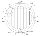
웨이퍼 제조의 특정 단계에서, 웨이퍼는 필름 프레임 상에 장착될 수 있다. 예를 들어, 웨이퍼가 절단(sawn)될 때, 일반적으로 필름 프레임 상에 장착된다. 절단 이후, 이러한 필름 프레임 상의 절단된(sawn) 웨이퍼는 외관적(cosmetic) 및/또는 다른 유형의 결함에 대하여 추가적으로 검사된다. 도 1a는 필름 프레임(30) 상에 장착된 웨이퍼(10)를 개략적으로 나타낸 것이고, 상기 필름 프레임은 상기 웨이퍼(10)를 얇은 물질의 층 또는 필름(32)에 의해 운반하며, 이는 일반적으로 상기 웨이퍼(10)가 장착되는 접착제 또는 점착성 면(tacky side)을 포함하고, 당업자에 의해 용이하게 이해되는 방법에 의한다. 상기 웨이퍼(10)는 여러 다이(die, 12)를 포함하고, 이는 생성되었거나, 제조 중에 분명해지는 수평 눈금선(6) 및 수직 눈금선(8)에 의해 서로 분리 또는 구획된다. 이러한 수평 및 수직 눈금선(6, 8)은 각각 상기 다이(die)의 수평 및 수직면(11, 16)에 대응되거나, 이를 구획한다. 당업자는 웨이퍼(10)가 웨이퍼 정렬 작업을 용이하게 하기 위하여, 일반적으로 적어도 하나의 기준 형상(reference feature, 11)을 포함하는 것을 이해할 것이고, 예를 들어, 이는 원형 주변부 이외의 노치(notch) 또는 직선부(straight portion) 또는 "평평한" 부분이다. 관련 기술 분야의 당업자는 또한, 상기 필름 프레임(30)이 필름 프레임의 정렬 작업을 용이하게 하기 위하여, 여러 등록 또는 정렬 형상(34a-b)을 포함하는 것을 이해할 것이다. 상기 필름 프레임(30)은 또한, "플랫(flat)"(35a-b)과 같은 다른 여러 기준 형상을 포함할 수 있다.
In certain stages of wafer fabrication, the wafer may be mounted on a film frame. For example, when the wafer is sawn, it is typically mounted on a film frame. After cutting, sawn wafers on these film frames are additionally inspected for cosmetic and / or other types of defects. 1a schematically depicts a
광학적 검사와 관련하여, 상기 웨이퍼(10) 상의 다이(12)는, 상기 다이(12) 상의 외관적(cosmetic) 또는 다른(예를 들어, 구조적인) 결함의 확인을 용이하게 하는 검사 기준에 따라서 자동적으로 검사 또는 시험된다. 상기 검사 기준을 만족하는 다이(12), 뿐만 아니라 상기 검사 기준을 만족하지 못하는 다이(12)도 각각 "통과(pass)" 또는 "실패(fail)"의 지정에 따라 추적하거나 카테고리화 할 수 있다. 모든 검사 기준을 성공적으로 만족하는 다이(12)는 추가적인 처리(processing) 또는 통합 회로 패키지에 도입하기에 적절한 반면, 모든 검사 기준을 만족하지 못하는 다이(12)는 (a) 폐기; (b) 실패 원인(들)의 분석 및 추후 실패의 방지; 또는 (c) 특정 상황에서 재가공/재처리될 수 있다.
In connection with the optical inspection, the
광학적 검사는 각각의 다이(12) 또는 다이(12)의 배열에 대한 화상(illumination)을 감독하고; 이미지 캡쳐 디바이스를 사용하여 상기 다이(12)로부터 반사되는 화상을 캡쳐하고 상기 다이(12)에 해당하는 이미지 데이터를 생성하며; 상기 이미지 데이터에 대한 이미지 처리 작업을 수행하여 하나 이상의 결함이 상기 다이(12)에 존재하는지 여부를 확인하는 것을 포함한다. 광학적 검사는 일반적으로 상기 웨이퍼(12)가 움직이는 동안 "온-더-플라이(on-the-fly)"로 수행되고, 이로써 상기 웨이퍼(12)에 의해 운반되는 상기 다이(12)가 이미지의 캡쳐 작업 중에 상기 이미지 캡쳐 디바이스에 대하여 지속적으로 이동한다.
The optical inspection may supervise the illumination of the array of each die 12 or die 12; Capture an image reflected from the die (12) using an image capture device and generate image data corresponding to the die (12); And performing an image processing operation on the image data to ascertain whether one or more defects are present on the
웨이퍼(10) 전체의 검사는 상기 웨이퍼(10) 상의 각각의 다이(12)에 해당하는 검사 결과(예를 들어, 통과/실패 결과)의 산출을 요구한다. 주어진 임의의 다이(12)에 해당하는 검사 결과가 산출될 수 있기 전에, 상기 다이(12)의 전체 표면 영역은 우선 완전히 캡쳐되어야 한다. 다시 말해, 주어진 임의의 다이(12)의 완전한 검사는, 우선 상기 다이의 전체 표면 영역이 상기 이미지 캡쳐 디바이스에 의해 캡쳐되는 것을 요구하고, 각각의 상기 다이(12)의 전체적인 표면 영역에 해당하는 이미지 데이터가 산출 및 처리되어야 한다. 만약 상기 다이의 전체 표면 영역에 대한 이미지 데이터가 산출되지 않았다면, 상기 다이(12)에 대한 이미지 처리 작업은 완료될 수 없고, 검사 결과는, 상기 다이(12)의 전체 표면 영역 또는 "전체-다이 이미지"를 포괄하는 이미지 세트의 캡쳐가 생성될 때까지 산출될 수 없다. 그러므로, 만약 상기 다이(12)의 전체 표면 영역에 해당하는 이미지 데이터, 또는 전체-다이 이미지 데이터가 산출되지 않았다면, 상기 다이(12)에 대한 검사 결과의 산출은 불필요하게 연기되고, 이는 검사 공정의 처리율에 악영향을 미친다.
Inspection of the
이미지 처리를 위하여 다이의 전체 이미지를 완전하게 캡쳐하기 위해 요구되는 이미지 캡쳐 작업의 수가 더 클수록, 검사 처리율은 더 낮아진다. 이는 검사 공정의 처리율을 최대로 하기 위해서는, 모든 다이의 전체 표면 영역이 가능한 한 적게 캡쳐되는 것이 바람직하다.
The greater the number of image capture operations required to fully capture the entire image of the die for image processing, the lower the throughput of inspection. It is desirable that the entire surface area of all the die is captured as little as possible in order to maximize the throughput of the inspection process.
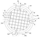
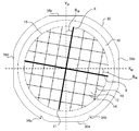
상기 웨이퍼(10)의 배향(orientation)의 오류는 필름 프레임(30) 상에 상기 웨이퍼(10)가 장착되는 중에 발생할 수 있다. 일반적으로, 웨이퍼 장착에 있어서의 오류는 필름 프레임 플랫(35a)과 같이, 주어진 필름 프레임 기준 형상에 대하여 웨이퍼 플랫 또는 노치(11)가 적절하게 배열되지 않는 것과 관련이 있다. 도 1b는 상기 웨이퍼(10)를 운반하는 필름 프레임(30)에 대하여 회전적으로 잘못 정렬된 웨이퍼(10)를 개략적으로 나타낸 것이다. 도 1b에 도시된 상기 웨이퍼(10)가 이의 필름 프레임(30)에 대해 나타내는 회전 배향이 도 1a에 도시된 웨이퍼(10)가 이의 필름 프레임(30)에 대해 나타내는 회전 배향과 명확하게 다른 것을 알 수 있다. 보다 구체적으로, 도 1b에서는 제1 필름 프레임 플랫(35a)에 대하여 각각 평행 또는 수직한 것으로 정의된 수평 기준축(36) 및/또는 수직축(38)에 대하여, 한 쌍의 수평 및 수직 웨이퍼 눈금선(6, 8)이 회전되어 있고, 도 1a에 도시된 웨이퍼(10)에 비하여 각도적인 단차(offset), 즉 각도 θ만큼 잘못 정렬되어 있는 것을 알 수 있다.
Errors in the orientation of the
다시 말해, 도 1a에 도시된 상기 웨이퍼(10)에 있어서, 제1 필름 프레임 플랫(35a)에 대하여 소정의 배향을 갖는 기준축(36, 38)으로부터, 웨이퍼 눈금선(6,8)이 회전된 각도의 크기를 나타내는 각도 θ는 약 0(zero)이다. 도 1b에 도시된 웨이퍼(10)에 있어서는, 상기 웨이퍼의 필름 프레임에 대한 정렬불량 각도 θ가 0(zero)이 아니다. 웨이퍼의 크기가 커짐에 따라, 구체적으로 보다 큰 웨이퍼 크기(예를 들어, 12 인치 또는 그 이상)에 대해서는, 상기 필름 프레임(30)에 대면하여(vis-a-vis) 장착된 웨이퍼(10)의 회전 정렬불량이, 일반적으로 그 상부에 장착된 웨이퍼의 검사 중에 문제를 야기하며, 이하 추가적으로 상세히 설명한다.
In other words, in the
주어진 다이(12)의 이미지 캡쳐 중에, 검사 시스템의 이미지 캡쳐 디바이스는 오직 상기 이미지 캡쳐 디바이스의 시야(FOV, field of view) 내에 위치하는 다이의 표면 영역 부분으로부터 반사된 화상(illumination)만 캡쳐할 수 있다. 상기 이미지 캡쳐 디바이스의 시야(FOV)에서 벗어난 상기 다이의 표면 영역 부분은 상기 이미지의 일부로 캡쳐될 수 없고, 또 다른 이미지의 일부로 캡쳐되어야 한다. 전술한 바와 같이, 검사 공정 처리율의 최대화는 상기 웨이퍼(10) 상의 모든 다이(12)의 표면 전체 영역이 가능한 한 적게 캡쳐되는 것을 요구한다. 다수의 이미지 캡쳐 작업이 다이의 전체 표면 영역에 해당하는 이미지 데이터를 산출하기 위해 요구되는 경우, 상기 다이(12)에 대한 검사 결과의 생성은 지연되며, 처리율에 악영향을 미친다. 상기 웨이퍼(10) 상의 각각의 다이(12)는 그러므로, 상기 웨이퍼 상의 모든 다이(12)에 대한 전체-다이 이미지(entire-die image) 데이터를 생성하기 위해 요구되는 이미지 캡쳐 작업의 수를 최소화하기 위하여 상기 이미지 캡쳐 디바이스 시야(FOV)에 대해 적절하게 정렬되어야 하고, 이로써 검사 공정 처리율이 최대화된다.
During image capture of a given
상기 다이(12)의 상기 이미지 캡쳐 디바이스 시야(FOV)에 대한 적절한 정렬은, 상기 이미지 캡쳐 디바이스 시야에 대한 상기 다이(12)의 어떠한 회전적 또는 각도적 정렬불량이 충분히 작거나, 최소이거나, 무시할 수 있고, 상기 다이의 전체 표면 영역이 상기 시야(FOV) 내에 위치하게 되는 상황으로 정의될 수 있다. 도 2a는 이미지 캡쳐 디바이스 시야(FOV)(50)에 대하여 적절하게 위치된 또는 정렬된 다이(12)를 개략적으로 나타낸 것이다. 도 2a에 명확하게 나타난 바와 같이, 상기 시야(50)에 대해 다이가 적절하게 정렬되면, 상기 다이(12)의 수평 경계(horizontal border) 또는 측면(14)이 실질적으로 시야(FOV)의 수평축(XI)에 평행하게 정렬되고, 수직 경계(vertical border) 또는 측면(16)이 시야(FOV)의 수직축(YI)에 평행하게 정렬된다. 결과적으로, 이러한 다이(12)의 전체 표면 영역은 상기 시야(50) 내에 위치하고, 상기 다이(12)의 전체 표면 영역은 한 번의 이미지 캡쳐 작업(event, operation) 또는 "스냅(snap)"에 의해 캡쳐될 수 있다.
Proper alignment of the die 12 with respect to the image capture device field of view (FOV) may be achieved by any rotational or angular misalignment of the die 12 with respect to the image capture device field of view being sufficiently small, And the entire surface area of the die is located within the field of view (FOV). 2A schematically illustrates a die 12 that is properly positioned or aligned with respect to an image capture device field of view (FOV) 2a, when the die is properly aligned with respect to the field of
도 2b는 이미지 캡쳐 디바이스 시야(50)에 대하여 적절하지 못하게 위치된 또는 잘못 정렬된 다이(12)를 개략적으로 나타낸 것이다. 도 2b는 상기 다이의 수직 및 수평 측면(14, 16)이, 상기 시야(FOV)의 수평축(XI) 및 상기 시야(FOV)의 수직축(YI) 각각에 대하여 회전되거나, 각도적으로 단차(offset)를 갖고, 상기 다이의 표면 영역 일부가 상기 시야(50)를 벗어나 위치하는 것을 명확하게 나타낸다. 상기 다이(12)의 상기 시야(50)에 대한 이러한 정렬불량 때문에, 상기 다이(12)의 전체 표면 영역에 해당하는 이미지 데이터의 산출이, 상기 다이(12)의 서로 다른 부분을 캡쳐하는 여러 이미지 캡쳐를 요구하고, 검사 공정 처리율을 감소시키게 된다. 보다 구체적으로는, 도 2c에 나타난 바와 같이, 이러한 회전적으로 잘못 정렬된 다이(12)의 전체 표면 영역을 캡쳐하기 위해 최대 4개의 이미지가 요구되며, 이는 상기 시야(FOV)에 대한 상기 다이의 정렬불량의 정도에 의존한다.
FIG. 2B schematically illustrates a die 12 that is improperly positioned or misaligned relative to the image capture device field of
필름 프레임이 조작되는 경우, 일반적으로는 기기적 필름 프레임 등록 절차가 이루어져야 한다. 보통, 상기 필름 프레임 등록 절차는 상기 필름 프레임이 상기 웨이퍼 테이블 상에 위치할 때 수행된다. 일부 시스템에서는, 2011년 5월 12일에 출원된 "웨이퍼 및 필름 프레임과 같은 구성 요소 구획을 조작 및 정렬하기 위한 시스템 및 방법(System and Method for Handling and Aligning Component Panes such as Wafers and Film Frames)"을 발명의 명칭으로 한 싱가포르 특허 출원번호 201103524-3에 기재된 바와 같이, 기계적인 필름 프레임 등록은 상기 웨이퍼 테이블 상에 상기 필름 프레임을 위치시키기 전에 이루어질 수 있고, 예를 들어, 상기 웨이퍼 테이블 상에 상기 필름 프레임을 위치시키기 전에, 상기 필름 프레임을 운반하는 단부 작동기(end effector)가 필름 프레임 정렬 형상(34a-b)을 필름 프레임 등록 요소 또는 구조와 결합시키는 때에 이루어질 수 있다.
When a film frame is manipulated, a mechanical film frame registration procedure should generally be performed. Usually, the film frame registration procedure is performed when the film frame is positioned on the wafer table. In some systems, the "System and Method for Handling and Aligning Component Panes such as Wafers and Film Frames " filed on May 12, 2011, A mechanical film frame registration may be made prior to placing the film frame on the wafer table as described in Singapore Patent Application No. 201103524-3, entitled " An end effector that carries the film frame may be brought into contact with the film frame alignment feature (34a-b) prior to positioning the film frame with the film frame registration element or structure.
기기적인 필름 프레임 등록 절차는 일정량의 조작 시간을 수반한다. 그러나, 상기 필름 프레임 등록 절차는 일반적으로, 상기 필름 프레임(30)이 상기 이미지 캡쳐 디바이스 시야(FOV)에 대해 적절하게 정렬 또는 등록되는 것을 보장한다. 그러나, 이는 상기 웨이퍼가 상기 필름 프레임 상의 첫 번째 위치에 적절하게 장착되되, 항상 그러한 것은 아님을 가정한다. 상기 필름 프레임 상에 장착된 상기 웨이퍼가 회전 정렬불량을 갖는 경우, 이는 검사에 문제 또는 지연을 일으키며, 하기 상세히 기재된 바와 같이 처리율에 악영향을 미친다.
The mechanical film frame registration procedure involves a certain amount of manipulation time. However, the film frame registration procedure generally ensures that the
상기 필름 프레임 등록 절차는 필름 프레임 등록 형상(34a-b)과 하나 이상의 필름 프레임 등록 구성을 맞대어 결합하는 방법으로 수행되며, 이는 통상적으로 웨이퍼 테이블 어셈블리에 의해 수행된다. 필름 프레임(30)이 등록된 이후에, 상기 필름 프레임(30)에 장착된 상기 웨이퍼(10) 상의 다이(12)는 상기 이미지 캡쳐 디바이스 시야(FOV)에 대하여 적절하게 정렬될 것으로 예상된다. 그러나, 만약, 상기 필름 프레임(30)에 장착된 상기 웨이퍼(10)에 약간의 또는 최소한의 양보다 많은 회전적 또는 각도적 배향 불량이 존재하는 경우, 상기 다이(12)는 상기 이미지 캡쳐 디바이스 시야(FOV)에 대해 적절하게 정렬되지 않을 것이다. 그러므로, 필름 프레임(30) 상에 상기 웨이퍼(10)가 장착되는 중에 발생하는 웨이퍼(10)의 어떤 회전 정렬불량의 정도가 상기 웨이퍼(12) 상의 각각의 다이(12)의 전체 표면 영역을 캡쳐하기 위해 요구되는 이미지의 수에 악영향을 미칠 수 있고, 결국 상기 웨이퍼(10)의 상기 필름 프레임(30)에 대한 어떤 회전 정렬불량의 정도가 검사 처리율에 악영향을 미칠 수 있음은 당연한 것이다.
The film frame registration procedure is performed in such a way that the film frame registration features 34a-b and at least one film frame registration configuration are mated together, which is typically performed by a wafer table assembly. After the
상기 웨이퍼(10)의 상기 필름 프레임(30)에 대한 적절한 정렬은 상기 이미지 캡쳐 디바이스 시야(50)에 대한 상기 다이(12)의 적절한 정렬을 보장한다. 상기 웨이퍼(10)가 이의 필름 프레임(30)에 대하여 적절하게 정렬하는 것은 하나 이상의 웨이퍼 눈금선(6,8)이, 필름 프레임 플랫(35a-d) 및/또는 상기 이미지 캡쳐 디바이스 시야(FOV)와 같은 하나 이상의 필름 프레임의 구조적 형상에 대하여 소정의 표준 정렬을 갖고, 이로써 상기 각각의 다이(12)가 상기 이미지 캡쳐 디바이스 시야(FOV)에 대하여, 도 2a에 나타난 방식으로 위치되는 상황 (즉, 상기 시야(FOV)의 수평 및 수직축(XI 및 YI) 및 각각의 다이의 수평 및 수직 측면(14, 16))으로 정의될 수 있다. 상기 웨이퍼(10)의 상기 필름 프레임(30)에 대한 이러한 정렬은 각각의 다이의 전체 표면 영역을 캡쳐하기 위해 요구되는 이미지 캡쳐 작업의 수를 최소화하며, 이로써 검사 공정 처리율을 최대화게 된다.
Proper alignment of the
추가적으로 설명하기 위하여, 도 2d가 상기 필름 프레임(30)에 대하여 적절하게 장착되고 정렬된 웨이퍼(10)와 검사 공정 웨이퍼 이동 경로(inspection process wafer travel path)를 개략적으로 나타내며, 이미지 캡쳐 디바이스는 상기 검사 공정 웨이퍼 이동 경로를 따라서 상기 웨이퍼(10) 상의 다이(12)의 연속적인 행(row) 내의 각각의 다이(12)의 전체 표면 영역의 이미지를 캡쳐한다. 도 2d에는 대표적인 2개의 다이(die) 행(row)이 지정되어 있고, 행 "A"의 다이(12) 및 행 "B"의 다이로 지칭한다. 상기 웨이퍼(10)는 이의 필름 프레임(30)에 대하여 적절하게 정렬되었기 때문에, 검사 공정 중에, 행 "A" 내의 각각의 다이(12)의 전체 표면 영역이 (예를 들어, 상기 웨이퍼(10)가 이동하는 동안, 즉 "온-더-플라이(on-the-fly)"로 이동하는 동안) 한 번의 해당 이미지로 캡쳐될 수 있다. 상기 행 "A"의 다이에 해당하는 이미지가 캡쳐된 이후에, 상기 웨이퍼(10)는 즉시, 최근 처리된 행 "A"의 다이(12)에 근접한 행 "B"의 다이(12)의 표면 영역이 상기 이미지 캡쳐 디바이스에 의해 캡쳐되도록 배치되고, 반대 방향으로 이동하면서 검사가 지속된다. 즉, 상기 검사 이동 경로는 "구불구불(serpentine)"하다. 상기 웨이퍼(10)가 상기 필름 프레임(30)에 대하여 적절하게 정렬되어 있기 때문에, 한번 더 반복하는 경우, 상기 검사 공정 중에, 행 "B" 내의 각각의 다이(12)의 전체 표면 영역은 한 번의 해당 이미지로 캡쳐될 수 있다. 상기 웨이퍼(10)가 이의 필름 프레임(30)에 대해 적절히 정렬된 경우, 이러한 방식으로 상기 웨이퍼(10) 전체를 검사함으로써 검사 공정 처리율의 최대치를 얻게 된다.
2d schematically shows the
도 2e는 상기 웨이퍼를 운반하는 필름 프레임(30)에 대하여 회전적으로 잘못 정렬된 웨이퍼(10)를 개략적으로 도시한 것이고, 임의의 한 번의 이미지 캡쳐 작업(event) 중에 이미지 캡쳐 디바이스가 캡쳐하면서 지나게 되는 검사 공정 웨이퍼 이동 경로는, 상기 웨이퍼(10) 상의 다이(12)의 연속적인 행(row) 내에 있는 각각의 다이(12)의 전체 표면 영역보다 더 적다. 광학적 검사 공정 중에, 이러한 웨이퍼의 필름 프레임에 대한 회전 정렬불량에 기인하여, 상기 웨이퍼(10)에 의해 운반되는 상기 다이(12)의 수평 및 수직 측면(14, 16)이, 각각 상기 시야(FOV)의 수평 및 수직축(XI 및 YI)으로부터, 회전적으로 단차(offset)를 갖게 될 것이며, 심지어 상기 필름 프레임(30)이 그 자체로 상기 이미지 캡쳐 디바이스에 대해 적절하게 등록된 때에도 그러할 것이다. 결과적으로, 주어진 다이(12)의 전체 표면 영역은 상기 이미지 캡쳐 디바이스 시야(50) 내에 놓일 수 없고, 개별적인 여러 이미지가 주어진 다이의 전체 표면 영역을 캡쳐하기 위해 요구될 것이다. 여러 이미지가 상기 다이의 전체 표면 영역을 캡쳐한 이후까지 상기 다이(12)에 대한 검사 결과가 산출될 수 없기 때문에, 상기 다이(12)에 해당하는 검사 결과의 산출은 바람직하지 않게 지연된다.
Figure 2e is a schematic illustration of a
전술한 바와 같은 유사한 고려 사항이, 다이(12)의 그룹(group)에 관한 검사 시에도 적용된다. 도 2f는 다이의 배열(18)을 개략적으로 도시한 것이고, 여기서 상기 다이의 배열(18) 내에 모든 다이(12)의 총 표면 영역이 이미지 캡쳐 디바이스 시야(50)보다 더 작으며, 이는 상기 다이의 배열(18) 내에 있는 각각의 다이(12)의 수평 및 수직 측면(14, 16)이 상기 시야(FOV)의 수평축(XI) 및 상기 시야의 수직축(YI) 각각에 대하여 실질적으로 평행하기 때문에 상기 다이의 배열(18)이 상기 이미지 캡쳐 디바이스 시야(50)에 대하여 적절하게 정렬된 것이다. 결과적으로, 상기 다이의 배열(18)은 모두 상기 이미지 캡쳐 디바이스에 의해 단일의 이미지로 캡쳐될 수 있고, 이로써 검사 공정 처리율은 최대화된다. 도 2g는 상기 다이의 배열(18) 내에 있는 상기 다이(12)의 수평 및 수직 측면(14, 16)이 상기 시야(FOV)의 수평 및 수직축(XI 및 YI)에 대하여 적절하게 정렬되지 않은 다이의 배열(18)을 개략적으로 도시한 것이다. 즉, 상기 다이의 배열(18)의 일부는 상기 시야(5)를 벗어나 위치한다. 결과적으로, 상기 다이의 배열(18)은 이에 대해 검사 결과가 산출되기 이전에, 여러 이미지가 캡쳐되어야 하고, 이로써 처리율을 저하시키게 된다.
Similar considerations, such as those discussed above, also apply to the inspection of the group of dies 12. 2f schematically shows an
더욱이, 전술한 바와 유사한 고려 사항이, 단일의(예를 들어, 큰) 다이(12)가 상기 시야(50)보다 더 큰 표면 영역을 갖고, 상기 이미지 캡쳐 디바이스 시야(50)에 대해 적절하게 배열된 경우의 검사 시에도 적용된다. 도 2h는 이미지 캡쳐 디바이스의 시야(50)보다 더 큰 표면 영역을 갖는 다이(12)를 개략적으로 도시한 것이다. 이러한 다이(12)는 또한, 상기 다이의 수평 및 수직 측면(14, 16)이 상기 시야(FOV)의 수평 및 수직축(XI 및 YI)에 대하여 실질적으로 평행함으로써, 상기 시야(5)에 대해 적절하게 배치되된다. 결과적으로, 상기 다이(12)의 전체 표면 영역은 최소의 이미지 캡쳐 작업으로 캡쳐될 수 있다. 이러한 예시에서, 상기 이미지 캡쳐 디바이스는 상기 다이(12)의 전체 표면 영역의 검사를 위한 이미지를 총 9개 캡쳐해야 하고, 이는 상기 다이의 전체 표면 영역의 서로 다른 부분들을 상기 이미지 캡쳐 디바이스에 대하여 연속적으로 위치시킴으로써 수행하며, 각각이 이러한 상대적 위치에 놓인 동안에, 상기 이미지 캡쳐 디바이스 시야(50) 내에 위치한 상기 다이의 표면 영역의 각 부분의 이미지를 캡쳐한다.
Furthermore, considerations similar to those described above may be applied to the case where a single (e.g., large) die 12 has a larger surface area than the field of
도 2i는 도 2h에 도시된 바와 같은 하나의 다이(12)를 개략적으로 도시한 것이고, 이는 시야(FOV)에 대하여 적절하게 정렬된 조건 하에서는 9개의 이미지를 캡쳐함으로써 완전히 검사될 수 있으나, 다이의 수평 및 수직 측면이 상기 시야(FOV)의 수평 및 수직축(XI 및 YI)에 대하여 잘못 정렬된 경우에는 다이(12)의 일부가 9개의 이미지가 캡쳐된 이후임에도, 상기 이미지 캡쳐 디바이스 시야(50)를 벗어나 놓이게 된다.
Figure 2i schematically depicts one die 12 as shown in Figure 2h which can be fully inspected by capturing nine images under properly aligned conditions for field of view FOV, If the horizontal and vertical sides are misaligned with respect to the horizontal and vertical axes X I and Y I of the field of view FOV then the image capture device field of view (even though nine of the images have been captured) 50).
종래의 시스템 및 방법은 웨이퍼(10)와 필름 프레임(30)의 회전 정렬불량을 교정 또는 수정하기 위하여, 수동적 개입(manual intervention) 또는 회전 가능한 웨이퍼 테이블(rotatable wafer table) 중 어느 하나에 의한다. 전술한 바와 같이, 수동적 개입은 시스템 처리율에 악영향을 미친다. 회전 가능한 웨이퍼 테이블과 관련하여, 이러한 웨이퍼 테이블은 웨이퍼-필름 프레임의 회전 정렬불량을 교정 또는 실질적으로 교정하기에 충분한 회전 변위량을 선택적으로 제공하도록 구성된다. 웨이퍼(10)와 필름 프레임(30)의 정렬불량의 크기는 양의 방향 또는 음의 방향으로 예를 들어, 10 ~ 15도 또는 그 이상의 상당한 크기의 도(degree)의 범위로 나타날 수 있다. 불행히도, 회전을 제공하도록 구성된 웨이퍼 테이블은 기기적인 관점에서 복잡하여 바람직하지 못하며, 상대적으로 고가(예를 들어, 상당히 고가)이다. 나아가, 이러한 회전적인 웨이퍼 테이블의 변위를 제공하는 웨이퍼 테이블 어셈블리의 추가적인 구조적 복잡성은, 검사 중에, 상기 웨이퍼 테이블 표면을 상기 이미지 캡쳐 디바이스의 광학축(optical axis)에 수직한 단일 평면으로 균일하게 유지하는 것을 더욱 어렵게 한다.
Conventional systems and methods are either manual intervention or rotatable wafer tables to calibrate or correct defective rotational alignment of the
웨이퍼 및 필름 프레임을 모두 조작하기 위한 단일 웨이퍼 테이블 구조를 제공하는 웨이퍼 및 필름 프레임 조작 시스템에 대한 필요성이 존재하며, 이는 웨이퍼의 휨(warpage), 예측 불가능한 횡방향의 웨이퍼 이동, 및 웨이퍼-필름 프레임 회전 정렬불량으로부터 야기되는 전술한 문제점들 중 적어도 일부를 자동 극복할 수 있고, 검사 공정 처리율을 최대화하거나 향상시킬 수 있다.
There is a need for a wafer and film frame manipulation system that provides a single wafer table structure for manipulating both the wafer and the film frame, including warpage of the wafer, unpredictable lateral wafer movement, It is possible to automatically overcome at least some of the above-mentioned problems arising from rotational misalignment and to maximize or improve the inspection process throughput.
웨이퍼 및 필름 프레임을 모두 조작하기 위한 단일 웨이퍼 테이블 구조를 제공하는 웨이퍼 및 필름 프레임 조작 시스템에 대한 필요성이 존재하며, 이는 웨이퍼의 휨(warpage), 예측 불가능한 횡방향의 웨이퍼 이동, 및 웨이퍼-필름 프레임 회전 정렬불량으로부터 야기되는 전술한 문제점들 중 적어도 일부를 자동 극복할 수 있고, 검사 공정 처리율을 최대화하거나 향상시킬 수 있다.
There is a need for a wafer and film frame manipulation system that provides a single wafer table structure for manipulating both the wafer and the film frame, including warpage of the wafer, unpredictable lateral wafer movement, It is possible to automatically overcome at least some of the above-mentioned problems arising from rotational misalignment and to maximize or improve the inspection process throughput.
본 발명의 태양에 따르면, 필름 프레임 상부에 장착된 웨이퍼의 회전 정렬불량을 수정하기 위한 시스템이 필름 프레임을 그 상부에 안정적으로 유지하도록 구성된 웨이퍼 테이블 표면을 제공하는 웨이퍼 테이블; 필름 프레임 상부에 장착되고 상기 웨이퍼 테이블 표면에 의해 유지되는 웨이퍼에 대한 검사 절차를 수행하도록 구성된 제1 이미지 캡쳐 디바이스를 구비한 웨이퍼 검사 시스템; 상기 필름 프레임 상부에 장착된 상기 웨이퍼의 부분 중 적어도 하나의 이미지를 캡쳐하도록 구성된 제2 이미지 캡쳐 디바이스; 및 상부에 상기 웨이퍼가 장착된 상기 필름 프레임을 상기 웨이퍼 테이블 표면으로 이송하고, 상기 필름 프레임, 상기 제1 이미지 캡쳐 디바이스, 및/또는 상기 제2 이미지 캡쳐 디바이스에 대한 상기 웨이퍼의 임의의 회전 정렬불량을 수정하기 위해 상기 필름 프레임을 회전시키도록 구성된 필름 프레임 조작 장치를 포함한다. 상기 웨이퍼 검사 시스템은 필름 프레임 정렬 형상을 등록 구성의 세트와 맞대어 결합함으로써 확인하는 단계를 포함하는 필름 프레임 등록 절차에 대한 필요성 없이 상기 검사 절차를 시작하도록 구성될 수 있다.
According to an aspect of the present invention there is provided a system for correcting rotational misalignment of a wafer mounted on a film frame, the wafer table providing a wafer table surface configured to stably hold the film frame thereon; A wafer inspection system having a first image capture device configured to perform an inspection procedure on a wafer mounted on a film frame and held by the wafer table surface; A second image capture device configured to capture an image of at least one of the portions of the wafer mounted on top of the film frame; And transferring the film frame, on which the wafer is mounted, to the wafer table surface, and transferring the film to the wafer table surface with an arbitrary rotational misalignment of the wafer relative to the film frame, the first image capture device, and / And a film frame manipulation device configured to rotate the film frame to modify the film frame. The wafer inspection system can be configured to start the inspection procedure without the need for a film frame registration procedure comprising confirming by binding the film frame alignment feature against a set of registration configurations.
상기 제1 이미지 캡쳐 디바이스는 상기 제2 이미지 캡쳐 디바이스와 동일한 것이거나, 별개인 것일 수 있다. 예를 들어, 상기 제2 이미지 캡쳐 디바이스는 상기 웨이퍼 검사 시스템과 별개일 수 있으며, 상기 제2 이미지 캡쳐 디바이스는 상기 필름 프레임이 상기 웨이퍼 테이블 표면 상에 위치하기 전에, 예를 들어 상기 필름 프레임이 이동하는 동안에, 상기 필름 프레임 상부의 상기 웨이퍼 부분의 적어도 하나의 이미지를 캡쳐하도록 구성될 수 있다.
The first image capture device may be the same as or different from the second image capture device. For example, the second image capture device may be separate from the wafer inspection system, and the second image capture device may be configured to move the film frame before the film frame is positioned on the wafer table surface, The apparatus may be configured to capture at least one image of the portion of the wafer above the film frame.
상기 시스템은 상기 필름 프레임 상부에 장착된 상기 웨이퍼 부분의 적어도 하나의 이미지를 분석하여, 상기 적어도 하나의 이미지에 대한 이미지 처리 작업을 수행하는 프로그램 명령의 실행에 의해, 상기 웨이퍼의 상기 필름 프레임 또는 상기 제1 이미지 캡쳐 디바이스 혹은 상기 제2 이미지 캡쳐 디바이스의 시야에 대한 회전 정렬불량 각도 및 회전 정렬불량 방향을 확인하기 위해 구성된 처리 유닛을 더 포함한다. 상기 이미지 처리 작업은 웨이퍼 플랫 및 웨이퍼 눈금선 세트 중 적어도 하나를 포함하는 하나 이상의 웨이퍼 구조 및/또는 시각적 형상; 및 가능하게는 필름 프레임 플랫을 포함하는 하나 이상의 필름 프레임 구조 및/또는 시각적 형상을 확인하도록 구성된다.
Wherein the system is configured to analyze at least one image of the portion of the wafer mounted on top of the film frame and to execute the image processing operation on the at least one image, Further comprising a processing unit configured to identify a rotational alignment defective angle and a rotational alignment defective direction for the field of view of the first image capture device or the second image capture device. Wherein the image processing operation comprises one or more wafer structures and / or visual features comprising at least one of a wafer flat and a set of wafer scale lines; And possibly one or more film frame structures and / or visual features including film frame flats.
상기 필름 프레임 조작 장치는 상기 필름 프레임을 상기 정렬불량 방향과 반대 방향으로, 상기 회전 정렬불량 각도에 대응되는 각도 크기만큼 회전시키도록 구성된다. 상기 웨이퍼의 회전 정렬불량의 수정은 필름 프레임 조작 처리율 또는 검사 공정의 처리율을 저하시키지 않으면서 수행되고, 예를 들어, 상기 필름 프레임이 상기 필름 프레임 조작 장치에 의해 상기 웨이퍼 테이블 표면 상에 위치하기 전, 이동 중에 수행된다.
The film frame manipulation device is configured to rotate the film frame in a direction opposite to the misalignment direction by an angle magnitude corresponding to the misalignment angle of the misalignment. The correction of the rotational misalignment of the wafer is carried out without degrading the film frame handling rate or the throughput of the inspection process. For example, before the film frame is positioned on the wafer table surface by the film frame handling device , And on the move.
상기 필름 프레임 조작 장치는 본체; 상기 본체에 결합되고 부압에 의해 상기 필름 프레임의 경계 부분에 결합되도록 구성된 복수의 진공 구성; 및 상기 복수의 진공 구성과 상기 필름 프레임 경계를 용이하게 결합시키기 위한 각각의 별개 위치게 상기 복수의 진공 구성을 위치시키기 위해 구성된 캡쳐 위치화 어셈블리를 포함하며, 상기 복수의 진공 구성은 상기 필름 프레임의 중심에 해당하는 공통축(common axis)에 다가가거나 멀어지도록 횡방향의 여러 별개의 위치로 제어 가능하게 이동할 수 있으며, 상기 각각의 별개의 위치는 서로 다른 필름 프레임 크기에 대응된다.
The film frame manipulating apparatus comprises: a main body; A plurality of vacuum configurations coupled to the body and configured to be coupled to a boundary portion of the film frame by a negative pressure; And a capture locating assembly configured to position the plurality of vacuum configurations at respective discrete locations for easily coupling the plurality of vacuum configurations with the film frame boundary, And can controllably move to a plurality of different positions in the transverse direction to approach or move away from a common axis corresponding to the center, wherein each of the discrete positions corresponds to a different film frame size.
상기 필름 프레임 조작 장치는 또한, 상기 본체에 결합되고, 상기 복수의 진공 구성을 운반하는 이동 가능한 복수의 캡쳐 암(capture arm); 상기 필름 프레임에 대한 상기 웨이퍼의 회전 정렬불량에 대한 정확한 수정을 용이하게 하기 위하여, 상기 공통축에 대한 공통의 방향으로 상기 복수의 캡쳐 암을 선택적으로 및 동시에 회전시키도록 구성된 회전 정렬불량 보정 모터(rotational misalignment compensation motor); 및 상기 복수의 캡쳐 암을 웨이퍼 테이블 표면에 수직한(normal) 수직 방향을 따라 제어 가능하게 이동시키도록 구성된 수직 변위 구동기(vertical displacement driver)를 포함한다. 다양한 구현예에서, 상기 필름 프레임 조작 장치는 상기 필름 프레임을 상기 웨이퍼 테이블 상에 직접 위치시키도록 구성된다.
The film frame manipulation apparatus further includes a plurality of movable capture arms coupled to the body and carrying the plurality of vacuum configurations; A rotational alignment failure correction motor (12) configured to selectively and simultaneously rotate the plurality of capture arms in a common direction with respect to the common axis to facilitate correct correction of rotational alignment defects of the wafer relative to the film frame rotational misalignment compensation motor); And a vertical displacement driver configured to controllably move the plurality of capture arms along a normal vertical direction to the wafer table surface. In various embodiments, the film frame manipulation device is configured to position the film frame directly on the wafer table.
본 발명의 일 태양에 따르면, 필름 프레임 상부에 장착된 웨이퍼의 회전 정렬불량을 수정하는 공정은, 웨이퍼 검사 시스템 (예를 들어, 광학 검사 시스템)에 의해 상기 웨이퍼의 검사 절차를 시작하기 전에 이미지 캡쳐 디바이스를 이용하여 필름 프레임 상부에 장착된 웨이퍼의 적어도 하나의 이미지를 캡쳐하는 단계; 상기 웨이퍼의 상기 필름 프레임 및/또는 상기 이미지 캡쳐 디바이스의 시야의 기준축 세트에 대한 회전 정렬불량 각도 및 회전 정렬불량 방향을 확인하기 위해 상기 적어도 하나의 이미지를 이미지 처리 작업에 의해 디지털 방식으로 분석하는 단계; 상기 검사 시스템과 별개인 필름 프레임 조작 장치에 의해 상기 필름 프레임 및/또는 상기 이미지 캡쳐 디바이스의 시야의 기준축에 대한 상기 웨이퍼의 회전 정렬불량을 수정하는 단계를 포함한다.
According to one aspect of the present invention, the process of correcting the rotational misalignment of the wafer mounted on the top of the film frame is performed by a wafer inspection system (e.g., an optical inspection system) Capturing at least one image of the wafer mounted on top of the film frame using the device; The at least one image is digitally analyzed by an image processing operation to identify a rotational alignment defective angle and a rotational alignment defective direction for the film frame of the wafer and / or the reference axis set of fields of view of the image capture device step; And modifying the rotational misalignment of the wafer relative to the reference axis of the field of view of the film frame and / or the image capture device by a film frame manipulation device that is separate from the inspection system.
상기 적어도 하나의 이미지를 캡쳐하고 분석하며, 이러한 분석에 기초하여 상기 웨이퍼의 회전 정렬불량이 수정되기 때문에, 필름 프레임의 구조적 형상의 세트가, 상기 필름 프레임의 구조적 형상의 세트와 맞대어 결합하도록 구성된 대응 등록 구성의 세트에 대해 정렬되는 필름 프레임 등록 절차가 상기 검사 공정의 개시 전에 배제될 수 있다.
A set of structural features of the film frame is adapted to be coupled to a set of structural features of the film frame to capture and analyze the at least one image and to correct the rotational misalignment of the wafer based on such analysis, A film frame registration procedure arranged for a set of registration configurations may be excluded prior to the commencement of the inspection process.
상기 공정은 또한, 상기 필름 프레임을 상기 검사 시스템에 해당하는 웨이퍼 테이블의 웨이퍼 테이블 표면에 이송하는 단계를 포함한다. 상기 필름 프레임의 상기 웨이퍼 테이블로의 이송은 상기 웨이퍼 테이블 표면 상에 상기 필름 프레임을 직접 위치시키는 것을 포함한다. 상기 웨이퍼의 적어도 하나의 이미지를 캡쳐하고 회전 정렬불량을 수정하는 단계는 상기 필름 프레임이 상기 웨이퍼 테이블 표면 상에 위치하기 전에 수행될 수 있다. 상기 적어도 하나의 이미지를 캡쳐하는 단계는 상기 필름 프레임이 이동하는 동안에 수행될 수 있다. 대안적으로, 상기 적어도 하나의 이미지를 캡쳐하는 단계는 상기 필름 프레임이 상기 웨이퍼 테이블 표면 상에 이송된 이후에 수행될 수 있다. 즉, 상기 적어도 하나의 이미지를 캡쳐하는 단계는 상기 검사 시스템의 일부로 형성되거나, 이와는 별개인 이미지 캡쳐 디바이스에 의해 수행될 수 있다.
The process also includes transferring the film frame to the wafer table surface of the wafer table corresponding to the inspection system. The transfer of the film frame to the wafer table includes direct positioning of the film frame on the wafer table surface. Capturing at least one image of the wafer and modifying rotational alignment defects may be performed before the film frame is positioned on the wafer table surface. The capturing of the at least one image may be performed while the film frame is moving. Alternatively, capturing the at least one image may be performed after the film frame is transferred onto the wafer table surface. That is, the step of capturing the at least one image may be performed by an image capture device that is formed as part of the inspection system or is separate from the inspection system.
상기 회전 정렬불량 각도 및 상기 회전 정렬불량 방향을 확인하는 단계는 상기 적어도 하나의 캡쳐된 이미지에 대하여, 하나 이상의 웨이퍼 구조 및/또는 시각적 형상의 (i) 하나 이상의 필름 프레임 구조 및/또는 시각적 형상, 또는 상기 필름 프레임 구조 및/또는 시각적 형상에 관한 공간적 방향에 대한 배향을 검출하거나, (ii) 상기 이미지 캡쳐 디바이스의 시야의 기준축 세트에 대한 배향을 검출하기 위한 이미지 처리 작업을 수행하는 단계를 포함한다. 상기 웨이퍼 구조 및/또는 시각적 형상은 적어도 하나의 웨이퍼 플랫(wafer flat) 및 웨이퍼 눈금선 세트를 포함할 수 있고; 상기 필름 프레임 구조 및/또는 시각적 형상은 필름 프레임 플랫(film frame flat)을 포함할 수 있다. Wherein identifying the rotational misalignment angle and the rotational misalignment direction comprises: (i) determining, for the at least one captured image, one or more film structures and / or visual features of one or more wafer structures and / Or an orientation in a spatial direction with respect to the film frame structure and / or visual shape, or (ii) performing an image processing operation to detect an orientation with respect to a set of reference axes of the field of view of the image capture device do. The wafer structure and / or visual features may include at least one wafer flat and a set of wafer scale lines; The film frame structure and / or visual features may include a film frame flat.
상기 웨이퍼의 회전 정렬불량을 수정하는 단계는 상기 필름 프레임을 상기 정렬불량 방향과 반대 방향으로, 상기 회전 정렬불량 각도에 대응되는 각도 크기만큼 회전하는 단계를 포함한다. 상기 회전 정렬불량의 수정은 상기 필름 프레임이 상기 웨이퍼 테이블 표면 상에 위치하기 전에 수행되기 때문에, 상기 웨이퍼의 회전 정렬불량을 수정하는 단계는 필름 프레임 조작 처리율 또는 검사 공정의 처리율을 저하시키지 않으면서 수행될 수 있다.
The step of correcting the rotational misalignment of the wafer includes rotating the film frame in an opposite direction to the misalignment direction by an angular magnitude corresponding to the rotational misalignment angle. Since the correction of the rotational misalignment is performed before the film frame is positioned on the wafer table surface, the step of correcting the rotational misalignment of the wafer is performed without degrading the film frame handling throughput or the throughput of the inspection process .
웨이퍼 및 필름 프레임을 모두 조작하기 위한 단일 웨이퍼 테이블 구조를 제공하는 웨이퍼 및 필름 프레임 조작 시스템에 대한 필요성이 존재하며, 이는 웨이퍼의 휨(warpage), 예측 불가능한 횡방향의 웨이퍼 이동, 및 웨이퍼-필름 프레임 회전 정렬불량으로부터 야기되는 전술한 문제점들 중 적어도 일부를 자동 극복할 수 있고, 검사 공정 처리율을 최대화하거나 향상시킬 수 있다.
There is a need for a wafer and film frame manipulation system that provides a single wafer table structure for manipulating both the wafer and the film frame, including warpage of the wafer, unpredictable lateral wafer movement, It is possible to automatically overcome at least some of the above-mentioned problems arising from rotational misalignment and to maximize or improve the inspection process throughput.
도 1a는 필름 프레임 상에 장착된 웨이퍼를 개략적으로 나타낸 것이고, 상기 필름 프레임은 상기 웨이퍼가 장착된 측의 접착제 또는 점착성 있는(tack) 면을 포함하는 얇은 물질의 층 또는 필름에 의해 이를 운반한다.
도 1b는 상기 웨이퍼를 운반하는 필름 프레임에 대하여 회전적으로 잘못 정렬된 웨이퍼를 개략적으로 나타낸 것이다.
도 2a는 이미지 캡쳐 디바이스의 시야(FOV)에 대하여 적절하게 위치되거나, 정렬된 다이(die)를 개략적으로 나타낸 것이다.
도 2b는 이미지 캡쳐 디바이스 시야(FOV)에 대하여 적절하지 않게 위치되거나, 잘못 정렬된 다이(die)를 개략적으로 나타낸 것이다.
도 2c는 상기 시야(FOV)에 대한 상기 다이(die)의 정렬불량의 정도에 따라, 도 2b에 도시된 바와 같은 회전적으로 잘못 정렬된 다이의 전체 표면 영역을 캡쳐하기 위해 최대 4개의 이미지가 요구됨을 개략적으로 나타낸 것이다.
도 2d는 필름 프레임에 대하여 적절하게 장착되거나 정렬된 웨이퍼와 검사 공정 웨이퍼 이동 경로(inspection process wafer travel path)를 개략적으로 나타낸 것이고, 이미지 캡쳐 디바이스는 상기 검사 공정 웨이퍼 이동 경로를 따라서 상기 웨이퍼 상의 다이(die)의 연속적인 행(row) 내에 있는 각각의 다이(die)의 전체 표면 영역의 이미지를 캡쳐한다.
도 2e는 필름 프레임에 대하여 회전적으로 잘못 정렬된 웨이퍼(10)와 검사 공정 웨이퍼 이동 경로를 개략적으로 나타낸 것이고, 이미지 캡쳐 디바이스는 상기 검사 공정 웨이퍼 이동 경로를 따라서 상기 웨이퍼 상의 다이(die)의 연속적인 행(row) 내에 있는 각각의 다이의 전체 표면 영역보다 적은 영역의 이미지를 캡쳐하게 된다.
도 2f는 다이의 배열(die array)을 개략적으로 나타낸 것이고, 여기서 상기 다이의 배열 내에 있는 모든 다이의 전체 표면 영역은 이미지 캡쳐 디바이스의 시야(FOV)보다 더 작으며, 상기 다이의 배열 내에 있는 각각의 다이의 수평 및 수직 측면이 시야(FOV)의 수평 및 수직축(XI 및 YI)에 대해 각각 실질적으로 평행하므로 상기 다이의 배열이 상기 FOV에 대해 적절하게 정렬된 것이다.
도 2g는 다이의 배열(die array)을 개략적으로 나타낸 것이고, 여기서 상기 다이의 배열 내에 있는 다이의 수평 및 수직 측면은 시야(FOV)의 수평 및 수직축(XI 및 YI)에 대해 적절하지 않게 정렬된 것이다.
도 2h는 이미지 캡쳐 디바이스의 시야(FOV)보다 큰 표면 영역을 갖는 단일 다이(die)를 개략적으로 나타낸 것이고, 여기서 상기 다이는 이의 수평 및 수직 측면이 시야(FOV)의 수평 및 수직축(XI 및 YI)에 대해 각각 실질적으로 평행하므로 상기 시야(FOV)에 대해 적절하게 정렬된 것이다.
도 2i는 도 2h에 도시된 바와 같은 단일 다이(die)를 개략적으로 나타낸 것이고, 여기서 다이의 측면이 시야(FOV)의 수평 및 수직축(XI 및 YI)에 대해 잘못 정렬되어 상기 다이의 일부가 상기 이미지 캡쳐 디바이스의 시야(FOV)를 벗어나 위치하게 된다.
도 3a는 웨이퍼 및/또는 필름 프레임 조작 시스템의 부분들을 개략적으로 나타낸 것이고, 이는 웨이퍼 및 필름 프레임을 모두 조작하기 위한 하나의 다공성 웨이퍼 테이블 구조를 제공하며, 또한 본 발명에 개시된 구현예에 따라 회전 정렬불량 보정(rotational misalignment correction), 비평면성 교정(non-planarity remediation), 및/또는 횡방향 변위의 방지(lateral displacement prevention)를 제공한다.
도 3b는 웨이퍼 및/또는 필름 프레임 조작 시스템의 부분들을 개략적으로 나타낸 것이고, 이는 웨이퍼 및 필름 프레임을 모두 조작하기 위한 하나의 다공성 웨이퍼 테이블 구조를 제공하며, 또한 본 발명에 개시된 구현예에 따라 회전 정렬불량 보정, 비평면성 교정, 및/또는 횡방향 변위의 방지를 제공한다.
도 4a는 본 발명의 일 구현예에 따른 웨이퍼 테이블 베이스 트레이(wafer table base tray)의 사시도이고, 이는 비다공성 물질, 예를 들어 세라믹 계열의 비다공성 물질을 포함한다.
도 4b는 도 4a의 베이스 트레이의 A-A' 선에 대한 사시 단면도이다.
도 5a는 몰드성(moldable), 성형성(formable), 정합성(conformable) 또는 유동성(flowable)의 다공성 물질, 예를 들어 세라믹 계열의 다공성 물질이 내부에 존재하는 도 4a의 베이스 트레이의 사시도를 나타낸 것이다.
도 5b는 몰드성(moldable), 성형성(formable), 정합성(conformable) 또는 유동성(flowable)의 세라믹계 다공성 물질을 운반하는 도 5a의 베이스 트레이의 B-B' 선에 대한 사시 단면도 있다.
도 5c는 도 5a 및 5b에 해당하는 경화된 다공성 세라믹 물질을 운반하는 베이스 트레이에 대응되는, 평면화 공정 이후의(post-planarization process) 진공 척(vacuum chuck) 구조의 단면도이다.
도 5d는 본 발명의 일 구현예에 따라 제조된 진공 척 구조의 단면도이고, 이는 도 5c에 대응되며, 평면성의 진공 척 표면 상에 웨이퍼 또는 필름 프레임을 운반한다.
도 5e는 본 발명의 일 구현예에 따른, 진공 척 구조 상에 배치된 제1 표준 직경(예를 들어, 8인치)을 갖는 대표적인 제1 웨이퍼의 사시도이다.
도 5f는 본 발명의 일 구현예에 따른, 진공 척 구조 상에 배치된 제2 표준 직경(예를 들어, 12인치)을 갖는 대표적인 제2 웨이퍼의 사시도이다.
도 5g는 본 발명의 일 구현예에 따른, 진공 척 구조 상에 배치된 제3 표준 직경(예를 들어, 16인치)을 갖는 대표적인 제3 웨이퍼의 사시도이다.
도 6a는 본 발명의 다른 구현예에 따른 세라믹 계열의 진공 척 구조의 사시도이고, 이는 방출핀 가이드(ejector pin guide) 구성의 세트를 포함한다.
도 6b는 도 6a의 상기 세라믹 계열의 진공 척 구조의 C-C'선에 대한 단면도이다.
도 7a는 도 4a 및 4b의 베이스 트레이의 사시도이고, 그 내부에 몰드성(moldable), 성형성(formable), 정합성(conformable) 또는 유동성(flowable)의 세라믹계 다공성 물질이 배치되어 있다.
도 7b는 도 7a에 해당하는 몰드성(moldable), 성형성(formable), 정합성(conformable) 또는 유동성(flowable)의 세라믹계 다공성 물질을 운반하는 상기 베이스 트레이의 D-D'선에 대한 단면도이다.
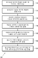
도 8은 본 발명의 일 구현예에 따른 진공 척 구조를 제조하는 대표적인 공정의 흐름도이다.
도 9는 본 발명의 일 구현예에 따른 진공 척 구조의 단면도이고, 이는 몰드성(moldable)의 세라믹계 다공성 물질의 초기 부피가 평면화 공정이 완료되기 전에 베이스 트레이의 구획부(compartment) 부피를 약간 초과하는 것을 나타낸다.
도 10a는 본 발명의 일 구현예에 따라 필름 프레임에 대한 웨이퍼의 회전적 또는 각도적 정렬불량의 정도를 확인하기 위해 구성된 정렬불량 검사 시스템(misalignment inspection system)의 구현예를 개략적으로 나타낸 것이다.
도 10b는 본 발명의 일 구현예에 따라 도 10a에 도시된 바와 같은 정렬불량 검사 시스템에 의하여 필름 프레임에 대한 웨이퍼의 회전적 또는 각도적 정렬불량의 정도를 확인하는 양상을 개략적으로 나타낸 것이다.
도 10c는 본 발명의 또 다른 구현예에 따라 필름 프레임에 대한 웨이퍼의 회전적 또는 각도적 정렬불량의 정도를 확인하기 위해 구성된 정렬불량 검사 시스템(misalignment inspection system)의 구현예를 개략적으로 나타낸 것이다.
도 10d는 본 발명의 일 구현예에 따라 상기 도 10c에 도시된 바와 같은 정렬불량 검사 시스템에 의하여 필름 프레임에 대한 웨이퍼의 회전적 또는 각도적 정렬불량의 정도를 확인하는 태양을 개략적으로 나타낸 것이다.
도 11은 제1 조작 하위시스템(first handling subsystem)의 등록 구성을 운반하는 적어도 하나의 단부 작동기(end effector)를 포함하는 단부 작동기의 세트를 개략적으로 나타낸 것이다.
도 12a는 본 발명의 일 구현예에 따라 웨이퍼 및 필름 프레임의 조작을 수행하기 위하여, 회전 보정 장치(rotation compensation apparatus), 평탄화 장치(flattening apparatus) 및 제한 장치(confinement apparatus) 각각이 결합(combined), 통합(integrated), 또는 통일(unified)된 방식으로 구성된 대표적인 다기능 조작 장치(multifunction handling apparatus)의 태양을 개략적으로 나타낸 것이다.
도 12b는 본 발명의 일 구현예에 따른 캡쳐 암(capture arm) 부분을 개략적으로 나타낸 것이다.
도 12c는 본 발명의 일 구현예에 따른 캡쳐 위치 어셈블리(capture positioning assembly)의 부분을 개략적으로 나타낸 것이고, 이는 제1 필름 프레임의 직경 또는 단면 영역에 대응되는 제1 위치에 복수의 캡쳐 암을 위치시키는 대표적인 제1 위치화(first positioning)를 나타낸 것이다.
도 12d는 캡쳐 위치 어셈블리(capture positioning assembly)의 부분을 개략적으로 나타낸 것이고, 이는 제1 필름 프레임의 직경 또는 단면 영역보다 더 작은 제2 필름 프레임의 직경 또는 단면 영역에 대응되는 제2 위치에 복수의 캡쳐 암을 위치시키는 대표적인 제2 위치화(second positioning)를 나타낸 것이다.
도 13a는 본 발명의 일 구현예에 따라, 다기능 조작 장치에 의해 운반되는 필름 프레임을 개략적으로 나타낸 것이다.
도 13b는 필름 프레임에 대한 제1 웨이퍼의 제1 각도 정렬불량을 보정하기 위해, 선택 및 위치의 z축(pick and place z axis, Zpp)에 대해 회전된 다기능 조작 장치의 부분을 개략적으로 나타낸 것이다.
도 13c는 필름 프레임에 대한 제2 웨이퍼의 제2 각도 정렬불량을 보정하기 위해, 선택 및 위치의 z축(pick and place z axis, Zpp)에 대해 회전된 다기능 조작 장치의 부분을 개략적으로 나타낸 것이다.
도 14a 내지 14b는 본 발명의 일 구현예에 따라, 다기능 조작 장치가 캡쳐 암 팁(capture arm tip) 구성을 웨이퍼 부분 위에 위치시켜 웨이퍼 테이블 표면 상의 상기 웨이퍼의 안정적인 캡쳐를 용이하게 하는 것을 개략적으로 나타낸 것이다.
도 15a는 상기 웨이퍼의 하부면에 인가되는 본연의 흡입력(natural suction force) 또는 진공력(vacuum force)에 의하여, 웨이퍼 테이블 표면 상에 균일하게 보존되는 대표적인 웨이퍼를 개략적으로 나타낸 것이다.
도 15b는 진공력의 중지 이후의 도 15a의 웨이퍼를 나타낸 것으로, 상기 웨이퍼의 하부면에 에어 퍼프(air puff)를 인가함에 따라 상기 웨이퍼 테이블 표면과 상기 웨이퍼 사이에 형성된 에어 쿠션(air cushion)을 나타낸 것이다.
도 15c는 도 15b에 도시된 에어 쿠션의 결과로, 상기 웨이퍼 테이블 표면에 대한 웨이퍼의 변위를 개략적으로 나타낸 것이다.
도 15d 내지 15e는 본 발명의 일 구현예에 따라, 웨이퍼가 웨이퍼 테이블 표면을 지나 횡방향으로 이동하는 것을 제한 또는 한정하는 방식으로, 캡쳐 암 및 캡쳐 암 팁 구성을 웨이퍼에 대해 위치시키는 다기능 조작 장치를 개략적으로 나타낸 것이다.
도 16은 본 발명의 일 구현예에 따라, 웨이퍼 테이블 표면에 대한 웨이퍼의 횡방향 변위를 제한, 제어 또는 방지하는 대표적인 공정의 흐름도이다.
도 17은 본 발명의 일 구현예에 따른 대표적인 웨이퍼 조작 공정의 흐름도이다.
도 18은 본 발명의 일 구현예에 따른 대표적인 필름 프레임 조작 공정의 흐름도이다.FIG. 1A schematically shows a wafer mounted on a film frame, which carries it by a layer or film of thin material comprising an adhesive or tacky side on the side on which the wafer is mounted.
Figure 1b schematically shows a wafer misaligned rotatably relative to a film frame carrying the wafer.
FIG. 2A schematically shows an aligned or aligned die for the field of view (FOV) of the image capture device.
FIG. 2B is a schematic representation of an improperly positioned or misaligned die for an image capture device field of view (FOV).
2C shows that up to four images are required to capture the entire surface area of the rotatably misaligned die as shown in FIG. 2B, depending on the degree of misalignment of the die with respect to the field of view (FOV) Fig.
Figure 2d is a schematic representation of an appropriately mounted or aligned wafer and an inspection process wafer travel path with respect to the film frame, and the image capture device includes a die on the wafer to capture an image of the entire surface area of each die in successive rows of die.
Figure 2e is a schematic representation of a rotatably
Figure 2f is a schematic representation of a die array wherein the overall surface area of all die in the array of dies is smaller than the field of view (FOV) of the image capture device, Since the horizontal and vertical sides of the die field of view (FOV), each substantially parallel to the horizontal and vertical axes (X I and Y I) of the arrangement of the die is properly aligned with respect to the FOV.
Figure 2g is not appropriate for the arrangement (die array) the will schematically shown, where the horizontal and vertical axes (X I and Y I) of the horizontal and vertical side view (FOV) of the die in the arrangement of the die of the die Aligned.
Figure 2h schematically depicts a single die having a surface area larger than the field of view (FOV) of the image capture device, wherein the die has horizontal and vertical sides thereof parallel to the horizontal and vertical axes X I and < RTI ID = Y I ) and are properly aligned with respect to the field of view (FOV).
Figure 2i is misaligned with respect to the single would schematic representation of a die (die), wherein the horizontal and vertical axes (X I and Y I) of this side of the die field of view (FOV) as shown in Figure 2h a portion of the die Is located outside the field of view (FOV) of the image capture device.
Figure 3a schematically depicts portions of a wafer and / or film frame manipulation system, which provides one porous wafer table structure for manipulating both wafers and film frames, and also provides rotational alignment Rotational misalignment correction, non-planarity remediation, and / or lateral displacement prevention.
Figure 3b schematically shows parts of a wafer and / or film frame manipulation system, which provides one porous wafer table structure for manipulating both wafers and film frames, Defective correction, non-planar calibration, and / or prevention of lateral displacement.
FIG. 4A is a perspective view of a wafer table base tray according to one embodiment of the present invention, which includes a non-porous material, for example, a ceramic-based non-porous material.
4B is a perspective sectional view taken along the line AA 'of the base tray of FIG. 4A.
Figure 5a shows a perspective view of the base tray of Figure 4a in which moldable, formable, conformable or flowable porous material, for example a ceramic based porous material, is present. will be.
Figure 5b is a perspective sectional view of BB 'line of the base tray of Figure 5a carrying a ceramic-based porous material of moldable, formable, conformable or flowable.
Fig. 5c is a cross-sectional view of a post-planarization process vacuum chuck structure corresponding to a base tray carrying cured porous ceramic material corresponding to Figs. 5a and 5b.
FIG. 5D is a cross-sectional view of a vacuum chuck structure manufactured in accordance with an embodiment of the present invention, which corresponds to FIG. 5C and carries a wafer or film frame onto a planar vacuum chuck surface.
5E is a perspective view of an exemplary first wafer having a first standard diameter (e.g., 8 inches) disposed on a vacuum chuck structure, in accordance with an embodiment of the invention.
5f is a perspective view of an exemplary second wafer having a second standard diameter (e.g., 12 inches) disposed on a vacuum chuck structure, in accordance with an embodiment of the present invention.
Figure 5G is a perspective view of an exemplary third wafer having a third standard diameter (e.g., 16 inches) disposed on a vacuum chuck structure, in accordance with an embodiment of the present invention.
6A is a perspective view of a ceramic-based vacuum chuck structure according to another embodiment of the present invention, which includes a set of ejector pin guide configurations.
6B is a cross-sectional view taken along line C-C 'of the vacuum chuck structure of the ceramic system of FIG. 6A.
FIG. 7A is a perspective view of the base tray of FIGS. 4A and 4B, in which ceramic-based porous materials of moldable, formable, conformable or flowable are disposed.
7B is a cross-sectional view of the base tray taken along line D-D 'of FIG. 7A, which carries a ceramic-based porous material of moldable, formable, conformable or flowable .
Figure 8 is a flow diagram of an exemplary process for fabricating a vacuum chuck structure in accordance with an embodiment of the present invention.
9 is a cross-sectional view of a vacuum chuck structure according to one embodiment of the present invention, wherein the initial volume of a moldable ceramic-based porous material is slightly larger than the compartment volume of the base tray before the planarization process is completed .
10A schematically illustrates an implementation of a misalignment inspection system configured to determine the degree of rotational or angular misalignment of a wafer relative to a film frame in accordance with an embodiment of the present invention.
10B schematically illustrates an aspect of determining the degree of rotational or angular misalignment of a wafer relative to a film frame by the misalignment inspection system as shown in FIG. 10A according to an embodiment of the present invention.
10C schematically illustrates an implementation of a misalignment inspection system configured to determine the degree of rotational or angular misalignment of a wafer relative to a film frame in accordance with another embodiment of the present invention.
FIG. 10D schematically illustrates the determination of the degree of rotational or angular misalignment of a wafer relative to a film frame by the misalignment inspection system as shown in FIG. 10C according to an embodiment of the present invention.
Figure 11 schematically shows a set of end actuators comprising at least one end effector carrying a registration configuration of a first handling subsystem.
FIG. 12A is a schematic diagram of a rotation compensation apparatus, a flattening apparatus, and a confinement apparatus, respectively, for performing operations of a wafer and a film frame according to an embodiment of the present invention. A multifunction handling apparatus constructed in a manner that is integrated, integrated, or unified.
12B schematically illustrates a capture arm portion according to one embodiment of the present invention.
Figure 12c schematically illustrates a portion of a capture positioning assembly in accordance with an embodiment of the present invention that includes a plurality of capture arms positioned at a first location corresponding to a diameter or cross- The first positioning is representative.
Figure 12d schematically illustrates a portion of a capture positioning assembly, which has a diameter or cross-sectional area of a first film frame that is smaller than a diameter or cross-sectional area of a second film frame, ≪ / RTI > is representative of a second positioning that positions the capture arm.
Figure 13A schematically illustrates a film frame carried by a multifunctional manipulation device, in accordance with an embodiment of the present invention.
Figure 13b schematically shows a portion of a multifunctional manipulation device rotated about a z-axis (pick and place z axis, Z pp ) of the selection and position to correct a first angular misalignment of the first wafer relative to the film frame will be.
13C schematically shows a portion of a multifunctional manipulation device rotated about a z-axis (pick and place z-axis, Z pp ) of the selection and position to correct a second angular misalignment of the second wafer relative to the film frame will be.
Figures 14A-14B schematically illustrate, in accordance with an embodiment of the present invention, a multifunctional manipulation device for positioning a capture arm tip configuration on a wafer portion to facilitate stable capture of the wafer on a wafer table surface will be.
15A schematically shows a representative wafer that is uniformly stored on the wafer table surface by a natural suction force or a vacuum force applied to the lower surface of the wafer.
FIG. 15B shows the wafer of FIG. 15A after the vacuum force is stopped, and an air cushion formed between the wafer table surface and the wafer as the air puff is applied to the lower surface of the wafer .
Figure 15c schematically shows the displacement of the wafer relative to the wafer table surface as a result of the air cushion shown in Figure 15b.
Figures 15d-15e illustrate a multifunctional manipulation device 1400 that positions the capture arm and capture arm tip configuration relative to the wafer in a manner that limits or limits the lateral movement of the wafer across the wafer table surface, Fig.
16 is a flow diagram of an exemplary process for limiting, controlling, or preventing lateral displacement of a wafer relative to a wafer table surface, in accordance with an embodiment of the present invention.
Figure 17 is a flow diagram of an exemplary wafer manipulation process in accordance with one embodiment of the present invention.
Figure 18 is a flow diagram of an exemplary film frame manipulation process in accordance with an embodiment of the present invention.
본 발명에서, 주어진 구성의 묘사, 특정 도면에서 특정 구성 번호(element number)의 고려 또는 사용, 또는 해당 물질을 기재함에 있어서 이에 대한 참조 사항(reference)은, 동일한, 동등한 또는 유사한 구성 또는 다른 도면에 기재된 구성 번호(element number) 또는 이와 관련하여 기재된 물질을 포괄할 수 있다. 도면 또는 관련 텍스트(text)에서 "/"의 사용은 별도의 기재가 없다면 "및/또는"의 의미로 이해된다. 본 명세서에서 특정 수치 값 또는 값의 범위에 대한 언급은 이를 포함하거나, 이에 근접하는 수치 값 또는 값의 범위를 언급하는 것으로 이해된다.
In the present invention, the description of a given configuration, the consideration or use of a particular element number in a particular figure, or a reference thereto in describing that substance, may be in the same, And may encompass a listed element number or a material described in connection therewith. The use of "/" in drawings or related text is understood to mean "and / or" unless otherwise indicated. Reference herein to a specific numerical value or range of values is intended to include, or be interpreted to refer to, a numerical value or range of values that is in close proximity thereto.
본 명세서에서 사용되는, 용어 "세트(set)"는 수학적으로 적어도 1의 카디널리티(cardinality)를 나타내는, 구성이 비어있지 않은(non-empty) 유한 조직체에 대응되거나, 이것으로 정의되고(즉, 본 명세서에서 정의되는 세트(set)는 일 유닛(unit), 단일체(singlet), 또는 단일의 구성 세트, 또는 여러 구성 세트로 정의됨), 이는 공지된 수학적 정의(예를 들어, An Introduction to Mathematical Reasoning: Numbers , Sets , and Functions, "Chapter 11: Properties of Finite Sets" (예를 들어, p. 140에 기재된 바와 같음), by Peter J. Eccles, Cambridge University Press (1998))에 따른다. 일반적으로, 일 세트의 구성은 고려되는 세트의 유형에 따라, 시스템(system), 장치(apparatus), 디바이스(device), 구조(structure), 대상(object), 공정(process), 물리적 파라미터(physical parameter), 또는 값(value)이거나, 이를 포함할 수 있다.
The term "set ", as used herein, corresponds to, or is defined by, a non-empty finite organ of which the mathematical form represents at least one cardinality A set defined in the specification is defined as a unit, a singlet, or a single configuration set, or a plurality of configuration sets), which is a well known mathematical definition (e.g., An Introduction to Mathematical Reasoning: Numbers , Sets , and Functions , "Chapter 11: Properties of Finite Sets" (for example, as described in p. 140), by Peter J. Eccles, Cambridge University Press (1998). In general, the configuration of a set may include, but is not limited to, a system, an apparatus, a device, a structure, an object, a process, a physical parameter, parameter, or value.
간결성을 확보하고 이해를 돕기 위하여, 본 명세서에서 사용되는 용어 "웨이퍼(wafer)"는 웨이퍼 전체, 웨이퍼의 부분, 또는 광학적 검사 공정 및/또는 다른 공정 작업의 세트 시에 요구되는 하나 이상의 평면성 표면 영역을 갖는 다른 유형의 대상 또는 구성(예를 들어, 태양 전지)의 전체 또는 부분을 포괄할 수 있다. 본 명세서에서 용어 "필름 프레임(film frame)"은 일반적으로 웨이퍼, 박막화된(thinned) 또는 백랩핑된(backlapped) 웨이퍼, 절단된(sawn) 웨이퍼를 운반 또는 지지하기 위해 구성된 지지 구성 또는 프레임을 언급하며, 예를 들어, 필름 프레임의 표면 영역에 걸쳐 배치 또는 연신된(stretched) 물질의 얇은 층 또는 필름에 의하며, 웨이퍼가 관련 기술 분야의 당업자에 의해 이해되는 방식으로 이에 장착되거나 부착된다. 또한, 본 명세서에서 사용되는 용어 "웨이퍼 테이블(wafer table)"은, 웨이퍼 검사 공정 또는 필름 프레임 검사 공정 중에 각각 웨이퍼 또는 필름 프레임을 유지시키기 위한 장치를 포함하며, 상기 용어 "웨이퍼 테이블"은 관련 기술 분야의 당업자에 의해, 웨이퍼 척(wafer chuck), 진공 테이블(vacuum table) 또는 진공 척(vacuum chuck)과 동일한, 실질적으로 동일한, 또는 유사한 것으로 이해될 것이다. 본 명세서에서 사용되는 용어 "비다공성 물질(non-porous material)"은 이를 통한 공기 또는 액체와 같은 유체의 흐름 또는 이동에 대해, 적어도 실질적으로 또는 본질적으로 불투과성(impermeable)인 물질을 의미하며, 이에 상응하여, 이를 통한 (예를 들어, 상기 비다공성 물질의 주어진 두께 또는 깊이, 예를 들어 약 0.50 ~ 1.0㎜보다 더 깊은 깊이에 대한) 진공력(vacuum force)의 통과 또는 이동에 대해 적어도 실질적으로 또는 본질적으로 불투과성이다. 이와 유사하게, 용어 "다공성 물질(porous material)"은 이를 통한 공기 또는 액체와 같은 유체의 흐름 또는 이동에 대해, 적어도 적절하게/실질적으로 또는 본질적으로 투과성이며, 이에 상응하여, 이를 통한 (예를 들어, 상기 다공성 물질의 주어진 두께 또는 깊이, 예를 들어 약 0.50 ~ 1.0㎜보다 더 깊은 깊이에 대한) 진공력(vacuum force)의 통과 또는 이동에 대해 적어도 실질적으로 또는 본질적으로 투과성이다. 마지막으로, 본 발명의 문맥에서 개시된 용어 "세라믹 계열의(ceramic based)" 및 "세라믹계 물질(ceramic based material)"은 전체적으로 또는 실질적으로 이의 물질 구조 및 특성이 세라믹(ceramic)인 물질을 의미한다.
As used herein, the term "wafer" as used herein is intended to encompass all of a wafer, a portion of a wafer, or one or more planar surface regions required for optical inspection and / (E. G., A solar cell) having other types of objects or configurations having different < / RTI > The term "film frame" as used herein generally refers to a wafer, a thinned or backlapped wafer, a support structure or frame configured to carry or support a wafer, For example, by a thin layer or film of material that is placed or stretched across the surface area of the film frame, and the wafer is mounted or attached thereto in a manner understood by those skilled in the relevant arts. The term " wafer table " as used herein also includes apparatus for holding a wafer or a film frame, respectively, during a wafer inspection process or a film frame inspection process, Substantially the same or similar to a wafer chuck, a vacuum table or a vacuum chuck by those skilled in the art. The term "non-porous material " as used herein refers to a material that is at least substantially or essentially impermeable to the flow or movement of a fluid therethrough, such as air or liquid, Correspondingly, at least substantially (e.g., at least substantially) the passage or movement of a vacuum force therethrough (e.g., to a depth greater than a given thickness or depth of the non-porous material, e.g., about 0.50 to 1.0 mm) Or is essentially impermeable. Similarly, the term "porous material" refers to a material that is at least adequately / substantially or essentially transmissive to the flow or movement of a fluid such as air or liquid therethrough and, correspondingly, At least substantially or essentially transmissive to the passage or movement of a vacuum force (for a given depth or depth of the porous material, e.g., a depth deeper than about 0.50 to 1.0 mm). Finally, the terms "ceramic based" and "ceramic based material" as used in the context of the present invention refer to a material that is wholly or substantially of a material structure and characteristic of ceramic .
본 발명에 따른 구현예는 웨이퍼 및 필름 프레임을 조작하기 위한 시스템 및 공정에 관한 것이고, 이는 (a) 정확하고, 높은 처리율(throughput)의 검사 공정을 용이하게 하거나 가능하게 하는 방식으로 웨이퍼 및 필름 프레임을 모두 조작하기 위해 구성된 단일 또는 통합 다공성 웨이퍼 테이블; 및 (b) 자동적으로 (i) 웨이퍼의 휨(warpage) 또는 비평면성(non-planarity)에 기인한 상기 웨이퍼 테이블 상의 웨이퍼의 불충분한 진공 유지를 교정하는 것; (ii) 진공력 중지 및/또는 에어 퍼지(air purge)의 적용에 기인한 웨이퍼의 횡방향 변위를 방지하는 것; 및/또는 (iii) 필름 프레임에 의해 운반되는 웨이퍼의 회전 정렬불량을 수정 또는 보정하는 것을 위해 구성된 하위시스템(subsystem), 디바이스(device) 또는 구성(element)을 제공한다. 본 발명에 따른 일부 구현예에서, 전술한 각각의 시스템 및 공정을 나타낸다.
Embodiments in accordance with the present invention are directed to systems and processes for manipulating wafers and film frames that include (a) a wafer and film frame in a manner that facilitates or enables an accurate, high throughput inspection process. A single or an integrated porous wafer table configured to manipulate all of the wafer; And (b) automatically correcting (i) insufficient vacuum maintenance of the wafer on the wafer table due to warpage or non-planarity of the wafer; (ii) preventing lateral displacement of the wafer due to the application of vacuum force interruption and / or air purge; And / or (iii) a subsystem, device or element configured for correcting or correcting rotational misalignment of the wafer carried by the film frame. In some embodiments according to the present invention, each of the systems and processes described above are shown.
본 발명에 따른 여러 구현예에서 웨이퍼 및 필름 프레임 검사 시스템 (예를 들어, 광학 검사 시스템 (optical inspection system))을 나타내는 한편, 본 발명에 따른 일부 구현예는 추가적 또는 대안적으로, 다른 유형의 웨이퍼 및/또는 필름 프레임의 전단(front end) 및 후단(back end)의 처리 작업, 예를 들어 테스트 작업을 지지하거나, 수행하기 위해 구성될 수 있다. 본 발명에 따른 대표적인 구현예의 태양이 간결성의 목적 및 이해를 돕기 위해 검사 시스템 상의 주요 중점과 함께 하기 상세히 설명된다.
While some embodiments in accordance with the present invention may represent a wafer and film frame inspection system (e.g., an optical inspection system), some embodiments of the present invention may additionally or alternatively include other types of wafers And / or to support or perform processing operations, such as testing operations, of the front end and the back end of the film frame. An aspect of an exemplary embodiment according to the present invention is described in detail below with the main emphasis on the inspection system in order to facilitate the understanding and understanding of the simplicity.
본 발명에 따른 구현예는 웨이퍼 및 필름 프레임을 모두 조작하기 위해 구성된 단일의 또는 통합된 웨이퍼 테이블에 의하여, 웨이퍼 테이블 전환 키트(wafer table conversion kit)의 필요성을 배제하며, 즉, 웨이퍼-투-필름 프레임(wafer-to-film frame) 및 필름 프레임-투-웨이퍼(film frame-to-wafer) 전환 키트의 전환 및 교정 작업에 의한 생산 중단시간(downtime)을 배제하게 됨으로써 평균 검사 공정 처리율을 향상시킨다. 본 발명의 일 구현예에 따른 단일의 또는 통합된 웨이퍼 테이블은, 웨이퍼 다이(die)의 표면을 공통의 검사 평면 상에서, 높은 평면성의 웨이퍼 테이블 표면의 수직축(normal axis)에 평행한 방향을 따라, 이로부터의 최소로 또는 무시할만하게 벗어나도록 유지시키는 높은 또는 매우 높은 정도의 평면성을 갖는 웨이퍼 테이블 표면을 제공함으로써 높은 정확성의 검사 작업을 용이하게 또는 가능하게 한다.
Embodiments in accordance with the present invention eliminate the need for a wafer table conversion kit by a single or integrated wafer table configured to manipulate both the wafer and the film frame, The average inspection process throughput is improved by eliminating production downtime due to conversion and calibration of wafer-to-film and film frame-to-wafer conversion kits . A single or integrated wafer table in accordance with an embodiment of the present invention is configured to align the surface of the wafer die on a common inspection plane along a direction parallel to the normal axis of the wafer table surface of high planarity, Thereby facilitating or enabling high accuracy inspection work by providing a wafer table surface that has a high or very high degree of planarity that keeps it at a minimum or negligible deviation.
또한, 본 발명에 따른 구현예는 종래에 (a) 웨이퍼의 휨 또는 비평면성으로 인해 웨이퍼 테이블 표면 상의 웨이퍼의 유지가 불충분한 것, 및 (b) 상기 웨이퍼를 상기 웨이퍼 테이블 표면 상에 유지시키는 진공력의 중단 또는 중지 및/또는 임의의 잔류하는 진공 흡입을 제거하기 위한 상기 웨이퍼 테이블 측의 상기 웨이퍼의 하부면에 대한 정압(puff of positive air)의 순간적인 인가 이후에 상기 웨이퍼가 상기 웨이퍼 테이블 표면을 따라 예측 불가능하게 횡방향으로 이동하는 것을 해결하기 위해 필요했던 수동적인 개입을 배제할 수 있다. 나아가, 본 발명에 따른 구현예는 수동적 개입, 기기적 복잡성 및 바람직하지 않은 고가의 회전성 웨이퍼 테이블 어셈블리의 필요성을 배제할 수 있고, 이는 웨이퍼가 그 상부에 위치한 필름 플레임에 대한 웨이퍼의 회전 불량을 보정하기 위해 (예를 들어, 웨이퍼가 필름 프레임에 대하여 정렬불량 정도의 주어진 임계치를 초과하여 잘못 정렬된 경우에) 종래에 요구되었던 것이다.
Further, an embodiment according to the present invention is characterized in that (a) insufficient retention of the wafer on the wafer table surface due to warpage or non-planarity of the wafer, and (b) a vacuum for holding the wafer on the wafer table surface After a momentary application of a puff of positive air to the lower surface of the wafer on the wafer table side to remove the interruption or interruption of the force and / or any residual vacuum suction, ≪ / RTI > the passive intervention needed to resolve the unpredictable transverse movement along the path of the patient. Furthermore, embodiments in accordance with the present invention may eliminate the need for passive intervention, mechanical complexity, and undesirably expensive rotatable wafer table assemblies, which may cause the wafer to misjudge the rotation of the wafer relative to the film frame positioned thereon (For example, when the wafer is misaligned beyond a given threshold of degree of misalignment relative to the film frame).
대표적인 시스템 구조 및 시스템 구성의 태양Representative system structure and system configuration
도 3a는 본 발명의 일 구현예에 따른, 웨이퍼(10) 및 필름 프레임(30)을 조작하기 위한 시스템(200)의 구성도(block diagram)이고, 이는 웨이퍼 테이블 어셈블리(610)를 포함하며, 상기 웨이퍼 테이블 어셈블리는 단일의 또는 통합된 웨이퍼 테이블(620)을 구비하고, 상기 웨이퍼 테이블은 검사 시스템(600)에 의한 검사 공정 (예를 들어, 웨이퍼 검사 공정 및 필름 프레임 검사 공정, 각각) 중에 웨이퍼 및 필름 프레임 모두를 조작하기 위해 구성된 높은 또는 매우 높은 평면성 표면(622)을 제공한다. 상기 시스템(200)은 또한, 제1 조작 하위시스템(250) 및 제2 조작 하위시스템(300)을 포함하고, 이는 (a) 웨이퍼(10) 및 필름 프레임(30)을 상기 검사 시스템(600)으로 이송하는 것과 상기 검사 시스템 으로부터 이송하는 것, 및 (b) 사전-검사(pre-inspection) 조작 작업의 일부인 웨이퍼의 비평면성의 교정(wafer non-planarity remediation) 및 웨이퍼의 필름 프레임에 대한 회전 정렬불량(rotational misalignment)의 보정과, 사후-검사(post-inspection) 조작 작업의 일부인 횡방향 변위 방지(lateral displacement prevention)를 위해 구성된 것이며, 하기 이를 상세히 설명한다.
Figure 3a is a block diagram of a
주어진 시간에 웨이퍼(10) 또는 필름 프레임(30)이 검사될지 여부에 따라서, 상기 시스템(200)은 웨이퍼 카세트(wafer cassette)와 같은 웨이퍼 소스(210), 또는 필름 프레임 카세트(film frame cassette)와 같은 필름 프레임 소스(230)를 각각 포함한다. 이와 유사하게, 만약 웨이퍼(10)가 검사될 것이라면, 상기 시스템(200)은 웨이퍼 카세트 (또는, 공정 스테이션(station)의 일부)와 같은 웨이퍼 목적지(220)를 포함하고; 만약 필름 프레임(30)이 검사될 것이라면, 상기 시스템(200)은 필름 프레임 카세트 (또는 공정 시스템의 일부)와 같은 필름 프레임 목적지(240)를 포함한다. 웨이퍼 소스(210) 및 웨이퍼 목적지(220)는 서로 대응되거나 동일한 위치 또는 구조 (예를 들어, 동일한 웨이퍼 카세트)일 수 있다. 이와 유사하게, 필름 프레임 소스(220) 및 필름 프레임 목적지(240)는 서로 대응되거나 동일한 위치 또는 구조 (예를 들어, 동일한 필름 프레임 카세트)일 수 있다.
Depending on whether the
상기 시스템(200)은 또한, 웨이퍼(10)의 초기 또는 검사 이전의 정렬 상태를 확인하여 웨이퍼(10)가 상기 검사 시스템(600)에 대하여 적절하게 정렬되도록 하기 위해 구성된 웨이퍼 사전-정렬기(wafer pre-alignment) 또는 정렬 스테이션(400); 필름 프레임(30) 상에 장착된 웨이퍼(10)에 대한 회전 정렬불량 방향 및 회전 정렬불량 크기 (예를 들어, 회전 정렬불량 각도로 나타날 수 있음)의 측정, 수신(receiving), 인출(retrieving), 또는 확인(determining)을 위해 구성된 회전 정렬불량 검사 시스템(500); 및 시스템의 작업 양상을 감독 또는 제어 (예를 들어, 저장된 프로그램 명령을 실행하는 방법으로)하기 위해 구성된 제어 유닛(1000)을 포함하며, 이는 하기 상세히 설명한다. 상기 제어 유닛(1000)은 컴퓨터 시스템 또는 컴퓨터 디바이스이거나, 이를 포함할 수 있고, 이는 처리 유닛(processing unit) (예를 들어, 마이크로 프로세서 또는 마이크로 컨트롤러), 메모리 (예를 들어, 고정된 및/또는 제거 가능한 랜덤 엑세스 메모리(RAM) 및 판독-전용 메모리(ROM)), 통신 자원 (예를 들어, 표준 신호 전송기(standard signal transfer) 및/또는 네트워크 인터페이스(network interface)), 데이터 저장 자원 (예를 들어, 하드 디스크 드라이브, 광학 디스크 드라이브, 등) 및 디스플레이 디바이스 (예를 들어, 평면 패널 디스플레이 스크린(flat panel display screen))를 포함한다.
The
여러 구현예에서, 상기 시스템(200)은 적어도 상기 제2 조작 하위시스템(300)을 지지 또는 운반하기 위해 구성되거나, 결합된 지지 구조(support structure), 기반(base), 하부 프레임(underframe), 또는 하체(undercarriage)(202)를 추가적으로 포함하고, 이로써 상기 제2 조작 하위시스템(300)이 상기 제1 조작 하위시스템(250) 및 상기 처리 시스템(600)과 함께 작동 조정되어, 웨이퍼 또는 필름 프레임의 조작 작업을 용이하게 한다. 일부 구현예에서, 상기 지지 구조(202)는 상기 제1 조작 하위시스템(250), 상기 제2 조작 하위시스템(300), 상기 웨이퍼 정렬 스테이션(400), 상기 정렬불량 검사 시스템(500) 및 상기 검사 시스템(600) 각각을 지지하거나 운반한다.
In various implementations, the
도 3b는 웨이퍼(10) 및 필름 프레임(30)을 조작하기 위한 시스템(200)의 구성도이고, 이는 검사 시스템(600)에 의한 검사 중에 웨이퍼 및 필름 프레임 모두를 조작하기 위해 구성된 단일의 또는 통합된 웨이퍼 테이블(620)을 제공하며, 이는 본 발명의 또 다른 구현예에 따라 제1 조작 하위시스템(250) 및 제2 조작 하위시스템(300)을 더 제공한다. 이러한 구현예에서, 웨이퍼 소스(210) 및 웨이퍼 목적지(230)는 동일하며, 예를 들어, 동일한 웨이퍼 카세트이고; 필름 프레임 소스(220) 및 필름 프레임 목적지(240)가 동일하며, 예를 들어 동일한 필름 프레임 카세트이다. 이러한 구현예는 더 작거나, 실질적으로 감소된 공간 면적(spatial footprint)을 제공할 수 있고, 결과적으로 소형의(compact) 공간 효율적인 시스템(200)이 된다. 3B is a configuration diagram of a
대표적인 구현예에서, 상기 검사 시스템(600)은 필름 프레임(30) 및 웨이퍼(10)에 대하여 2D 및/또는 3D 광학 검사 작업을 수행하기 위해 구성된다. 광학 검사 시스템(600)은 여러 광원(illumination source), 이미지를 캡쳐하고, 이에 대응되는 이미지 데이터 세트를 형성하기 위해 구성된 이미지 캡쳐 디바이스(예를 들어, 카메라), 및 빛(illumination)의 일부 또는 각각을 웨이퍼(10)를 향하도록 하고 웨이퍼 표면으로부터 반사된 빛을 특정 이미지 캡쳐 디바이스로 이끌기 위해 구성된 광학적 구성(optical element)을 포함할 수 있고, 상기 웨이퍼 표면에 입사되거나, 이로부터 반사되는 빛의 반사 또는 광학적인 영향(예를 들어, 빛의 필터링(filtering), 포커싱(focusing), 또는 시준(collimating))은 관련 기술 분야의 당업자에 의해 이해되는 방식에 의한다. 상기 광학적 검사 시스템(600)은 또한, 저장된 프로그램의 명령을 실행하는 방법으로 이미지 데이터 세트를 분석하고, 검사 결과를 산출하기 위한 메모리 및 처리 유닛(processing unit)과의 통신을 포함하거나, 이를 위해 구성된다.
In an exemplary embodiment, the
전술한 바와 같이, 상기 검사 시스템(600)은 하기 사항 중 하나 이상이 바람직하거나, 요구되는 다른 유형의 처리 시스템을 포함하거나, 이것으로 대체될 수 있다: (a) 웨이퍼 다이(12)를 처리 작업 중의 공통면(common plane)에, 이로부터 무시할만한 평면성 일탈(deviation) 상태로, 전체적으로 유지시키기 위한 매우 높은 평면성을 갖는 웨이퍼 테이블 표면(622)을 제공하고, 웨이퍼(10) 및/또는 필름 프레임(30)을 조작하기 위해 구성된 웨이퍼 테이블(620); (b) 필름 프레임에 대하여 정렬불량의 임계치 크기 (예를 들어, 웨이퍼의 필름 프레임에 대한 회전 정렬불량의 최대 허용치로서, 최대 검사 처리율을 만족해야 하며, 이는 또한 도 10a-10d를 참조로 하기 상세히 설명됨)를 초과하는 정렬불량 크기를 나타내는 웨이퍼(10) 정렬의 수정; (c) 비평면성이거나, 휘어진 웨이퍼(10)를 포함하는 웨이퍼(10) 또는 필름 프레임(30)의, 상기 웨이퍼 테이블(620)에 의한 균일하고 안정적인 유지; 및/또는 (d) 상기 웨이퍼 테이블 표면(622)을 지나는 웨이퍼의 의도되지 않은, 예측 불가능한, 또는 제어되지 않은 횡방향 변위의 방지.
As discussed above, the
또한, 도 3c를 참조하면, 상기 웨이퍼 테이블 어셈블리(610)에 의해 운반되는 상기 웨이퍼 테이블(620)은, 그 상부에 필름 프레임(30) 및 웨이퍼(10)가 위치되어 안정적으로 보존 또는 유지될 수 있는 고도의 평면성의 외부의 또는 노출된 웨이퍼 테이블 표면(622)을 제공하며, 이로써 웨이퍼 다이(12)가 공통의 검사 평면에서 전체적으로, 상기 웨이퍼 테이블 표면(622)의 중점(midpoint), 중앙(center) 또는 중심(centroid), 또는 대략적인 중점(midpoint), 중앙(center) 또는 중심(centroid)에 수직한 것으로 정의되는 상기 고도의 평면성의 웨이퍼 테이블 표면(622)의 수직축(Zwt)에 평행한 방향을 따라, 이로부터 최소의 또는 무시할만한 평면성 일탈(deviation) 상태로 유지된다. 상기 웨이퍼 테이블 어셈블리(610)는 상기 웨이퍼 테이블(620)을 선택적이고, 제어 가능하게 이동시키기 위해 구성된 것이고, 즉, 이로 인해 임의의 웨이퍼(10) 또는 필름 프레임(30)이, 평면을 정의하거나 이에 대응되는 2개의 가로 공간 축(transverse spatial axes), 예를 들어, 각각이 Zvt 축에 대해서도 가로 방향인 웨이퍼 테이블의 x 및 y 축 (Xvt 및 Yvt) 각각을 따라, 운반되거나 안정적으로 유지된다.
3C, the wafer table 620 transported by the
상기 웨이퍼 테이블(620)은 (a) 상기 웨이퍼의 하부 또는 하부면과 상기 웨이퍼의 최상부, 상부 또는 노출된 표면에 적용되는 기압의 압력 차이에 의해 존재하게 되는 고유의 또는 본연의 흡입력과 함께, (b) 상기 웨이퍼(10)의 하부면에 대하여 선택적으로 인가되는 진공력 또는 부압(negative pressure)에 의해, 상기 웨이퍼 테이블 표면(622)에 대한 또는 그 상부의 웨이퍼(10) 또는 필름 프레임(30)을 선택적이고, 안정적으로 보존 또는 유지하기 위해 구성된다. 상기 웨이퍼 테이블(620)은 또한, 인가되는 진공력의 중단 또는 중지 이후에 짧은/순간적인, 예를 들어 약 0.50초, 또는 0.25 ~ 0.75초의 정압(positive air pressure), 예를 들어, 에어 퍼지(air purge) 또는 에어 퍼프(air puff)를 상기 웨이퍼(10) 또는 필름 프레임(30)의 하부면과 상기 웨이퍼 테이블 표면 사이의 계면에 적용하거나 인가하기 위해 구성될 수 있다.
The wafer table 620 may be configured to: (a) with its own or inherent suction force that is present due to the pressure difference of the atmospheric pressure applied to the lower or lower surface of the wafer and the uppermost, b) a
다양한 구현예에서, 상기 웨이퍼 테이블 어셈블리(610)는 방출핀(612) 세트를 포함하고, 이는 상기 웨이퍼(10) 또는 필름 프레임(30)을 상기 웨이퍼 테이블 표면(622)에 대하여 수직하게 이동시키는 상기 웨이퍼 테이블의 z축(Zwt)에 평행한, 혹은 이를 따르는 상기 웨이퍼 테이블 표면(622)에 대한 직각 또는 수직 방향으로, 선택적이고 제어 가능하게 이동될 수 있다. 여러 구현예에서, 상기 웨이퍼 테이블(620)은, 8, 12 및 16인치의 웨이퍼(10)와 같은 여러 표준 크기 웨이퍼(10)를 조작하기 위해 구성된 단일의 방출핀(612) 세트(예를 들어, 3개의 방출핀)를 포함한다. 상기 웨이퍼 테이블(620)은, 상기 단일의 방출핀(612) 세트를 상기 웨이퍼 테이블(620) 상에 위치시키고(예를 들어, 8인치 웨이퍼를 이의 주변과 다소 가까운, 일반적으로 가까운, 가까운 또는 근접한 곳으로 이동시키도록 위치시키고), 본 발명의 구현예에 따른 방식으로 웨이퍼 및 필름 프레임을 조작함으로써, 추가적인 방출핀(612) 세트(예를 들어, 추가적인 3개의 방출핀 세트)를 포함할 필요가 없고, 생략 또는 배제할 수 있다. 하기 더 상세히 기재된 바와 같이, 일부 구현예에서는, 웨이퍼(10)와 상기 웨이퍼 테이블(620) 사이의 수송 및 필름 프레임(30)과 상기 웨이퍼 테이블(620) 사이의 수송과 관련하여 방출핀(612)이 사용될 수 있는 반면, 상기 방출핀(612)의 사용이 수반될 필요가 없고, 생략 또는 완전히 배제될 수 있다.
In various embodiments, the
여러 구현예에서, 상기 웨이퍼 테이블(620)은 하기 도 4a 내지 도 9를 참조로 하여 기재된 웨이퍼 테이블 구조와 동일한, 본질적으로 동일한, 실질적으로 동일한 또는 유사한 구조를 갖는다.
In various embodiments, the wafer table 620 has essentially the same, substantially the same or similar structure as the wafer table structure described with reference to Figures 4A-9 below.
웨이퍼 및 필름 프레임 조작을 위한 대표적인 통합 웨이퍼 테이블 구조의 태양Solar of Representative Integrated Wafer Table Structure for Wafer and Film Frame Operations
본 발명에 따른 구현예에서, 웨이퍼 테이블 구조는 상기 웨이퍼 테이블 구조의 내부 또는 기저 표면에 일체로 형성되거나 부착된 (돌출부(protrusion), 리지(ridge), 상승된 스트립(raised strip), 파티션(partition), 고랑(corrugation), 주름(crease), 또는 접힘(fold)을 포함할 수 있는) 여러 리지(ridge)를 구비한 베이스 트레이(base tray) (또는 베이스 수용부(base receptacle), 프레임, 형태(form), 저장소(repository), 또는 저장 구조체(reservoir structure))를 포함할 수 있다. 다양한 구현예에서, 상기 베이스 트레이는 적어도 일 유형의 비다공성 물질, 예를 들어 세라믹 계열의 물질을 포함할 수 있다. 상기 베이스 트레이는 진공력의 인가에 대하여, 기체(gas) 또는 유체(예를 들어, 공기)에 대하여 불투과성이거나, 본질적으로 기체 또는 유체에 대해 불투과성인 것이다. 즉, 상기 비다공성 물질은 인가된 진공력에 대하여, 이를 통과하는 기체, 유체 또는 진공력의 통과에 대해 불침투성이거나, 본질적으로 불침투성이다. 상기 비다공성 물질은 또한, 통상적인 연마 휠(polishing wheel)과 같은 보통의 기술 및 장비에 의해, 용이하게 또는 쉽게 기계 가공(machinable), 분쇄(grindable) 또는 연마(polishable) 가능할 것이다. 여러 구현예에서, 상기 비다공성 물질은 자기(porcelain)이거나, 이를 포함할 수 있다.
In an embodiment in accordance with the invention, the wafer table structure comprises a protrusion, a ridge, a raised strip, a partition, or the like, which is integrally formed or attached to the interior or underlying surface of the wafer table structure A base tray (or base receptacle, frame, form, etc.) having a number of ridges (which may include corrugations, creases, or folds) a form, a repository, or a reservoir structure). In various embodiments, the base tray may include at least one type of non-porous material, for example a ceramic based material. The base tray is impervious to gas or fluid (e.g., air), or essentially impermeable to gases or fluids, for application of vacuum force. That is, the non-porous material is impermeable or inherently impermeable to the passage of gas, fluid or vacuum forces through it for the applied vacuum force. The non-porous material may also be easily or easily machinable, grindable or polishable by conventional techniques and equipment such as conventional polishing wheels. In various embodiments, the non-porous material may be porcelain, or it may comprise porcelain.
상기 리지(ridge)는 상기 베이스 트레이를 여러 구획부(compartment), 챔버(chamber), 셀 구조(cell structure), 개구 영역(open region) 또는 홈부(recess)로 정의, 서술, 분할 또는 분리하며, 여기에 적어도 일 유형의 몰드 가능한 (moldable), 성형 가능한(formable), 정합성의(conformable), 또는 유동성의(flowable) 다공성 물질이 도입되거나(introduced), 제공되거나(provided), 증착되거나(deposited) 부어(poured)지고, 경화(cured), 고화(solidified) 또는 경화(hardened)될 수 있다. 상기 다공성 물질은 또한, 상기 베이스 트레이의 구획부에 안정적으로 결합(예를 들어, 경화(hardening), 고화(solidification), 또는 경화(curing) 공정과 관련하여 화학적으로 결합)되거나, 부착될 수 있고, 이로써 경화된 상기 다공성 물질이 상기 구획부 내에 안정적으로 유지되거나, 결합된다. 추가적 또는 대안적으로, 상기 리지(ridge)는, 상기 다공성 물질이 상기 구획부 내에서 경화 또는 굳어진 때에 상기 리지(ridge)의 구조에 의해 안정적 또는 보존적이도록, 형상화될 수 있다. 상기 리지(ridge)는 곡선의(curved) 및/또는 돌출된(overhanging) 부분을 포함하도록 구조화될 수 있고, 혹은 바람직하거나 요구되는 바에 따라 다른 적절한 형상을 가질 수 있다.
The ridge defines, describes, divides, or separates the base tray into various compartments, chambers, cell structures, open regions or recesses, Wherein at least one type of moldable, formable, conformable, or flowable porous material is introduced, provided, deposited, Can be poured, cured, solidified or hardened. The porous material may also be stably bonded (e.g., chemically bonded) in association with a hardening, solidification, or curing process to the compartment of the base tray, , Whereby the cured porous material is stably held or bound in the compartment. Additionally or alternatively, the ridge can be shaped to be stable or conserved by the structure of the ridge when the porous material is hardened or hardened in the compartment. The ridge may be structured to include curved and / or overhanging portions, or may have other suitable shapes as desired or required.
상기 구획부 내의 다공성 물질은 이에 대한 진공력의 인가에 대하여, 기체 또는 유체(예를 들어, 공기)의 통과를 허용하게 될 것이고, 이로써 (예를 들어, 이것이 경화되거나 굳어진 이후, 이에 대해 진공력이 인가된 후) 기체, 유체 또는 진공력이 이를 통과하여 전달 또는 전송될 수 있다. 나아가, 상기 다공성 물질은 통상적인 연마 휠(polishing wheel)과 같은 보통의 기술 및 장비에 의해, 용이하게 또는 쉽게 기계 가공(machinable), 분쇄(grindable) 또는 연마(polishable) 가능할 것이다.
The porous material in the compartment will allow passage of a gas or fluid (e.g., air) against the application of a vacuum force thereto, thereby allowing the passage of a vacuum force (e. G. Gaseous, fluid or vacuum force can be transmitted or transmitted through it. Further, the porous material may be readily machinable, easily grindable, or polishable by conventional techniques and equipment such as conventional polishing wheels.
비다공성 베이스 트레이 물질 및/또는 베이스 트레이의 구획부에 도입되는 다공성 물질의 선택은, 상기 웨이퍼 테이블 구조에 있어서, 그 상부에 놓여진 웨이퍼(10) 또는 필름 프레임(30)에 수행될 적용(application) 또는 공정(process)과 관련하여 필요로 하거나 요구되는 특성에 의존한다. 예를 들어, 필름 프레임(30)에 의해 운반되는 큰 직경의 절단된(sawn) 웨이퍼(10) 상부의 작은 또는 극도로 작은 다이(12)의 광학적 검사는, 상기 웨이퍼 테이블 구조가 매우 높은 또는 극도로 높은 정도의 평면성을 갖는 웨이퍼 테이블 표면을 제공할 것을 요구한다. 나아가, 비다공성 베이스 트레이 물질 및/또는 다공성 구획부 물질의 선택은 웨이퍼 테이블 구조가 노출될 예상 또는 의도된 유형의 웨이퍼 또는 필름 프레임의 처리 조건을 고려할 때, 상기 웨이퍼 테이블 구조가 만족해야 하는 화학적, 전기적/자성적, 열적 또는 음향적 요구 사항에 의존할 수 있다.
The selection of the porous material to be introduced into the non-porous base tray material and / or the partition of the base tray is such that, in the wafer table structure, the application to be performed on the
다양한 구현예에서, 상기 비다공성 베이스 트레이 물질(들) 및 상기 다공성 구획부 물질(들)은, 적어도 2개의 구별되거나 상이한 물질이 노출된 복수의 표면에 걸쳐서, 하나의 분쇄(grinding) 또는 연마 장치에 의하여 (예를 들어, 실질적으로 또는 본질적으로 동시에 수행되는) 분쇄 또는 연마되기 용이한 특성(들) 또는 품질(들)을 갖는 물질을 기초로 선택된다. 더 구체적으로, 상기 2개 (또는 그 이상)의 구별되거나 상이한 비다공성 및 다공성 물질의 노출된 표면은, 표준 기계 가공, 분쇄 또는 연마 장비의 작동 또는 표준 기계 가공, 분쇄 또는 연마 기술에 따른 작업을 수반하는 단일의, 통상적인 또는 공통의 공정에 의하여, 동일한 또는 일치하는 방식으로 동시에 기계 가공, 분쇄 또는 연마될 수 있다. 비다공성 및 다공성 물질 각각에 대한 이러한 기계 가공(machining), 분쇄(grinding), 또는 연마(polishing)는, 기계 가공, 분쇄 또는 연마 요소, 디바이스 또는 도구, 예를 들어 연마 헤드(polishing head)에 낮은, 최소의 또는 무시할만한 손상을 주게 된다. 나아가, 여러 구현예에서, 상기 비다공성 베이스 트레이 물질(들) 및 다공성 구획부 물질(들)은, 상기 비다공성 베이스 트레이 물질(들)이 상기 기계 가공, 분쇄 또는 연마에 의해 영향을 받는 (예를 들어, 평면화(planarized)되는) 속도(rate)와 상기 다공성 구획부 물질(들)이 상기 기계 가공, 분쇄 또는 연마에 의해 영향을 받는 (예를 들어, 평면화되는) 속도(rate)가 실질적으로 또는 본질적으로 동일하도록 선택된다.
In various embodiments, the non-porous bistray material (s) and the porous compartment material (s) may be applied to the surface of a plurality of exposed surfaces of at least two distinct or different materials, (S) or quality (s) that are susceptible to comminuting or grinding (e.g., being performed substantially concurrently or substantially simultaneously). More specifically, the exposed surfaces of the two (or more) distinct or different nonporous and porous materials may be subjected to standard machining, operation of the grinding or polishing equipment, or operations according to standard machining, grinding or polishing techniques Milled or polished at the same time in the same or in a similar manner, with the aid of a single, conventional or common process involving the use of a metal. Such machining, grinding, or polishing, for each of the non-porous and porous materials, may be performed by any means known in the art, such as machining, grinding or polishing elements, devices or tools, , Causing minimal or negligible damage. Further, in various embodiments, the non-porous bistray material (s) and the porous compartment material (s) may be selected such that the non-porous bust tray material (s) are affected by the machining, The rate at which the porous compartment material (s) are (eg, planarized) and the rate at which the porous compartment material (s) are affected by the machining, grinding or polishing Or essentially the same.
간결성의 목적 및 이해의 용이성을 위하여, 하기 기재된 웨이퍼 테이블 구조의 대표적인 구현예에서, 상기 비다공성 베이스 트레이 물질은 비다공성 세라믹계 물질이거나 이를 포함하고, 상기 다공성 구획부 물질은 다공성 세라믹계 물질이거나 이를 포함한다. 관련 기술 분야의 당업자는 본 발명의 구현예에 따른 웨이퍼 테이블 구조가 하기 대표적인 구현예와 관련하여 제공되는 물질의 유형에 제한되지 않는다는 것을 이해할 것이다.
For purposes of simplicity and ease of understanding, in a representative embodiment of the wafer table structure described below, the non-porous base tray material is or comprises a non-porous ceramic material, and the porous compartment material is a porous ceramic- . Those skilled in the relevant art will appreciate that the wafer table structure according to embodiments of the present invention is not limited to the type of material provided in connection with the following exemplary embodiments.
매우 평평한, 고도의 평면성의, 또는 극평면성(ultra-planar)의 웨이퍼 테이블 표면의 생성이 바람직하거나 요구되는 경우, 상기 다공성 물질은 몰드 가능한(moldable) 세라믹 계열의 다공성 물질 및/또는 다른 화합물(chemical compound)을 포함할 수 있고, 이는 표준의/통상의 공정 기술, 공정 순서 및 공정 파라미터 (예를 들어, 경화 온도 또는 온도 범위, 및 이에 상응하는 경화 시간 또는 시간 간격)에 따라, 다공성 웨이퍼 테이블, 웨이퍼 척, 진공 테이블, 또는 진공 척을 성형(forming), 제조(fabricating) 또는 생산(manufacturing)하기 위해 적절한 것이며, 관련 기술 분야에서 당업자가 이해하는 방식에 의한다. 여러 구현예에서, 상기 다공성 물질은 CoorsTek에 의해 제공되는 상업적으로 이용가능한 물질(CoorsTek Inc., Hillsboro, OR USA, 503-693-2193)이거나, 이를 포함할 수 있다. 이러한 다공성 물질은 알루미늄 옥사이드(Aluminum Oxide, Al2O3) 및 실리콘 카바이드(Silicon Carbide, SiC)와 같은 세라믹 계열의 물질 중 하나 이상이거나, 이를 포함할 수 있고, 경화 이후(post-hardened / post-cured)의 공극(pore) 크기가 5 내지 100㎛ (예를 들어, 약 5, 10, 30, 또는 70㎛)를 나타낼 수 있으며, 공극률(porosity)이 20 내지 80% (예를 들어, 약 30 내지 60%)의 범위이다. 상기 다공성 구획부 물질의 공극 크기는 요구되는 응용 분야에 따라 적절하게 선택될 수 있고, 예를 들어 목적하는 또는 요구되는 수준의 진공력이 인가되기에 적절한 조건 하에서 (예를 들어, 필름 프레임(30) 상의 얇은 또는 매우 얇은 웨이퍼(10)에 대한 검사) 선택될 수 있으며, 이는 해당 기술 분야의 당업자에 의해 이해되는 바에 따를 것이다. 상기 세라믹 계열의 베이스 트레이 부분에 해당하는 노출된, 상부 또는 외부 표면 (예를 들어, 리지(ridge)의 세트, 및 가능하게는 베이스 트레이의 외부 경계) 및 베이스 트레이의 구획부에 의해 운반되는 몰드성(moldable)의 다공성 세라믹 물질은 (예를 들어, 통합 또는 단일 기계 가공 혹은 연마 공정에 의하여) 기계 가공되어, 매우 높은 혹은 극도로 높은 정도의 평면성 또는 평면 균일성을 나타내는 웨이퍼 테이블 표면을 제공하고, 이는 상기 웨이퍼 다이(die)의 표면을 (상기 웨이퍼 테이블 표면의 수직축에 수직한) 공통면(common plane) 내에 혹은 이에 걸쳐, 이로부터의 최소의 또는 무시할만한 일탈(deviation) 상태로, 안정적으로 유지하기에 적절하다.
If the creation of a very flat, highly planar, or ultra-planar wafer table surface is desired or required, the porous material may be a moldable ceramic based porous material and / or other chemical depending on the standard / conventional process technology, process sequence and process parameters (e.g., cure temperature or temperature range, and corresponding cure time or time interval), the porous wafer table, Fabricating or manufacturing a wafer chuck, vacuum table, or vacuum chuck, and is by the manner understood by those skilled in the relevant arts. In various embodiments, the porous material may be or be a commercially available material provided by CoorsTek (CoorsTek Inc., Hillsboro, OR USA, 503-693-2193). Such a porous material may be one or more of ceramic materials such as aluminum oxide (Al2O3) and silicon carbide (SiC), and may include post-hardened / post-cured May have a pore size of from 5 to 100 μm (eg, about 5, 10, 30, or 70 μm) and a porosity of 20 to 80% (eg, about 30 to 60% ). The pore size of the porous compartment material may be suitably selected in accordance with the required application and may be selected, for example, under appropriate conditions to allow a desired or desired level of vacuum force to be applied ) On thin or very thin wafers 10), which will be understood by those skilled in the art. (E. G., A set of ridges, and possibly the outer perimeter of the base tray) corresponding to the base tray portion of the ceramic system, and a mold The moldable porous ceramic material may be machined (e.g., by an integrated or single machining or polishing process) to provide a wafer table surface that exhibits a very high or extremely high level of planarity or planar uniformity , Which allows the surface of the wafer die to stably and reliably with a minimum or negligible deviation therefrom in or on a common plane (perpendicular to the vertical axis of the wafer table surface) It is appropriate to maintain.
도 4a는 본 발명의 일 구현예에 따른 세라믹 계열의 베이스 트레이(100)의 사시도이고, 도 4b는 상기 도 4a의 베이스 트레이에서, A-A' 선에 대한 사시 단면도이다. 전술한 바와 같이, 다양한 구현예에서 상기 세라믹 계열의 베이스 트레이(100)는 비다공성 또는 본질적으로 비다공성이며, 즉, 인가된 진공력에 대하여 이를 통한 기체(gas), 유체(fluid), 또는 진공력의 전송이 비투과성 또는 본질적으로 비투과성이다. 즉, 상기 세라믹 계열의 베이스 트레이(100)는 일반적으로, 이를 통한 기체, 유체 또는 진공력의 전달 또는 전송에 대해 강한, 매우 강한, 또는 효과적인 불투과성 장벽(impenetrable barrier)을 제공할 것이다.
FIG. 4A is a perspective view of a
일 구현예에서, 상기 베이스 트레이(100)는 진공 개구부(20)가 배치되는 곳 또는 그 주변 영역인 중앙(center) 또는 중심(centroid)(104); 평면 또는 가로 공간의 확장 영역(AT); 외부의 주변부(periphery) 또는 경계(106); 내부에 여러 진공 개구부(20)를 포함할 수 있는 복수의 최하부 내부 표면(110a-c); 및 상기 베이스 트레이의 중심과 이의 외부 경계(106) 사이에 배치 (예를 들어, 고리형(annular) 또는 동심원형(concentric)으로 배열)된 하나 이상의 리지(ridge)(120a-b)를 정의하는 형상을 갖고, 또한 상기 베이스 트레이의 외부 경계(106)는 표준 웨이퍼 및/또는 필름 프레임의 크기, 형상 및/또는 치수 (예를 들어, 8인치, 12인치 및 16인치의 웨이퍼와 상기 웨이퍼 크기에 대응되는 하나 이상의 필름 프레임 크기)에 대응되거나, 이와 관련되도록 크기화, 형상화 및/또는 치수화된다. 상기 베이스 트레이(100)는 또한, 적어도 하나의 하부 표면(150)을 포함하고, 이는 여러 구현예에서, 단일 베이스 트레이의 하부 평면에 있어서 상당 부분에 또는 전체에 배치되거나, 실질적으로 배치된다.In one embodiment, the
여러 구현예에서, 베이스 트레이의 수직축(ZT)은 상기 베이스 트레이의 하부 표면(150) 및 상기 베이스 트레이의 최하부 내부 표면(110a-c)에 대해 수직한, 또는 실질적으로 수직하면서, 상기 베이스 트레이의 중앙 또는 중심(104)을 관통하도록 확장되는 것으로 정의될 수 있다. 관련 기술 분야의 당업자에 의해 이해되는 바와 같이, 상기 베이스 트레이의 수직축(ZT)은 목적하는 웨이퍼 테이블의 평면성 표면에 대해 수직한 것으로 정의되거나, 이에 대해 웨이퍼 또는 필름 프레임이 안정적으로 보존 또는 유지될 수 있는 것으로 정의된다. 도 4a 및 4b에서, ZT는 A-A' 선에 대해 수직할 수 있고, 이는 각각 진공 개구부(20)를 이등분한다. The vertical axis Z T of the base tray is perpendicular or substantially perpendicular to the
각각의 리지(ridge)는 상기 베이스 트레이(100)의 최하부 내부 표면(110a-c)에 경계를 형성하고, 각각의 리지(120a-b)는 전술한 바와 같은 몰드성(moldable), 성형성(formable), 정합성(conformable) 또는 유동성(flowable)의 다공성 물질을 수용하거나 운반할 수 있는 베이스 트레이 구획부 또는 수용부(130a-b)의 세트를 정의하는 서로 다른 베이스 트레이 내부 표면(110a-c) 부분을 분할하거나, 분리하거나, 구분한다. 더 구체적으로, 도 4a에 도시된 구현예에서, 제1 리지(120a)가 상기 베이스 트레이(100)의 제1 최하부 내부 표면(110a)을 지나 주변으로 (예를 들어, 동심원으로 둘러싸면서) 확장된다. 상기 제1 리지(120a)가 상기 제1 최하부 내부 표면(110a)을 둘러싸거나, 포위함으로써 정의되는 연속적인 또는 일반적으로 연속적인 구조의 홈(recess)이 이로써 제1 베이스 트레이 구획부 또는 수용부(130a)를 정의하고, 이의 하부 표면으로서 상기 제1 최하부 내부 표면(110a)을 갖는다. 이와 유사한 방식으로, 상기 제1 리지(120a) 및 제2 리지(120b)가 상기 베이스 트레이(100)의 제2 최하부 내부 표면(110b)을 지나 확장된다. 상기 제2 리지(120b)는 상기 제1 리지(120a)을 둘러막고 (예를 들어, 상기 제1 및 제2 리지(120a-b)는 서로에 대해 동심원이며), 이로써 상기 제1 및 제2 리지(120a-b)가, 상기 제2 최하부 내부 표면(110b)을 하부 표면으로 갖는 연속적인 또는 일반적으로 연속적인 제2 베이스 트레이 구획부 또는 수용부(130b)를 정의한다. 또한, 이와 유사하게, 상기 베이스 트레이의 외부 경계(106)는 상기 제2 리지(120b)를 둘러막고 (예를 들어, 상기 제2 리지(120b) 및 상기 외부 경계(106)는 서로에 대해 동심원이며), 이로써 이들이 하부 표면으로 베이스 트레이의 제3 최하부 내부 표면(110c)을 갖는 연속적인 또는 일반적으로 연속적인 베이스 트레이 구획부 또는 수용부(130c)를 정의한다. 임의의 주어진 리지(120)가 예를 들어, 약 1 내지 4㎜ (예를 들어, 약 3㎜)의 가로 폭(transverse ridge width)을 갖고; 대응되는 리지의 깊이는 예를 들어 약 3 내지 6㎜ (예를 들어, 약 4㎜)이며, 이는 구획부 또는 수용부(130)의 깊이를 정의한다. 하기 기재된 바와 같이, 다양한 구현예에서, 임의의 주어진 베이스 트레이 구획부 또는 수용부(130a-c)는 표준 웨이퍼 및/또는 필름 프레임의 크기, 형상 및/또는 치수의 공간적 범위(spatial extent), 평면성 표면 영역, 또는 직경과 관련된, 또는 이에 대응되는 공간적 범위, 평면성 표면 영역, 또는 직경을 갖는다.
Each ridge forms a boundary with the lowermost
대안적인 구현예에서, 전술한 사항과 유사한(Similar 또는 analogous) 고려 사항들이 추가적인 또는 다른 유형의 베이스 트레이 구획부 또는 수용부(130)를 정의하기 위해 적용되며, 이러한 구현예는 하나의 리지(120)를 구비한 구현예; 2 이상의 리지(120a-b)를 구비한 구현예; 및/또는 하나 이상의 리지(120)들의 일부가 서로 완전하게 둘러막지 않거나, 하나 이상의 다른 리지(120)에 대해 고리형/동심원형이 아닌 구현예 (예를 들어, 특정 리지(120)의 부분들이 다른 리지(120)에 대해서 횡방향(transversely), 반경 방향(radially) 또는 다른 방향으로 배치된 경우)를 포함한다. 리지(120)가 서로 다른 유형의 베이스 트레이 구획부 또는 수용부를 정의할 수 있는 다양한 형상, 크기, 치수 및/또는 구획(segment)를 나타내는 방법이 (예를 들어, 리지(120)는 타원형, 원형 또는 다른 유형의 기하학적 윤곽 또는 패턴과 관련하여 배치된 별개 또는 별도의 여러 구획(segment) 또는 구역(section)을 포함할 수 있음) 관련 기술 분야의 당업자에 의해 쉽게 이해될 수 있다.
Similar or analogous considerations are applied to define additional or other types of base tray compartments or receptacles 130 that may be used to define one ridge 120 ); An embodiment having two or
전술한 사항에 추가하여, 리지(120a-b) 및 상기 베이스 트레이의 외부 경계(106)는, 각각 상기 베이스 트레이(100)의 상부 표면 또는 상부면에 해당하는 노출된 리지의 상부 표면(122a-b) 및 노출된 외부 경계의 상부 표면(108)을 포함하고, 이는 상기 베이스 트레이의 하부면 표면(50)에 비해, 웨이퍼 테이블의 평면성 표면에 의해 운반되는 웨이퍼(10) 또는 필름 프레임(30)에 가장 근접하게 된다. 여러 구현예에서, 상기 베이스 트레이의 외부 경계 상부 표면(108)과 상기 베이스 트레이의 최하부 내부 표면(110a-c) 사이, 뿐만 아니라 각각의 리지 상부 표면(122a-b)과 상기 베이스 트레이의 최하부 내부 표면(110a-c) 사이의 수직 거리 (예를 들어, 상기 베이스 트레이의 중심 가로축(ZT)에 평행한)는 베이스 트레이 구획부의 깊이(DTC)를 나타낸다. 상기 베이스 트레이의 외부 경계 상부 표면(108)과 상기 베이스 트레이의 하부 표면(150) 사이의 수직 거리는 전체 베이스 트레이의 두께(TOT)를 나타낸다. 마지막으로, 진공 개구부(20)가 확장되어 지나는 수직 거리는 진공 통과 경로의 깊이(vacuum passage depth, DV)를 나타낼 수 있고, 이는 TOT와 DTC의 차이와 같다.
In addition to the foregoing, the
도 5a는 본 발명의 일 구현예에 따른 웨이퍼 테이블 구조(5)를 형성하거나, 이의 형성을 용이하게 또는 유효하게 하기 위한 기반(basis)을 효과적으로 제공하기 위하여, 내부에 몰드성, 성형성, 정합성 또는 유동성을 갖는 다공성 물질이 도입, 배치 또는 제공된 상기 도 4a의 베이스 트레이(100)의 사시도이다. 도 5b는 상기 다공성 물질을 운반하는 도 5a의 베이스 트레이(100)에 있어서, B-B' 선에 대한 사시 단면도이다. 도 5c는 상기 다공성 물질을 운반하는 도 5a 및 5b의 베이스 트레이(100)의 단면도이다.
FIG. 5A illustrates a
도 5a 및 5b에 있어서, 상기 다공성 물질은 고려 중인 웨이퍼 테이블 구조의 제조 단계에 따라, 상기 베이스 트레이 구획부(130a-c) 내에 경화되기 전/위치되기 전 (pre-hardened/pre-set), 또는 경화된 후/위치된 후(post-hardened/post-set)의 상태로 존재하는 것으로 고려될 수 있다. 나아가, 만약 경화된 후/위치된 후의 상태라면, 상기 다공성 물질 및 상기 비다공성 또는 진공 불투과성 세라믹계 베이스 트레이(100)는 평면화되기 전/기계가공되기 전(pre-planarized/pre-machined) 또는 평탄화된 후/기계가공된 후(post planarized/post-machined)의 상태로 고려될 수 있고, 이 또한, 고려 중인 웨이퍼 테이블 제조 단계에 의존한다. 본 발명의 일 구현예에 따른 대표적인 웨이퍼 테이블 제조 공정의 단계들은 하기 상세히 기재한다.
In Figures 5a and 5b, the porous material is pre-hardened / pre-set in the
도 5a 내지 5c 및 도 4a 및 4b에 나타난 상기 베이스 트레이의 구현예와 관련하여, 상기 베이스 트레이 구획부(130a-c) 내부의 상기 다공성 물질의 도입(introduction), 위치(placement), 증착(deposition) 또는 제공(provision)과 상기 베이스 트레이 구획부(130a-c)의 내부 구조(internal geometry)에 대한 상기 다공성 물질의 정합성(conformation)에 따라서, 상기 제1 베이스 트레이 구획부(130a)는 다공성 물질의 제1 부피(140a)로 채워지고; 상기 제2 베이스 트레이 구획부(130b)는 다공성 물질의 제2 부피(140b)로 채워지며; 상기 제3 베이스 트레이 구획부(130c)는 다공성 물질의 제3 부피(140c)로 채워진다. 다른 개수 및/또는 구조의 구획부(130)를 구비한 베이스 트레이 구현예에 대해서도, 유사한 고려 사항이 적용된다. 즉, 상기 다공성 물질이 베이스 트레이 구획부(130) 내에 도입된 이후에, 상기 구획부(130) 각각은 고려 중인 주어진 구획부(130)의 치수 또는 용적(volumetric capacity)에 대응되는 다공성 물질의 주어진 부피(140)로 채워진다. 소정의 주어진 베이스 트레이 구획부(130)에 도입된 다공성 물질의 초기 부피(140)는 상기 구획부의 부피와 동일하거나 이를 초과하며, 초과한 다공성 물질은 평탄화 공정과 관련하여, 하기 추가적으로 상세히 기재되는 바에 따라, 기계 가공되거나, 연마될 수 있다.
With respect to the embodiment of the base tray shown in Figs. 5a to 5c and Figs. 4a and 4b, the introduction, placement, deposition of the porous material within the
상기 다공성 물질을 구획부(130)에 도입한 이후에, 다공성 물질의 소정의 주어진 부피(140)의 일부가 상기 구획부(130) 내의 여러 진공 개구부(20)로 노출된다. 더 구체적으로, 다공성 물질의 주어진 부피(140) 내에서, 베이스 트레이의 최하부 내부 표면(110)과 계면을 형성하는 다공성 물질이, 선택적으로, 베이스 트레이 최하부 내부 표면(110) 내에 형성 또는 배치된 하나 이상의 진공 개구부(20)로 노출된다. 예를 들어, 도 5b 및 5c에 도시된 구현예에서 더 구체적으로 나타난 바와 같이, 다공성 물질의 제1 부피(140a)가 상기 제1 베이스 트레이 구획부(130a)의 상기 제1 최하부 내부 표면(110a) 내에 있는 상기 베이스 트레이(100)의 중앙에 배치된 진공 개구부(20)로 노출된다. 이와 유사하게, 다공성 물질의 제2 부피(140b)가 상기 제2 베이스 트레이 구획부(130b)의 상기 제2 최하부 내부 표면(110b) 내에 배치된 진공 개구부(20)로 노출되며; 다공성 물질의 제3 부피(140c)가 상기 제3 베이스 트레이 구획부(130c)의 상기 제3 최하부 내부 표면(110c) 내에 배치된 진공 개구부(20)로 노출된다. 다공성 물질의 부피(140a-c) 각각은 대응되는 진공 개구부(20) 세트로 노출되기 때문에, 진공력이 선택적으로, 다공성 물질의 부피(140a-c)을 통해 상기 웨이퍼 테이블 구조(5)의 상부 표면에 해당하는 상기 다공성 물질의 상부 표면으로 전달(communicated), 분배(distributed), 또는 전송(transferred)될 수 있다. 즉, 상기 웨이퍼 테이블 구조(5)가, 평면성의 웨이퍼 테이블 표면 상에서 특정 크기 또는 형상의 웨이퍼(10) 또는 필름 프레임(30)을 운반할 때, 진공력은 웨이퍼 테이블의 평면성 표면 상에 배치된 상기 웨이퍼(10) 또는 필름 프레임(30)에 의해 덮인 해당 베이스 트레이 구획부를 통하여, 선택적으로, 웨이퍼(10) 또는 필름 프레임(30)의 하부면으로 전달 또는 전송될 수 있고, 하기 이를 상세히 설명한다.
After introducing the porous material into the compartment 130, a portion of a given volume 140 of the porous material is exposed to the
전술한 사항 및 하기 자세히 기술된 바에 따라, 상기 다공성 물질의 부피(140)가 상기 베이스 트레이 구획부(130)에 도입된 이후에, 상기 각각의 부피(140)는 경화 또는 고화되고, 최하부 내부 표면(110) 및 구획부(130)에 의해 정의되는 하나 이상의 리지(120)의 측면 또는 측벽에 결합(예를 들어, 경화/결합 공정은 일괄적으로 연관되어, 혹은 동시에 진행됨)된다. 추가적으로, 경화/결합 공정에 이어서, 다공성 물질의 부피(140)의 노출된 상부 표면을 포함하는 상기 웨이퍼 테이블 구조(5)의 노출된 상부 표면, 리지의 노출된 상부 표면(122) 및 외부 경계의 노출된 상부 표면(108)은, 단일의 기계 가공, 분쇄 또는 연마 장치를 사용하는 하나 이상의 통상적이고, 기술적으로 간단하며, 저가(inexpensive)이고, 로봇식(robut)인 기계 가공 또는 연마의 기술 또는 공정의 방법으로, 2개의 구분되거나 서로 다른 물질의 표면에 걸쳐, 동시에 기계 가공, 연마 또는 평면화될 수 있다. 나아가, 단일의 기계 가공, 분쇄 또는 연마 장치를 사용하는 것은 웨이퍼 테이블의 평면성 표면이 매우 높은 혹은 극도로 높은 정도의 평면 균일성을 나타내도록 하거나, 이를 제공하거나 정의한다. 결과적으로, 상기 웨이퍼 테이블의 평면성 표면 상에 배치되어 안정적으로 보존 또는 유지되는 필름 프레임(30) 또는 웨이퍼(10)에 의해 운반되는 다이(12)는, 심지어 매우 작은 다이 및/또는 매우 얇은 웨이퍼에 대해서도, 공통면 상에 유지되고, 이는 상부의 또는 노출된 다이(die)의 표면을 공통면(common plane)에, 이로부터 최소의 또는 무시할만한 일탈(deviation) 상태로 효과적으로 유지하는 방식에 따른다. 상기 다이(12)의 상부 표면은 이로써, 상기 고도의 평면성을 갖는 웨이퍼 테이블 표면의 수직축에 평행한 (예를 들어, 웨이퍼 테이블의 수직축(ZWT)에 해당하는, 이에 겹치는, 혹은 상기 베이스 트레이의 수직축(ZT)을 포함하는) 방향을 따라, 상기 공통면으로부터 최소의 또는 무시할만한 위치적 일탈을 나타낸다. 본 발명의 여러 구현예에 의해 제공되는 상기 웨이퍼 테이블 표면의 극도로 높은 평면성(ultra-high planarity)은 상기 필름 프레임(12) 또는 상기 웨이퍼 상의 다이(12)가 상기 웨이퍼 표면에 실질적으로 하나의 단일 평면 (예를 들어, 검사 평면(inspection plane)) 내에/위에 정확한 검사 및/또는 다른 공정이 용이하도록 놓여지게 한다.
After the volume 140 of the porous material has been introduced into the base tray compartment 130, each volume 140 is cured or solidified, as described above and described in detail below, (E.g., the curing / bonding process is performed in a lump or concurrent manner) to the side or sidewalls of at least one ridge 120 defined by the substrate 110 and the compartment 130. In addition, following the curing / bonding process, the exposed upper surface of the
도 5d는 본 발명의 일 구현예에 따라 생산 또는 제조되는 웨이퍼 테이블 구조(5)의 단면도이고, 이는 도 5c에 대응되며, 평면성의 웨이퍼 테이블 표면 상에 웨이퍼 또는 필름 프레임을 운반한다. 상기 웨이퍼 테이블 구조(5)는 매우 높은 또는 극도로 높은 정도의 평면 균일성을 갖는 웨이퍼 테이블 평면성 표면(190)을 제공하며, 이로써 진공력에 의해 상기 웨이퍼 테이블의 평면성 표면 상에 안정적으로 보존 또는 유지되고, 웨이퍼(10) 또는 필름 프레임(30)에 의해 운반되는 물질의 층, 다이(12) (예를 들어, 매우 작은 및/또는 매우 얇은 다이(12)) 또는 디바이스가 전체적으로, 또는 전반적으로(commonly) 웨이퍼 또는 필름 프레임 처리 평면(192) (예를 들어, 광학 검사 평면)에서, 웨이퍼 테이블의 수직축(ZWT)을 따라 상기 웨이퍼 또는 필름 프레임 처리 평면(192)을 향하거나 이로부터 멀어지는 방향 (또는 이와 같게, 상기 웨이퍼 테이블의 평면성 표면(190)을 향하거나, 이로부터 멀어지는 방향)의 최소 또는 무시할만한 위치적 일탈 또는 변위를 갖도록 유지되거나, 본질적으로 유지되거나, 매우 실질적으로 유지된다. 대표적인 구현예에서, 다이(12)의 노출 또는 상부 표면은 약 0.25 ~ 0.50㎟ 또는 그 이상의 평면성 표면 영역 및 약 25 ~ 50 마이크론 또는 그 이상의 두께를 갖고, 전체적으로 상기 웨이퍼 또는 필름 프레임 처리 평면(192)으로부터 약 ±100㎛의 수직적 일탈을 나타내거나, 약 10 내지 90㎛ (예를 들어, 약 ±20 내지 80㎛, 또는 평균 약 50㎛)의 수직적 일탈을 나타낸다. 매우 작은 또는 극소형(ultra-small)의 다이(12) (예를 들어, 약 0.25 ~ 0.55㎟) 및/또는 매우 얇은 또는 극박막형(ultra-thin)의 다이(12) (예를 들어, 약 25 ~ 75㎛ 또는 약 50㎛ 두께)는 검사 평면(120) 내에서 이들의 검사 평면(192)을 벗어나는 일탈이 약 20 ~ 50㎛가 되도록 유지될 수 있다.
FIG. 5D is a cross-sectional view of a
전술한 바와 같이, 특정 베이스 트레이 구획부(130) 내부의 다공성 물질의 주어진 부피(140)에 대한 최대 가로 치수 또는 직경과, 그 내부에 다공성 물질의 부피(140)가 존재하는 상기 구획부(130)의 최대 평면 공간의 확장 또는 표면 영역을 정의 또는 제한하는 리지(120)에 의해 범위화된 평면 공간의 확장 또는 표면 영역은 특정 표준 또는 예상 웨이퍼 및/또는 필름 프레임의 크기, 평면성 공간의 확장 또는 표면 영역, 치수 또는 직경에 비례하거나, 이에 대응된다. 보다 구체적으로, 주어진 크기의 웨이퍼(10) 또는 필름 프레임(30)을 상기 웨이퍼 테이블의 평면성 표면(190)에 안정적으로 보존 또는 유지하기 위해서, 현재 고려 중인 상기 웨이퍼 또는 필름 프레임 크기의 가로 치수 또는 직경에 가장 가깝게 매칭(match)되는 최대 가로 치수 또는 직경을 갖는 구획부(130), 뿐만 아니라, 현재 고려중인 웨이퍼(10) 또는 필름 프레임(30)의 크기보다 더 작은 웨이퍼 또는 필름 프레임 크기에 대응되는 각각의 구획부(130)의 내부에 배치되거나 이에 노출된 상기 진공 개구부(들)(20)에 또는 이를 통과하여, 진공력을 제공하거나 가한다. 즉, 특정 크기의 웨이퍼(10) 또는 필름 프레임(30)은, 고려 중인 상기 웨이퍼(10) 또는 필름 프레임(30)의 크기에 가장 가깝게 매칭(match)되는 가로 치수 또는 직경을 갖는 다공성 물질의 부피(140)의 상부 표면을 전체적으로 덮어야 한다. 또한, 웨이퍼(10) 및 필름 프레임(30)은 상기 웨이퍼(10) 또는 필름 프레임(30)의 크기에 가장 가깝게 매칭되는 리지(120), 뿐만 아니라, 고려 중인 상기 웨이퍼(10) 또는 필름 프레임(30) 보다 더 작은 직경을 갖는 리지(120) 각각의 일부를 덮어야 한다.
As discussed above, the maximum transverse dimension or diameter for a given volume 140 of porous material within a particular base tray compartment 130, and the volume 140 of porous material within it, ) Or the extent of the planar space scoped by the ridge 120 that defines or limits the surface area may be determined by the size of a particular standard or projected wafer and / or film frame, The surface area, the dimension or the diameter. More specifically, in order to stably store or maintain a
도 5e는 본 발명의 일 구현예에 따라, 웨이퍼 테이블 구조(5) 상에 배치된 제1 표준 직경 (예를 들어, 8인치)을 갖는 대표적인 제1 웨이퍼(10a)의 사시도이고, 이로써 상기 제1 웨이퍼(10a)는 상기 웨이퍼 테이블의 평면성 표면(190) 상에 안정적으로 유지될 수 있고; 이는 (a) 상기 제1 웨이퍼(10a)가 다공성 물질의 상기 제2 부피(140b)로 확장되거나, 이에 겹치지는 않으면서 다공성 물질의 제1 부피(140a) 및 상기 제1 리지(120a)의 가로 폭의 적어도 일부를 덮는 단계; 및 (b) 진공력이 상기 제1 구획부의 진공 개구부(20)로 또는 이를 통과하여, 상기 다공성 물질의 제1 부피(140)로 및 이를 통과하여, 상기 제1 웨이퍼(10a)의 하부면으로 선택적 또는 우선적(preferential)으로 공급됨으로써, 상기 제1 웨이퍼(10a)에 진공력을 인가(application 또는 delivery)하는 단계에 의한다.
Figure 5e is a perspective view of an exemplary
도 5f는 본 발명의 일 구현예에 따라, 웨이퍼 테이블 구조(5) 상에 배치된 제2 표준 직경 (예를 들어, 12인치)을 갖는 대표적인 제2 웨이퍼(10b)의 사시도이다. 상기 제2 웨이퍼(10b)는 상기 웨이퍼 테이블의 평면성 표면(190) 상에 안정적으로 유지될 수 있고, 이는 (a) 상기 제2 웨이퍼(10b)가 다공성 물질의 상기 제1 및 제2 부피(140a-b)와 상기 제2 리지(120b)의 가로 폭의 적어도 일부를 덮는 단계; 및 (b) 진공력이 제1 구획부의 진공 개구부(20) 및 제2 구획부의 진공 개구부(20)로, 또는 이를 통과하고, 다공성 물질의 상기 제1 및 제2 부피(140a-b)로 및 이를 통과하여, 상기 제2 웨이퍼(10b)의 하부면에 선택적 또는 우선적(preferential)으로 공급됨으로써, 상기 제2 웨이퍼(10b)에 진공력을 인가(application 또는 delivery)하는 단계에 의한다.
5f is a perspective view of an exemplary
도 5g는 본 발명의 일 구현예에 따라, 웨이퍼 테이블 구조(5) 상에 배치된 제3 표준 직경 (예를 들어, 16인치)을 갖는 대표적인 제3 웨이퍼(10c)의 사시도이다. 상기 제3 웨이퍼(10c)는 상기 웨이퍼 테이블의 평면성 표면(190) 상에 안정적으로 유지될 수 있고, 이는 (a) 상기 제3 웨이퍼(10c)가 다공성 물질의 상기 제1, 제2 및 제3 부피(140a-c)와 상기 베이스 트레이의 외부 경계(106)의 가로 폭 부분을 덮는 단계; 및 (b) 진공력이 제1 구획부의 진공 개구부(20), 제2 구획부의 진공 개구부(20) 및 제3 구획부의 진공 개구부(20)로, 또는 이를 통과하고, 다공성 물질의 상기 제1, 제2 및 제3 부피(140a-c)로 및 이를 통과하여, 상기 제3 웨이퍼(10c)의 하부면에 선택적 또는 우선적(preferential)으로 공급됨으로써, 상기 제3 웨이퍼(10c)에 진공력을 인가(application 또는 delivery)하는 단계에 의한다.
Figure 5G is a perspective view of an exemplary
전술한 사항 이외에, 여러 구현예에서, 세라믹 계열의 베이스 트레이(100)가 하나 이상의 추가적인 유형의 구조적 특성 또는 구성(element)을 수용하거나 제공하도록 형성되거나, 이를 포함할 수 있다. 이러한 세라믹 계열 트레이(102)의 특정 대표적인 비제한적 구현예가 하기 상세히 기재된다.
In addition to the foregoing, in various embodiments, a ceramic-based
도 6a는 본 발명의 다른 구현예에 따른 세라믹 계열의 웨이터 테이블 베이스 트레이(100)의 사시도이고, 이는 방출핀(ejector pin) 가이드 구성(160)의 세트를 포함한다. 도 6b는 도 6a의 상기 세라믹 계열의 웨이퍼 테이블 베이스 트레이의, C-C' 선에 대한 단면도이다. 상기 구현예에서, 상기 베이스 트레이(100)는 전술한 바와 유사한 또는 실질적으로 동일한, 전반적인(general) 또는 전체적인(overall) 구조를 가질 수 있다. 그러나, 상기 제1 리지(110a)가 여러 방출핀 가이드 구조(structure), 요소(element) 또는 구성(member)(106)을 포함한다. (예를 들어, 다양한 구현예에서 3개이며, 이는 상기 웨이퍼 크기에 해당하는 8인치, 12인치 및 16인치의 웨이퍼 각각을 조작하기 위한 3개의 방출핀을 작동 가능하게 하기에 충분하다.) 각각의 방출핀 가이드 구성(106a-c)은 방출핀이 이동하는 통로(passage) 또는 경로(pathway)를 정의하거나, 이에 대응되는 개구부(162)를 제공하도록 구성되고, 형상화된다. 여러 구현예에서, 임의의 주어진 방출핀 가이드 구성(160a-c)은 상기 제1 리지(110a)의 확장부 또는 통합부로 형성될 수 있고, 이로써 상기 방출핀 가이드 구성(160a-c)은 상기 제1 구획부(120a)의 일부로 돌출된다. 또한, 방출핀 가이드 구성(160a-c)은 웨이퍼 테이블 구조가 사용되는 중에 (예를 들어, 방출핀이 상승 또는 하강되는 중에) 상기 방출핀 가이드 구성(160a-c)을 통하여 발생하는 진공 손실이 본질적으로 없거나, 무시할 정도이거나, 최소가 되도록 치수화 및/또는 설계된다. 일부 구현예에서, 방출핀 가이드 구성(160a-c)은 전략적으로 단일의 방출핀(164) 세트가 웨이퍼 및 필름 프레임 크기 각각을 조작할 수 있도록 배치될 수 있으며, 상기 웨이퍼 테이블 구조(5)는 이를 조작하도록 디자인된다. 방출핀 가이드 구성(160a-c)이 대안적으로 또는 추가적으로, 상기 제1 리지(110a)로부터 분리되도록 형성되거나, 또 다른 리지(110) (예를 들어 제2 리지(110b))의 부분으로 형성될 수 있다는 것은 관련 기술 분야의 당업자에 의해 이해될 것이다.
6A is a perspective view of a ceramic-based waiter
도 7a는 도 6a 및 6b의 상기 베이스 트레이(100)의 사시도이고, 그 내부에는 몰드성(moldable), 성형성(formable), 정합성(conformable) 또는 유동성(flowable)의 다공성 물질이 도입(introduced), 제공(provided), 또는 증착(disposed)된다. 도 7b는 도 7a에 해당하는 상기 몰드성의 다공성 물질을 운반하는 상기 베이스 트레이(100)의 D-D' 선에 대한 사시 단면도이다. 상기 몰드성의 다공성 물질이 상기 베이스 트레이(100) 내에 도입될 때, 각각의 방출핀 가이드 구성(160a-c)의 내부에 있고 이를 통과하는 상기 개구부(162)는 밀봉되거나 차단되어야 하고, 이로써 다공성 물질이 상기 개구부(162)에서 배제되며, 이로써 상기 웨이퍼 테이블의 평면성 표면(190)에 대한 웨이퍼 또는 필름 프레임의 하강(lowering) 또는 상승(raising)을 수반하는 방출핀의 작동 중에, 상기 통로 및 상기 개구부(162)를 통한 방출핀(164a-c)의 이동을 보장하기 위한 방출핀 가이드 구성(160a-c)을 관통하는 통로가, 경화된 몰드성의 다공성 물질에 의해 차단되지 않는다는 것을 주목해야 한다.
7A is a perspective view of the
일부 구현예에서, 상기 베이스 트레이(100)는 여러 가열 및/또는 냉각 요소를 운반, 포함 또는 통합할 수 있다. 예를 들어, 가열 요소는 저항 가열 요소(resistive heating element)를 포함할 수 있다. 냉각 요소는 냉각 물질 또는 유체 (예를 들어, 냉각 기체, 또는 액체)를 운반하도록 구성된 튜브, 채널 또는 통로; 또는 열전기 냉각 장치(thermoelectric cooling device)를 포함할 수 있다. 가열 및/또는 냉각 요소는 비다공성 세라믹계 베이스 트레이 물질 내에 밀봉(enclosed) 또는 봉입(encapsulated) (예를 들어, 상기 베이스 트레이(100)의 하나 이상의 부분 내에 통합적으로 형성)될 수 있다. 대안적으로, 가열 및/또는 냉각 요소는 상기 비다공성 세라믹계 베이스 트레이 물질의 외부에 존재할 수 있고, 상기 베이스 트레이의 수용부(130)를 차지하는 다공성 물질의 일부로 밀봉 또는 봉입될 수 있다. 전술한 바에 대한 추가 또는 대안으로, 상기 비다공성 세라믹계 베이스 트레이(100) 및/또는 상기 베이스 트레이 수용부(130)를 차지하는 다공성 물질은 추가적인 또는 다른 유형의 요소, 예를 들어 전극, 온도 검출 요소 (예를 들어, 열전쌍(thermocouple), 다른 유형의 검출 요소 (예를 들어, 가속도 센서(accelerometer), 진동 센서(vibration sensors) 또는 광학 센서(optical sensor)), 및/또는 상기 웨이퍼 테이블 구조(5)의 내부 및/또는 외부의 주변/환경적 조건을 검출하기 위해 구성된 다른 유형의 검출 요소를 운반, 포함 또는 통합할 수 있다.
In some embodiments, the
도 8은 본 발명의 일 구현예에 따라 웨이퍼 테이블 구조(5)를 제조하는 대표적인 공정(170)에 대한 흐름도이다. 일 구현예에서, 웨이퍼 테이블 제조 공정(170)은, 복수의 구획부(130)를 구비한 비다공성 세라믹계 웨이퍼 테이블 베이스 트레이(100)를 제공하는 단계를 포함하는 제1 공정부(172); 몰드성(moldable)의 다공성 물질을 제공하는 단계를 포함하는 제2 공정부(174); 및 상기 몰드성의 다공성 물질을 상기 복수의 구획부(130)에 도입하고, 상기 몰드성의 다공성 물질이 각각의 구획부(130)의 내부 공간적 치수에 정합되거나, 채워지도록 상기 복수의 구획부(130) 중의 각각의 구획부(130)의 부피적 형상(volumetric geometry)을 상기 몰드성의 다공성 물질로 채우는 단계를 포함하는 제3 공정부(176)를 포함한다. 각각의 구획부(130) 내에서, 몰드성의 다공성 세라믹 물질의 초기 부피(142)는 상기 몰드성의 다공성 세라믹 물질이 베이스 트레이 구획부(130)의 깊이(DTC)를 초과하는 깊이 또는 두께를 나타냄으로써 상기 구획부(130)의 용적(volumetric capacity)을 초과하거나, 약간 초과할 수 있고, 예를 들어, 도 9에 도시된, 또는 일반적으로 도시된 바와 같다.
Figure 8 is a flow diagram of an
제4 공정부(178)는 상기 몰드성의 다공성 세라믹 물질을 경화(hardening 또는 curing)시키고, 각각의 구획부(130)를 정의하는 내부 표면 (즉, 상기 베이스 트레이(100)의 최하부 내부 표면 및 리지(120)에 해당하는 구획부 측벽)에 상기 다공성 물질을 결합시키는 단계를 포함한다. 상기 다공성 물질이 구획부의 내부 표면에 안정적으로 유지 또는 결합되면, 제5 공정부(180)가 상기 다공성 물질 (즉, 각각의 다공성 물질의 부피(140))과 베이스 트레이 리지(120)의 노출된 상부 표면(122) 및 상기 베이스 트레이 외부 경계(106)의 노출된 상부 표면(108)과 같은 상기 베이스 트레이(110)의 부분을 기계 가공(machining) 또는 연마(polishing)하여, 다공성 물질의 부피(140)의 노출된, 상부 또는 외부 표면, 베이스 트레이 리지(120)의 노출된 상부 표면(122), 및 상기 베이스 트레이 외부 경계(106)의 노출된 상부 표면(108)을 매우 높은 정도의 평면성을 갖도록 동시에 제공하는 단계를 포함하며, 이로써 상당히 균일한 평면성의 웨이퍼 테이블 표면(190)을 정의할 수 있고, 그 상부에 웨이퍼 및 필름 프레임이 안정적으로 유지될 수 있다. 평면화되면, 임의의 주어진 구획부(130)에 대응되는 각각의 다공성 물질의 부피(140)는 상기 구획부(130)의 부피와 동일하거나, 본질적으로 동일하다.
The
제6 공정부(182)는 상기 평면화된 웨이퍼 테이블 구조(5)를 이동 가능한 웨이퍼 테이블 또는 스테이지 어셈블리 (예를 들어, x-y 웨이퍼 스테이지)에 결합(coupling) 또는 장착하고, 상기 평면화된 웨이퍼 테이블 구조(5) 내부의 진공 개구부(20)를 스테이지 어셈블리 진공 라인(line), 링크(link) 및/또는 밸브(valve)에 결합하는 단계를 포함하며, 이로써 진공력이 상기 웨이퍼 테이블의 평면성 표면(190) 상에 배치된 웨이퍼(10) 또는 필름 프레임(30)에 선택적으로 적용 및 인가될 수 있다.
A
하나 이상의 금속으로 제조되거나 실질적으로 제조된 격벽(partition)에 의해 다공성 물질의 영역을 분리하는, 및/또는 하나 이상의 금속으로 제조되거나 실질적으로 제조된 외부 수용부 구조를 활용하는 종래의 임의의 웨이퍼 테이블 디자인과는 대조적으로, 본 발명에 따른 웨이퍼 테이블 구조의 다양한 구현예는, 하나 이상의 금속으로 제조되거나 실질적으로 제조된 리지(120)를 배제(avoid 또는 exclude)하고, 일반적으로 하나 이상의 금속으로 제조되거나 실질적으로 제조된 베이스 트레이(100)도 배제한다. 더 구체적으로, 종래의 웨이퍼 테이블 디자인은 적어도 부분적으로, 혹은 실질적으로 금속으로 제조된 상부의 또는 노출된 비다공성 웨이퍼 테이블 표면을 포함하고, 뿐만 아니라, 적어도 실질적으로 세라믹 물질로 제조된 상부의 또는 노출된 다공성 웨이퍼 테이블 표면을 포함하며, 상기 금속 표면은 상기 다공성 세라믹 물질의 표면과 매우 다른 기계 가공, 분쇄 또는 연마 특성(characteristics, properties, 또는 behavior)을 갖는다. 기계 가공, 분쇄 또는 연마 공정 중에, 상기 금속 표면은 상기 다공성 세라믹 물질의 표면만큼 쉽게 혹은 동일한 속도로 평면화되지 않을 것이다. 더욱이, 상기 금속 표면은 표면 기계 가공, 분쇄 또는 연마 요소(element), 장치(device) 또는 도구(tool) (예를 들어, 연마 헤드(polishing head))에 의해 쉽게 손상을 입을 수 있다. 이러한 금속 표면의 함유는 본 발명의 구현예에 따라 웨이퍼 테이블 구조가 제조되는 경우에 비하여, 상기 기계 가공, 분쇄 또는 연마 공정을, 실질적으로 더욱 어렵고, 고가이며, 시간 소모적이게 한다.
Any conventional wafer table that is made of or made from one or more metals and that separates the area of the porous material by a partition and / or that utilizes an outer containment structure that is manufactured or substantially made of one or more metals In contrast to the design, various implementations of the wafer table structure in accordance with the present invention may be used to avoid or exclude the ridge 120 made or substantially fabricated from one or more metals, The
나아가, 노출된 금속 표면 및 노출된 다공성 세라믹 표면에 대한 상기 기계 가공, 분쇄 또는 연마 특성의 차이는 실질적으로, 상기 웨이퍼 테이블 구조의 하나 이상의 구역(section) 또는 영역(region)에 걸쳐서, 최종 제조된 웨이퍼 테이블 구조가 바람직하지 않거나, 허용될 수 없는 비평면성, 또는 불충분한 평면성을 나타낼 경향성을 증가시킨다. 그러므로, 상기 종래의 웨이퍼 테이블 디자인은 그 상부에 연약한(fragile) 다이(12)를 구비한 직경이 크고, 얇은 웨이퍼(10), 예를 들어, 소형의 또는 초소형의 다이(12)를 운반하는 필름 프레임에 의해 운반되는 12인치 또는 그보다 큰 절단된(sawn) 웨이퍼의 검사에 있어서 적합하지 않다. 반면, 본 발명에 따른 웨이퍼 테이블 구조의 구현예는 이러한 단점을 용납하지 않으며, 상기 유형의 웨이퍼(10) 또는 필름 프레임(30)의 검사에 매우 적합한, 매우 균일한 또는 극도로 균일한(ultra-uniform) 평면성 웨이퍼 테이블 표면(622)을 제공한다.
Furthermore, the difference in machining, grinding or polishing characteristics of the exposed metal surface and the exposed porous ceramic surface can be substantially reduced over one or more sections or regions of the wafer table structure, The wafer table structure increases the tendency to exhibit undesirable, unacceptable non-planar, or insufficient planarity. Therefore, the conventional wafer table design has a large diameter, with a
본 발명에 따라 제조된 웨이퍼 테이블 구조의 최종 결과에서, 웨이퍼 테이블(620)은 (a) 상기 웨이퍼 테이블 표면(622)의 평면성에 악영향을 미치며, 전술한 바와 같이 이에 관한 하나 이상의 문제를 야기하는 상기 웨이퍼 테이블 표면(622) 상의 홈(groove) 또는 진공 홀(예를 들어, 드릴 진공 홀(drilled vacuum hole))을 배제 또는 생략하며; (b) (i) 웨이퍼 테이블 전환 키트의 필요성을 배제한 웨이퍼(10) 및 필름 프레임(30) 모두, 및 (ii) 매우 얇은 또는 가요성(flexible)의 웨이퍼 (예를 들어, 75㎛, 50㎛, 또는 더 얇음) 상에 위치하는 매우 작은 또는 극도로 작은 다이(12) (예를 들어, 0.5㎜ x 0.5㎜ 평방, 또는 그 이하)를 조작하는데 적합한 매우 높은 또는 극도로 높은(ultra-high) 평면성의 웨이퍼 테이블 표면(622)을 구비하고, 상기 평면성의 웨이퍼 테이블 표면(622)은 종래의 웨이퍼 테이블 디자인을 사용하는 경우에 확보하기 어려울 수 있는 상기 다이(12)의 단일 평면 내/위의 위치 및 유지를 용이하게 하며; (c) 특히, 홈 또는 기계 가공/드릴 진공 홀(machined/drilled vacuum hole) 및/또는 노출된 금속 물질 (예를 들어, 금속 플레이트, 또는 상기 웨이퍼 테이블 표면에 걸친 여러 금속 격벽)을 웨이퍼 테이블 표면 상에 포함하는 종래의 웨이퍼 테이블 디자인에 비하여 구조적으로 간단하고, 저가이며, 제조하기 용이하다.
In the end result of the wafer table structure produced in accordance with the present invention, the wafer table 620 has the following characteristics: (a) adversely affecting the planarity of the
대표적인 웨이퍼 정렬 스테이션(A typical wafer alignment station ( WaferWafer AlignmentAlignment StationStation )의 태양) The sun
도 3a에 도시된 상기 시스템(200)의 다른 부분에 관한 기재로 다시 돌아가면, 상기 웨이퍼의 (사전)정렬 스테이션(400)은 본질적으로, 정렬 장치 또는 디바이스의 임의의 유형을 포함할 수 있고, 이는 상기 웨이퍼 정렬 스테이션(400) 또는 상기 검사 시스템(600)과 관련한 하나 이상의 웨이퍼 정렬 형상(feature) 또는 구조의 위치(들) 또는 배향(들)에 기초한 상기 웨이퍼 정렬 스테이션(400) 및/또는 상기 검사 시스템(600)의 일부 또는 구성(element)에 관한 웨이퍼의 초기 배향 또는 정렬을 확인하기 위해 구성된다. 상기 웨이퍼 정렬 형상은, 관련 기술 분야의 당업자가 이해하는 방식으로, 메이저 평면(major flat) 및 가능하다면 마이너 평면(minor flat)을 포함할 수 있다.
Turning again to the description of the other parts of the
대표적인 정렬불량 검사 시스템의 태양A typical solar defect inspection system
전술한 바와 같이, 웨이퍼(10)의 필름 프레임(30)에 대한 회전 정렬불량(rotational misalignment)은, 회전적으로 잘못 정렬된 다이(12)의 전체-다이 이미지가 캡쳐되고 처리되기 전에 요구되는 이미지 캡쳐 작업(event) 또는 프레임(frame)이 더 많기 때문에, 검사 처리율(throughput)의 감소를 야기할 수 있다. 하기 기재에서, 웨이퍼의 필름 프레임에 대한 회전 정렬불량을 검출하기 위한 장치 및 공정의 특정 구현예가 도 3a 및 도 10a 내지 10c를 참조로 하여 기재된다.
The rotational misalignment of the
회전 정렬불량 검사 시스템(500)은 장치 또는 디바이스 세트를 포함하고, 이는 필름 프레임(30) 상에 장착된 웨이퍼(10)에 대하여, 웨이퍼의 회전 배향불량/정렬불량의 방향 및 이에 대응되는 웨이퍼 회전 배향불량/정렬불량의 각도, 크기 또는 값을 확인(determining), 검출(detecting), 또는 평가(estimating)하기 위해 구성된다. 상세한 구현예에 따르면, 상기 정렬불량 검사 시스템(500)은 필름 프레임의 지지 또는 위치화 장치 또는 디바이스; 하나 이상의 조명(illumination) 또는 광학 신호 소스 (예를 들어, 광대역 및/또는 협대역 광원, 예를 들어 LED); 및/또는 하나 이상의 조명 또는 광학 신호 검출기(optical signal detector) 또는 이미지 캡쳐 디바이스(image capture device)를 포함할 수 있다. 상기 정렬불량 검사 시스템(500)은 또한, 처리 유닛(processing unit)을 포함할 수 있다. (예를 들어, 프로그램 명령의 실행을 위한 마이크로 컨트롤러(microcontroller)와 상기 프로그램 명령이 저장될 수 있는 메모리; 및 신호 전달 또는 입력/출력 리소스를 포함하는 내장형 시스템의 일부임.)The rotational alignment
다양한 정렬불량 검사 시스템의 구현예가 하기 기재에 따라 제공되며, 일부 구현예에서 상기 정렬불량 검사 시스템(500)은 정렬불량 각도/정렬불량 방향 및 각도의 크기를 확인하기 위해 구성되는 것으로, 이는 하나 이상의 필름 프레임의 구조적 및/또는 시각적 형상에 대하여, 웨이퍼의 눈금선 또는 플랫 세트(a set of flat)의 배향과 같은 웨이퍼의 하나 이상의 구조적 및/또는 시각적 형상, 예를 들어, 필름 프레임의 등록 형상(34a-b), 또는 상기 필름 프레임 특징에 관한 공간적 방향을 광학적으로 검사함으로써 수행된다. 다른 구현예에서, 상기 정렬불량 검사 시스템(500)은 추가적으로, 또는 대안적으로 필름 프레임(30) 상에 배치된 웨이퍼(10)의 적어도 하나의 이미지를 캡쳐함으로써 정렬불량 방향 및 정렬불량 각도를 확인하도록 구성되고, 이는 상기 웨이퍼(10)의 캡쳐된 이미지와 상기 이미지 캡쳐 디바이스의 시야(50)에 대응되는 기준축(reference axes)의 비교를 수반한 이미지 처리 작업으로 수행되고, 예를 들어, 상기 이미지 캡쳐 디바이스는 상기 정렬불량 검사 시스템(500) 및/또는 상기 검사 시스템(600) 내에 있다.
Embodiments of the various misfit inspection systems are provided according to the description below, and in some embodiments the
나아가, 하기 기재되는 바와 같이, 본 발명의 일 구현예에 따른 웨이퍼의 필름 프레임에 대한 정렬불량 각도의 확인(determination) 및 보정(compensation)은 상기 이미지 캡쳐 디바이스에 대한 필름 프레이(30)의 기기적 등록을 회피, 생략, 배제 또는 제거할 수 있다. 대안적으로, 특정 구현예에서, 상기 웨이퍼의 필름 프레임에 대한 정렬불량 각도의 확인은 (종래의 작업, 또는 초기 작업과 같이) 이미지 캡쳐 디바이스에 대한 필름 프레임(30)의 기기적 등록을 수반할 수도 있고, 이는 관련 기술 분야에서 당업자가 이해하는 바와 같이, 하나 이상의 등록 구성(element)을 갖는 필름 프레임 등록 형상(34a-b)을 맞대어 결합하는 방법에 의한다.
Further, as described below, the determination and compensation of the misalignment angle of the wafer relative to the film frame according to an embodiment of the present invention may be determined by measuring the mechanical properties of the
다양한 구현예에서, 정렬불량 각도의 방향 및 이에 대응되는 정렬불량 각도의 크기를 확인하는 것은 이미지 처리 작업에 의해 수행되고; 상부에 상기 웨이퍼가 장착된 필름 프레임 및/또는 이미지 캡쳐 디바이스의 시야(FOV)에 대한 웨이퍼의 회전 정렬불량의 보정 또는 수정은 상기 필름 프레임을 상기 회전 정렬불량 각도의 크기만큼 상기 회전 정렬불량 방향과는 반대 방향으로 회전시킴으로써 수행된다. 본 발명에 따른 구현예는 이로써, 필름 프레임 등록 형상(34a-b)을 필름 프레임 등록 구성(element) 또는 구조와 맞대어 결합하는 것에 의하는 이미지 캡쳐 디바이스 (예를 들어, 제1 이미지 캡쳐 디바이스 및/또는 제2 이미지 캡쳐 디바이스)에 대한 상기 필름 프레임(30)의 기기적 등록을 배제할 수 있다.
In various implementations, ascertaining the direction of the misalignment angle and the magnitude of the misalignment angle corresponding thereto is performed by an image processing operation; Correction or correction of the rotational alignment defects of the wafer with respect to the field of view (FOV) of the film frame and / or image capture device on which the wafer is mounted may cause the film frame to move in the rotational alignment defective direction Is performed by rotating in the opposite direction. An embodiment in accordance with the present invention thus provides an image capture device (e.g., a first image capture device and / or a second image capture device) by associating a film
도 10a는 본 발명의 일 구현예에 따른 필름 프레임(30)에 대한 회전적 또는 각도적 배향불량/정렬불량의 크기를 확인하기 위해 구성된 정렬불량 검사 시스템(500)을 개략적으로 도시한 것이다. 일 구현예에서, 상기 정렬불량 검사 시스템(500)은 정렬불량 처리 유닛(510)과 결합된 이미지 캡쳐 디바이스(540)를 포함한다. 상기 정렬불량 처리 유닛(510)은 웨이퍼(10)의 필름 프레임(30)에 대한 각도적 정렬불량의 방향 및 크기를 확인 또는 평가하기 위하여, 프로그램 명령 (예를 들어, 소프트웨어)을 실행시키기 위해 구성된 것이다. 상기 정렬불량 처리 유닛은 또한, 시스템 컨트롤러(1000)와 통신하고, 이는 제2 조작 하위시스템(300) 및 상기 검사 시스템(600)과 통신하기 위해 구성된 것이다.
Figure 10A schematically illustrates an alignment
도 10a에 도시된 상기 정렬불량 검사 시스템의 구현예는 웨이퍼의 필름 프레임에 대한 정렬불량을, 웨이퍼 구조적 특징을 필름 프레임 구조적 특징과 비교 또는 참고함으로써 확인하기 위해 구성된다. 더 구체적으로, 웨이퍼(10) 상의 개별적 다이(12)는 일반적으로, 시각적 동일성을 가지거나, 수평 눈금선(6) 및 수직 눈금선(8)과 같은 눈금선에 의해 분리되며, 이는 관련 기술 분야의 당업자에 의해 이해된다. 만약 상기 웨이퍼의 수평 또는 수직 눈금선(6, 8)이 필름 프레임 기준 형상(들)에 대하여 소정의 또는 표준의 기준 배향을 나타낸다면 (예를 들어, 상기 웨이퍼의 수평 또는 수직 눈금선(6, 8)이 소정의 특정 필름 프레임 특징(들)에 대하여 실질적으로 평행하거나 수직하다면), 상기 웨이퍼(10)가 상기 필름 프레임(30)에 대하여 적절하게 정렬된 것이고, 이에 상응하여, 상기 웨이퍼의 다이(12)도 상기 검사 시스템의 이미지 캡쳐 디바이스 시야에 대해 적절하게 정렬될 것이다. (이로써, 검사 처리율이 최대화됨) 한편, 만약 상기 웨이퍼의 수평 또는 수직 눈금선(6, 8)이 필름 프레임의 기준 형상(들)에 대하여, 상기 소정의 또는 표준의 기준 배향을 나타내지 않는다면 (예를 들어, 상기 웨이퍼의 수평 또는 수직 눈금선(6, 8)이 소정의 특정 필름 프레임 기준 형상(들)에 대해 실질적으로 평행 또는 수직하지 않다면), 상기 웨이퍼(10)는 상기 필름 프레임(30)에 대해 회전적으로 잘못 정렬된 것이고, 이러한 웨이퍼의 필름 프레임에 대한 회전 정렬불량의 수정 또는 보정 없이는 상기 웨이퍼의 다이가 상기 검사 시스템의 이미지 캡쳐 디바이스 시야에 대해 잘못 정렬되며, 이로써 검사 처리율이 저하될 것이다. 여러 구현예에서, 상기 필름 프레임(30)에 대한 상기 웨이퍼의 배향불량/정렬불량의 각도 방향 및 각도 크기는, 적어도 하나의 필름 프레임 플랫(35a-d)에 대한 하나 이상의 웨이퍼 눈금선(6, 8)의 각도적 배치, 단차 또는 변위 (예를 들어, 여러 각도(degree) 또는 라디안(radian))와 상관 관계가 있거나, 이를 지시 또는 정의하는 웨이퍼 정렬불량 각도 (θW)를 확정함으로써 확인될 수 있다. 상기 웨이퍼 정렬불량 각도(θW)는 각도 정렬불량 방향 (예를 들어, +/- 방향) 및 각도 정렬불량 크기 (예를 들어, 여러 각도(degree) 또는 라디안(radian))를 나타내거나 이를 포함할 수 있다.
The embodiment of the alignment defect inspection system shown in FIG. 10A is configured to confirm misalignment of the wafer with respect to the film frame by comparing or referencing the wafer structural features with the film frame structural features. More specifically, the individual dies 12 on the
상기 도 10a의 정렬불량 검사 시스템에 의해 필름 프레임(30)이 고려 중인 경우, 상기 정렬불량 검사 시스템의 이미지 캡쳐 디바이스(540)는 상기 필름 프레임(30) 상부에 배치된 상기 웨이퍼(10)의 하나 이상의 이미지를 캡쳐하고, 이에 대응되는 이미지 데이터를 산출한다. 상기 정렬불량 검사 시스템의 이미지 캡쳐 디바이스(540)에 의해 캡쳐된 이미지(들)는 (a) 웨이퍼 눈금선(6, 8)이 적어도 부분적으로 확장되어 지나는 (예를 들어, 상기 웨이퍼의 표면 영역 중의 주요한 또는 상당한 부분을 지나거나 가로질러 확장되는) 하나 이상의 웨이퍼 영역; 및 (b) 상기 캡쳐된 이미지(들) 내에서 확인 또는 평가될 수 있는 눈금선(6, 8)의 각도적 배향에 관한 하나 이상의 필름 프레임 플랫(35a-d) 부분 (예를 들어, 주요한 또는 상당한 부분)을 포함한다. 즉, 상기 정렬불량 검사 시스템의 이미지 캡쳐 디바이스(540)는 상기 필름 프레임(30)에 대하여 배치되며, 이로써 적어도 하나의 웨이퍼 눈금선(6, 8)의 부분 (예를 들어, 하나 이상의 눈금선(6, 8)의 상당한 길이 부분) 및 적어도 하나의 기준 필름 프레임 플랫(35a-d)의 부분 (예를 들어, 하나 이상의 필름 프레임 플랫(35a-b)의 길이의 상당 부분)이 상기 이미지 캡쳐 디바이스(540)의 정렬불량 시야(FOVM)(550) 내에 놓인다.
10A, the
상기 전술한 이미지 데이터는 상기 정렬불량 처리 유닛(510)으로 전달되고, 이는 상기 이미지 데이터를 분석하여 상기 웨이퍼 정렬불량 각도(θW)를 확인 또는 평가하기 위한 이미지 처리 작업 (예를 들어, 프로그램 명령의 실행에 의해, 관련 기술 분야의 당업자가 이해하는 방식으로 수행되는 통상적인 이미지 처리 작업)을 수행할 수 있고, 이는 (상기 캡쳐된 웨이퍼 눈금선(6, 8)의 상기 캡쳐된 필름 프레임 플랫(들)(35a-d)에 대한 각도 배향과 관련 있는 방식으로) 필름 프레임(30)에 대한 상기 웨이퍼(10)의 각도 정렬불량의 방향 및 크기를 나타낸다. 해당 기술 분야의 당업자는 상기 웨이퍼 눈금선(6, 8) 및 필름 프레임 플랫(35a-b)의 작은 부분 또는 구역 대신에, 각각, 하나 이상의 눈금선(6, 8)의 주요 길이 또는 공간적 확장 (예를 들어, 적어도 3 ~ 5㎝) 및 하나 이상의 프레임 플랫(35a-b)의 주요 길이 또는 공간적 확장 (예를 들어, 적어도 2 ~ 4㎝)에 대한 캡쳐가 상기 웨이퍼 정렬불량 각도(θW)를 확인함에 있어서 정확성을 향상시키기 용이하다는 것을 이해할 것이다.
The image data of the above is transmitted to the
도 10b는 도 10a에 도시된 바와 같은 정렬불량 검사 시스템(500)을 이용하여, 웨이퍼 정렬불량 각도(θW)을 확정하는 대표적인 태양을 개략적으로 도시한 것이다. 도 10a 및 10b의 대표적인 구현예에서, 상기 정렬불량 검사 시스템(misalignment system)의 이미지 캡쳐 디바이스(540)는 이의 정렬불량 시야(FOVM)(550) 내에 상기 필름 프레임 플랫(35a)에 근접한 상기 웨이퍼(10)의 표면 영역 (예를 들어, 웨이퍼 플랫 또는 노치(11)에 해당하는 웨이퍼 영역이 여기에 배치될 것으로 예상됨) 중 적어도 약 20% ~ 50% (예를 들어, 약 25% ~ 33%), 및 상기 웨이퍼(10)의 영역에 근접한 상기 제1 필름 프레임 플랫(35a)의 길이의 대부분을 캡쳐할 수 있도록 구성된다. 더 작은 필름 프레임(30) (예를 들어, 12인치 또는 8인치의 웨이퍼를 운반하는 필름 프레임(30))에 있어서, 상기 정렬불량 검사 시스템의 이미지 캡쳐 디바이스(540)는 이러한 더 작은 필름 프레임의 노출된 표면 영역 중 더 넓은 부분을 캡쳐할 수 있다. Fig. 10B schematically shows an exemplary aspect of determining the wafer alignment failure angle? W , using the alignment
다양한 구현예에서, 단일의 정렬불량 검사 시스템의 이미지 캡쳐 디바이스(540)는 상기 시스템(200)이 조작할 수 있는 각각의 필름 프레임(30) 크기의 이미지를 캡쳐하도록 구성될 수 있다. 다른 구현예가 여러 이미지 캡쳐 디바이스(540)를 포함할 수 있고, 예를 들어 웨이퍼(10)의 제1 표면 영역 (예를 들어, 하부 표면 영역)과 이에 대응되는 제1 필름 프레임 플랫(35a)에 해당하는 제1 이미지를 캡쳐하기 위해 구성된 제1 이미지 캡쳐 디바이스(540), 및 상기 웨이퍼(10)의 또 다른 표면 영역 (예를 들어, 상부 표면 영역)과 이에 대응되는 제2 필름 프레임 플랫(35c)에 해당하는 제2 이미지를 캡쳐하기 위해 구성된 제2 이미지 캡쳐 디바이스(540)를 포함할 수 있다. 상기 제1 및 제2 이미지의 캡쳐는 동시에, 실질적으로 동시에, 또는 순차적으로 이루어질 수 있다. 상기 제1 및 제2 이미지 캡쳐 디바이스는 구현예의 상세한 사항에 따라서, 동일하거나 상이한 정렬불량 시야 (FOVM)(550)를 가질 수 있다.
In various implementations, an
일 구현예에서, 상기 정렬불량 처리 유닛(510)은 웨이퍼 노치(11) 또는 웨이퍼 플랫의 중점에서 혹은 이와 근접한 곳에서 끝나는 수직 웨이퍼 눈금선(6)과 같은 기준 웨이퍼 눈금선(reference wafer gridline)을 확정 또는 확인할 수 있고, 이에 대응되는 기준으로서, 상기 수직 웨이퍼 눈금선(6)이 선의 일부이며 이를 지나는 가상의(virtual) 또는 수학적인 눈금선(568)으로 확장되는 기준을 생성할 수 있으며, 이는 상기 필름 프레임의 제1 플랫(35a)을 지나 확장된다. 상기 정렬불량 처리 유닛(510)은 추가적으로, 상기 제1 필름 프레임 플랫(35a)과 상기 확장된 기준 눈금선(568) 사이의 각도를 확인 또는 평가할 수 있고, 이는 상기 웨이퍼의 정렬불량 각도(θW)와 상관 관계가 있다. 예를 들어, 도 10b에 나타난 바와 같이, 상기 확장된 기준 눈금선(568)과 상기 제1 필름 프레임 플랫(35a)이 선의 일부인 이를 지나는 결정된(determined) 또는 계산된(calculated) 선의 교차점에서, 또는 이를 기초로 하여, 상기 정렬불량 처리 유닛(510)이 예각(acute angle, αW)을 결정할 수 있다. 관련 기술 분야의 당업자는 상기 웨이퍼 정렬불량 각도(θW)가 90°- αW 임을 인식할 것이다. 다른 구현예가, 추가적으로 또는 대안적으로, 표준 기하학적인 및/또는 삼각함수적인 관계를 기초로 비슷한, 유사한 또는 다른 유형의 계산을 수행할 수 있고, 이는 관련 기술 분야의 당업자가 이해하는 방식에 의한다.
In one embodiment, the
상기 정렬불량 처리 유닛(510)은 상기 웨이퍼 정렬불량 각도(θW)를 상기 시스템 제어 유닛(1000) 및/또는 제2 조작 하위시스템(300)으로 전달하여, 상기 웨이퍼 정렬불량 각도(θW)가 메모리에 저장되도록 (예를 들어, 버퍼링(buffered) 되도록) 할 수 있다. 상기 제1 조작 하위시스템(300)은 필름 프레임(30)이 조작되는 것에 상응하여 상기 웨이퍼 정렬불량 각도(θW)를 수신(receive), 회수(retrieve) 또는 접근(access)할 수 있고, 상기 필름 프레임(300) 전체를 상기 웨이퍼 정렬불량 각도(θW)와 반대로 회전시켜, 상기 웨이퍼의 필름 프레임에 대한 정렬불량을 (예를 들어, 프로프램 명령 실행의 조건 하에서) 수정할 수 있다.
The
도 10c는 본 발명의 또 다른 구현예에 따라, 필름 프레임(30)에 대한 웨이퍼의 회전 또는 각도 배향불량/정렬불량을 확인하기 위해 구성된 정렬불량 검사 시스템(500)을 개략적으로 도시한 것이다. 일 구현예에서, 상기 도 10c의 정렬불량 검사 시스템(500)은 정렬불량 처리 유닛(510)에 결합된 이미지 캡쳐 디바이스(540)를, 도 10a 및 10b와 관련하여 전술한 바와 비슷한 또는 유사한 방식으로 포함한다.
Fig. 10C schematically illustrates an alignment
관련 기술 분야의 당업자에 의해 이해되는 바와 같이, 검사 시스템(600) 내에서, 이미지 캡쳐 디바이스(640) (예를 들어, 카메라)는 검사 시스템 시야(FOV)의 축(XI 및 YI)에 해당하는 시야(FOVI, 650)를 제공한다. 이에 상응하여, 상기 정렬불량 검사 시스템(500) 내에서, 이미지 캡쳐 디바이스(540)는 정렬불량 검사 시스템 시야(FOV)의 축(XM 및 YM)에 대응하는 시야 FOVM, 550)를 제공한다.
As will be appreciated by those skilled in the relevant art, within the
필름 프레임(30)이, 상기 정렬불량 검사 시스템의 이미지 캡쳐 디바이스(540)에 대해 등록된 상기 필름 프레임(30)에 대하여 정렬불량이 없는(zero misalignment) (즉, 정렬불량 각도(θW)가 0(zero)도인) 웨이퍼(10)를 운반하는 경우, 상기 웨이퍼의 수평 및 수직 눈금선(6, 8)은 상기 정렬불량 시스템 시야(FOV)의 축(XM 및 YM)에 대해 소정의 배향을 갖게 될 것이다. 예를 들어, 이러한 조건 하에서, 상기 웨이퍼의 수평 및 수직 눈금선(6, 8)은 기하학적으로 상기 정렬불량 시스템 시야(FOV)의 축(XM 및 YM)과 일치하거나, 이에 평행하게 정렬된다. 유사하게, 필름 프레임(30)이 상기 검사 시스템의 이미지 캡쳐 디바이스(640)에 대해 등록된 상기 필름 프레임(30)에 대하여 정렬불량이 없는(zero misalignment) 웨이퍼(10)를 운반하는 경우, 상기 웨이퍼의 수평 및 수직 눈금선(6, 8)은 상기 검사 시스템 시야(FOV)의 축(XI 및 YI)에 대해 소정의 배향을 갖게 될 것이다. (예를 들어, 상기 웨이퍼의 눈금선(6, 8)은 기하학적으로 상기 검사 시스템 시야(FOV)의 축(XI 및 YI)과 일치하거나, 이에 평행하게 정렬된다.If the
필름 프레임(30)이 상기 필름 프레임(30)에 대한 웨이퍼의 정렬불량을 확인하기 위해 고려중인 경우, 상기 정렬불량 검사 시스템의 이미지 캡쳐 디바이스(540)는 상기 필름 프레임(30) 상에 배치된 상기 웨이퍼(10)의 하나 이상의 이미지를 캡쳐하고, 이에 대응되는 이미지 데이터를 산출한다. 이러한 이미지 데이터는 상기 정렬불량 처리 유닛(510)으로 전달되고, 이미지 처리 작업 (예를 들어, 관련 기술 분야의 당업자가 이해하는 방식에 따른 통상적인 이미지 처리 작업)을 수행하여 상기 이미지 데이터를 분석하고, 상기 정렬불량 검사 시스템의 시야(FOV)의 축(XM 및 YM)에 대한 웨이퍼의 하나 이상의 수평 눈금선(6) 및/또는 웨이퍼의 하나 이상의 수직 눈금선(8)의 배향불량 또는 정렬불량에 기초하여 상기 웨이퍼의 정렬불량 각도(θW)를 확정한다.
The
도 10d는 도 10c에 도시된 바와 같은 정렬불량 검사 시스템(500)에 의해, 필름 프레임(30)에 대한 웨이퍼의 회전 또는 각도 정렬불량의 정도를 확인하는 태양을 개략적으로 도시한 것이다. 도 10d에 나타난 바와 같이, 웨이퍼의 수평 및 수직 눈금선(6, 8)이 상기 정렬불량 검사 시스템 시야(FOV)의 축(XM 및 YM)에 대해 나타내는 회전적 또는 각도적 단차(offset)의 정도가 상기 웨이퍼 정렬불량 각도(θW)를 나타내며, 상기 정렬불량 처리 유닛(510)이 상기 웨이퍼 정렬불량 각도(θW)를 상기 시스템 제어 유닛(1000) 및/또는 상기 제2 조작 하위시스템(300)으로 전달하여, 상기 웨이퍼 정렬불량 각도(θW)가 메모리에 저장될 수 있고, 상기 제2 조작 하위시스템(300)이 상기 웨이퍼 정렬불량 각도(θW)에 접근하여 필름 프레임(30)에 대한 상기 웨이퍼(10)의 회전 정렬불량을 보정한다.
FIG. 10D schematically shows the manner of confirming the degree of rotation of the wafer relative to the
하기 상세히 기재된 바와 같이, 상기 제2 조작 하위시스템(300)이 주어진 필름 프레임(30)을 조작하는 경우, 상기 제2 조작 하위시스템(300)은 웨이퍼 정렬불량 각도(θW)에 접근하거나, (예를 들어, 메모리로부터) 웨이퍼 정렬불량 각도(θW)를 인출할 수 있고, 상기 필름 프레임(30)을 상기 필름 프레임(30)에 의해 운반되는 상기 웨이퍼(10)의 정렬불량을 보정하기 위해 회전시킬 수 있으며, 예를 들어, 상기 웨이퍼 정렬불량의 크기가 정렬불량 각도의 임계치(θW- Max)를 초과하는 경우 (즉, θW > θW- Max)이며, 이는 소정의(predetermined), 프로그램된(programmable), 또는 선택된(selectable) 것일 수 있다. 웨이퍼의 필름 프레임에 대한 회전 정렬불량의 산업 표준 임계치는 15도이다. 그러나, 본 특허 출원인은 경험적으로 웨이퍼의 필름 프레임에 대한 회전 정렬불량이 5도 이상인 경우, 교정이 필요한 것을 알 수 있었고, 이는 다이(12)가 점점 더 작게 제조되고, 웨이퍼 크기가 점점 커기지 때문이다. 웨이퍼의 필름 프레임에 대한 회전 정렬불량의 결과로서 이미지 처리를 위한 전체-다이 또는 모든-다이 이미지를 캡쳐하는 것이 지연되고, 이로써 보다 큰 웨이퍼에 의해 운반되는 많은 수의 다이 (예를 들어, 10,000 이상의 다이, 예를 들어 20,000 내지 30,000의 다이)에 대한 검사 공정의 처리율의 저하가, 다이 크기 및 웨이퍼 크기에 의존하여 확대 또는 악화된다. 예를 들어, θW- Max는 대략 10도, 7.5도, 5도, 또는 3도의 각도 크기를 갖도록 정의될 수 있다. 일반적으로, 상기 정렬불량 각도 임계치의 최대치는 다이의 크기 및 이에 대한 검사 시스템 이미지 캡쳐 디바이스 시야(650)에 의존할 수 있다.
To as described in detail described, the
하기 추가적으로 기재되는 바와 같이, 상기 제2 조작 하위시스템(300)은 필름 프레임 조작 작업에 의한 어떠한 지연(delay) 없이, 웨이퍼의 필름 프레임에 대한 회전 정렬불량을 수정할 수 있고, 이로써 필름 프레임 조작 또는 검사 공정의 처리율을 저하시키지 않게 된다. 예를 들어, 상기 제2 조작 하위시스템(300)은 필름 프레임을 회전시켜, 상기 필름 프레임(30)이 상기 웨이퍼 테이블 표면(622) 상으로 전송되는 동안에 웨이퍼의 필름 프레임에 대한 회전 정렬불량을 수정할 수 있고, 상기 웨이퍼 정렬불량의 각도(θW)가 0(zero), 또는 본질적으로 0(zero)인 경우의 필름 프레임(30)을 이동시키는 데 요구되는 시간과 동일한 양의 시간이 소요될 수 있다. 결과적으로, 특정 구현예에서, 상기 정렬불량 검사 시스템(500)에 의해 검출될 수 있는 (예를 들면, 확실하게 또는 반복적으로 검출될 수 있는) 웨이퍼의 필름 프레임에 대한(wafer-to-film frame) 어떠한 회전 정렬불량은, 정렬불량 각도 임계치의 최대치(θW-Max)와 관계 없이, 상기 제2 조작 하위시스템(300)으로 전달 및/또는 작용될 수 있고, 상기 제2 조작 하위시스템(300)이 검사될 모든, 혹은 본질적으로 모든 필름 프레임(30)에 대하여, 웨이퍼의 필름 프레임에 대한 회전 정렬불량을 필름 프레임 조작 처리율 및 검사 처리율에 영향을 미치지 않고, 자동 수정할 수 있다.
As will be further described below, the
여러 구현예에서, 상기 정렬불량 검사 시스템(500)은 상기 제1 및 제2 조작 하위시스템(250, 300) 중 어느 하나 혹은 둘 모두와 독립적, 별도의, 혹은 별개일 수 있다. 예를 들어, 상기 정렬불량 검사 시스템(500)은 상기 제1 및 제2 조작 하위시스템(250, 300) 각각에 대해 별개인 장치이거나, 이를 포함할 수 있고, 또 상기 시스템(200)에 내장되고, 예를 들어 상기 시스템의 지지 구조(202)에 의해 운반될 수 있다. 대안적으로, 상기 정렬불량 검사 시스템(500)은 상기 시스템(200)의 외부에 있거나, 이로부터 떨어져 있을 수 있고, (예를 들어, 다른 공간(room)에 있을 수 있음) 예를 들어, 상기 시스템의 지지 구조(202)로부터 떨어져 배치되고, 상기 시스템(200)이 적어도 실질적으로 독립적으로 작동하도록 구성되어 필름 프레임 캐리어(carrier) 내에 배치된 여러 필름 프레임에 대하여 이에 대응되는 웨이퍼 각도 정렬불량 방향 및 각도 정렬불량 크기를 확인할 수 있고, 이는 메모리에 저장 및/또는 상기 시스템 제어 유닛(1000) 또는 상기 제2 조작 하위시스템(300)으로 전달 및/또는 이에 의해 회수되어 웨이퍼 정렬불량의 수정 작업을 용이하게 할 수 있다. 특정 구현예에서, 상기 정렬불량 검사 시스템(500)은 또한, 하나 이상의 필름 프레임 등록 구성(element) (예를 들어, 필름 프레임 등록 형상(34a-b)과 맞대어 결합하도록 구성된 기기적 등록 구성)을 포함할 수 있고, 상기 정렬불량 검사 시스템(500)이 웨이퍼의 필름 프레임에 대한 정렬불량의 정도를 확인하기 전에 필름 프레임의 기기적 등록을 수행하게 된다.
In various implementations, the
특정 구현예에서, 상기 정렬불량 검사 시스템(500)의 일부는 상기 제2 조작 하위시스템(300), 상기 웨이퍼 테이블(620), 및/또는 상기 검사 시스템(600)의 가능한 부분 (예를 들어, 웨이퍼 테이블 어셈블리(610) 및 하나 이상의 이미지 캡쳐 디바이스) 중 하나 이상을 포함할 수 있다. 예를 들어, 필름 프레임(30)이 상기 웨이퍼 테이블(620)로 이동되고 위치된 이후에, 검사 시스템 이미지 캡쳐 디바이스(640)가 상기 필름 프레임(30)에 의해 운반되는 상기 웨이퍼(10)의 이미지 세트를 캡쳐하고, 이에 대응되는 하나 이상의 이미지 데이터 세트를 산출할 수 있다. 상기 검사 시스템(600)에 결합된 처리 유닛은 상기 이미지 데이터 세트를 분석하여, 상기 웨이퍼 테이블(620) 상에 배치된 상기 필름 프레임(30)에 의해 운반되는 상기 웨이퍼(10)에 대하여, 웨이퍼 정렬불량 각도(θW)를 확인할 수 있다. 상기 처리 유닛은, 또한, 상기 웨이퍼 정렬불량 각도(θW)를 상기 각도 정렬불량 임계치의 최대치(θW- Max)와 비교하여, 상기 웨이퍼 정렬불량 각도의 크기가 상기 각도 정렬불량 임계치의 최대치를 초과하는지 여부를 확인할 수 있다. 만약 그러하다면, 상기 처리 유닛은 상기 제2 조작 하위시스템(300)에 정렬불량의 수정을 요청할 수 있고, 이는 상기 필름 프레임(30)을 상기 웨이퍼 테이블 표면(622)으로부터 들어올릴 수 있으며, 상기 필름 프레임(30)에 대한 상기 웨이퍼(10)의 정렬불량을 수정 또는 정정하려는 만큼의 방향 및 각도로 상기 필름 프레임(30)을 회전시킬 수 있다. 상기 제2 조작 하위시스템(300)은 이어서, 상기 필름 프레임(30)을 상기 웨이퍼 테이블 표면(622) 상에 다시 위치시킬 수 있고, 이후에 검사 시스템의 이미지 캡쳐 디바이스 시야(650)에 대한 웨이퍼의 적절한 정렬 조건 하에 필름 프레임 검사가 시작될 수 있다.
In certain implementations, a portion of the
다른 구현예에서, 상기 정렬불량 검사 시스템(500)의 일부는 상기 제1 조작 하위시스템(200); 및 필름 프레임 카세트의 외부에 배치된 이미지 캡쳐 디바이스(540)를 포함할 수 있고, 상기 이미지 캡쳐 디바이스(540)는 상기 제1 조작 하위시스템(200)이 상기 필름 프레임 카세트로부터 상기 필름 프레임(30)을 인출한 이후에 상기 필름 프레임(30) 상의 웨이퍼(10) 이미지를 캡쳐하기 위해 구성된다. 상기 제1 조작 하위시스템(200)은 상기 필름 프레임(30)을 상기 정렬불량 검사 시스템의 이미지 캡쳐 디바이스(540) 아래에 위치시킬 수 있고, 이는 상기 필름 프레임(30)에 의해 운반되는 상기 웨이퍼(10)의 이미지 세트를 캡쳐하고 이에 대응되는 이미지 데이터를 분석/처리하고 대응되는 웨이퍼의 정렬불량 각도(θW)를 확인하기 위해 상기 정렬불량 처리 유닛(510)으로 전달할 수 있다. 단부 작동기(270)와 같은 상기 제1 조작 하위시스템(200)은 기기적 필름 프레임 등록 구성(282)을 포함하고, 상기 필름 프레임(30)이 상기 필름 프레임 카세트로부터 상기 필름 프레임(30)을 인출하는 것과 관련하여, 상기 제1 조작 하위시스템(200)에 대해서 기기적으로 등록될 수 있다. 상기 제1 조작 하위시스템(200)은 상기 필름 프레임(30)을 상기 정렬불량 검사 시스템의 이미지 캡쳐 디바이스(540)에 대해, 공지된 또는 소정의 위치화(positioning)에 따라 위치시킬 수 있고, 상기 필름 프레임(30)이 상기 정렬불량 검사 시스템 시야의 축(XM 및 YM)에 대하여 기기적으로 등록된다.
In another embodiment, the portion of the
또 다른 추가적인 구현예에서, 상기 제2 조작 하위시스템(300)이 상기 정렬불량 검사 시스템(500)의 하나 이상의 부분을 포함 또는 구현(implement)하거나, 이에 결합(combined) 또는 효과적으로 결합될 수 있다. 예를 들어, 상기 제2 조작 하위시스템(300)의 하나 이상의 부분이 여러 광학 및/또는 이미지 캡쳐 구성에 대하여 위치되거나, 이를 포함할 수 있다. 특정 구현예에서, 필름 프레임(30)이 상기 제2 조작 하위시스템(300)으로 이동된 이후에, 상기 제2 조작 하위시스템(300)은 필름 프레임(30)에 대응되는 웨이퍼의 정렬불량 각도(θW)를 확인할 수 있다. 이어서, 상기 제2 조작 하위시스템(300)은 상기 필름 프레임(30)을 회전시켜 상기 웨이퍼의 정렬불량 각도(θW)로 나타나는 상기 웨이퍼의 필름 프레임에 대한 회전 정렬불량(wafer-to-film frame rotational misalignment)을 수정함으로써, 상기 필름 프레임(30)에 의해 운반되는 상기 다이(12)가 상기 검사 시스템 이미지 캡쳐 디바이스의 시야(650)에 대하여 적절한 배향을 갖도록 할 수 있다. 상기 제2 조작 하위시스템(300)은 또한, 상기 필름 프레임(30)을 (예를 들어, 필름 프레임의 회전과 동시에, 혹은 후속하여) 상기 웨이퍼 테이블(622)로 이동시킬 수 있다.
In yet another additional implementation, the
필름 프레임 등록에 On film frame registration 의헤Well 보조되는Assisted 이미지 처리와 전적으로 Image processing and entirely 기기적인Instrumental 태양의 비교( Comparison of the sun ( AspectsAspects ofof PurelyPurely MechanicalMechanical versusversus ImageImage ProcessingProcessing AssistedAssisted FilmFilm FrameFrame RegistrationRegistration ))
관련 기술분야의 당업자는 또한, 만약 필름 프레임에 의해 운반되는 웨이퍼가 상기 필름 프레임에 대한 회전 정렬불량이 없거나, 혹은 최소인 상태로 정확히 상기 필름 프레임 상에 장착되는 경우라면, 필름 프레임 등록 형상(34a-b)을 필름 프레임 등록 구성 또는 구조와 결합하는 방법에 의한 필름 프레임의 기기적 등록이 검사 시스템 이미지 캡쳐 디바이스의 시야에 대해 적절하게 정렬되도록 하는 것이고, 이에 상응하여, 상기 웨이퍼도 상기 검사 시스템 이미지 캡쳐 디바이스의 시야에 대해 적절하게 또는 수용가능하게 정렬되는 것임을 인지할 것이다.
Those skilled in the relevant art will also appreciate that if the wafer carried by the film frame is mounted exactly on the film frame with no rotational misalignment to the film frame or with minimal defects, -b) with the film frame registration configuration or structure is properly aligned with the view of the inspection system image capture device, and correspondingly, the wafer is also aligned with the inspection system image And is suitably or acceptable aligned with respect to the field of view of the capture device.
그러나, 웨이퍼가 본연의(originally) 필름 프레임 상에 장착되는 경우에는, 상기 웨이퍼가 상기 필름 프레임에 대해 회전적으로 잘못 정렬될 수 있다. 결과적으로, 상기 필름 프레임에 대한 상기 웨이퍼의 회전 정렬불량이 존재하는 경우, 필름 프레임의 기기적 등록은 상기 웨이퍼의 상기 검사 시스템 이미지 캡쳐 디바이스의 시야에 대한 회전 정렬불량을 해결하지 못하게 된다. 다시 말하면, 상기 회전 정렬불량이 존재하는 경우, 그리고 그 크기가 수용가능한 범위를 넘거나 벗어나는 경우에는, 이미지 캡쳐 디바이스의 시야에 대한 상기 필름 프레임의 기기적 등록이 상기 웨이퍼를 상기 이미지 캡쳐 디바이스의 시야에 대해 적절하게 배열되도록 하는 것과 관련하여 이점을 갖지 못한다.
However, when the wafer is mounted on the original film frame, the wafer may be misaligned rotationally with respect to the film frame. As a result, if there is a rotational misalignment of the wafer relative to the film frame, the mechanical registration of the film frame will not resolve the rotational misalignment of the wafer with respect to the field of view of the inspection system image capture device. In other words, if the rotational misalignment exists and its size exceeds or falls outside the acceptable range, then the mechanical registration of the film frame with respect to the field of view of the image capture device will cause the wafer to be seen in the field of view As will be appreciated by those skilled in the art.
본 발명에 따른 다양한 구현예는 이미지 캡쳐 디바이스의 시야에 대하여 필름 프레임에 의해 운반되는 웨이퍼의 등록에 의한 광학 또는 이미지 처리를 수행하기 위해 구성되며, 이는 웨이퍼 회전 정렬불량 각도 및 이에 상응하는 웨이퍼 회전 정렬불량 방향을 확인하기 위한 이미지 처리 작업을 수반한다. 결론적으로, 기기적인 필름 프레임 등록 절차는 생략, 회피 또는 배제될 수 있다. 관련 기술 분야의 당업자 각각은 제조 절차의 제거, 예를 들어, 필름 프레임 등록 형상(34a-b)을 하나 이상의 등록 구성과 맞대어 결합해보는 것을 수반하는 기기적 필름 프레임 등록 절차와 같은 필름 프레임 조작 절차의 제거가 시간을 절약하고, 결과적으로 처리율을 증가시킬 수 있다는 것을 인지할 것이다. 본 발명에 따른 일부 구현예는 하기 기재되는 바와 같이, 기기적 필름 프레임 등록 절차를 필수적이지 않거나 불필요한 것이 되게 한다. 이러한 구현예의 일부는 여전히 기기적 필름 프레임 등록 절차를 수행하는 반면, 여러 구현예가 기기적 필름 프레임 등록 절차를 회피하거나, 제거할 수 있다.
Various implementations in accordance with the present invention are configured to perform optical or image processing by registration of wafers carried by a film frame with respect to the field of view of the image capture device, which includes wafer rotation alignment defective angles and corresponding wafer rotation alignment This involves image processing to identify the direction of the defect. Consequently, the instrumental film frame registration procedure can be omitted, avoided, or eliminated. Each of those skilled in the relevant art will appreciate that the elimination of the manufacturing procedure may be used to remove film
도 10a 내지 10b에 도시된 바와 같은 상기 정렬불량 검사 시스템(500)의 구현예는, (이미지 캡쳐 및 이미지 처리 작업에 의해) 웨이퍼의 구조 또는 시각적 형상과 필름 프레임의 구조 또는 시각적 형상 사이의 각도적 관계를 분석 또는 확인함으로써 상기 웨이퍼 정렬불량 각도(θW)를 확인하도록 구성된다. 상기 구현예는, 상기 필름 프레임(30)이 상기 검사 시스템 이미지 캡쳐 디바이스의 시야(650)에 대해 기기적으로 등록되었는지 여부와 무관하게 또는 이와 독립적으로, 상기 웨이퍼 정렬불량 각도(θW)를 정확하게 확인할 수 있다. 상기 제2 조작 하위시스템(300)이 상기 검사 시스템 이미지 캡쳐 디바이스(640)에 대해 등록 또는 정렬되고 (예를 들어, 이의 일부로 설치되거나, 초기 또는 일회성 구성/설치 절차에 따름), 상기 제2 조작 하위시스템(300)이 검출된 웨이퍼의 필름 프레임에 대한 회전 정렬불량을 수정하기 위해 필름 프레임(30)을 회전시키면, 상기 제2 조작 하위시스템(300)은 상기 필름 프레임(30)을 상기 웨이퍼 테이블 표면(622)으로 직접 이동시켜, 상기 필름 프레임(30)에 의해 운반되는 다이(12)가 적절하게 정렬되어, 상기 검사 시스템 이미지 캡쳐 디바이스의 시야(650)에 대해 정확한 회전 배향 (예를 들어, 최대 검사 공정 처리율 배향)을 나타내게 된다. 그 결과로서, 상기 검사 시스템(600)은 상기 필름 프레임(30)의 검사 이전에 별도의 또는 추가적인 기기적 필름 프레임 등록의 필요로 하지 않으면서, 필름 프레임 검사 작업을 직접 또는 즉시 시작할 수 있다.
An implementation of the
이와 유사하게, 도 10c 내지 10d에 도시된 바와 같은 상기 정렬불량 검사 시스템(500)은 웨이퍼의 구조 또는 시각적 형상과 하나 이상의 정렬불량 검사 시스템 시야의 축(XM 및 YM) 사이의 각도적 관계를 확인 또는 분석하는 방법에 의해 상기 웨이퍼 정렬불량 각도(θW)를 확인하도록 구성된다. 상기 구현예는 또한, 상기 필름 프레임(30)이 상기 검사 시스템 이미지 캡쳐 디바이스의 시야(650)에 대해 기기적으로 등록되었는지 여부와 관계없이, 혹은 이와 독립적으로, 상기 웨이퍼 정렬불량 각도(θW)를 정확하게 확인할 수 있다. 상기 정렬불량 검사 시스템 이미지 캡쳐 디바이스(540)가 상기 검사 시스템 이미지 캡쳐 디바이스(640)에 대해 등록 또는 정렬되고 (예를 들어, 이의 일부로 설치되거나, 초기 또는 일회성 구성/설치 절차에 따름), 상기 제2 조작 하위시스템(300)이 웨이퍼의 필름 프레임에 대한 회전 정렬불량을 수정하기 위해 필름 프레임(30)을 회전시킨 후, 상기 필름 프레임(30) 상의 다이(12)가 상기 검사 시스템 이미지 캡쳐 디바이스의 시야(650)에 대해 적절하게 정렬된다. 상기 제2 조작 하위시스템(300)은 상기 필름 프레임(30)을 상기 웨이퍼 테이블 표면(622) 상에 직접 이동시킬 수 있고, 상기 검사 시스템(600)은 상기 필름 프레임(30)의 검사를 시작하기 전에 별도의 혹은 추가적인 기기적 필름 프레임 등록 절차를 필요로하지 않으면서, 필름 프레임 검사 작업을 직접 또는 즉시 시작할 수 있다.
Similarly, the
(a) 상기 정렬불량 검사 시스템이, 상기 검사 시스템 이미지 캡쳐 디바이스의 시야(650) 및/또는 상기 시스템(200)의 다른 부분에 대해 필름 프레임(30)이 기기적으로 등록되었는지 여부와 관계없이, 혹은 이와 독립적으로, 웨이퍼 정렬불량 각도(θW)에 대하여 정확하게 확인하고; (b)상기 제2 조작 하위시스템이 웨이퍼의 필름 프레임에 대한 회전 정렬불량을 수정하기 위해, θW에 따라 (예를 들어, θW에 의해 나타나는 방향과 반대 방향, θW에 의해 나타나는 각도와 동일한 또는 본질적으로 동일한 범위만큼) 상기 필름 프레임을 회전시켜, 이로써 회전적으로 수정된 필름 프레임(30)을 제공하며; (c) 상기 제2 조작 하위시스템이 상기 회전적으로 수정된 필름 프레임(30)을 상기 웨이퍼 테이블 표면(622)으로 직접 이동시키는 방법에 의하여, 본 발명에 따른 구현예는 상기 검사 시스템의 이미지 캡쳐 디바이스 시야(650)에 대해 필름 프레임(30)을 효과적으로 광학 등록할 수 있다.
(a) the misalignment inspection system determines whether the
상기 정렬불량 검사 시스템(500)으로부터 상기 제2 조작 하위시스템(300)으로 상기 필름 프레임(30)을 이동시키는 것이, 상기 제2 조작 하위시스템의 필름 프레임 회전 작업 시작 전에, 각각의 필름 프레임의 회전 배향 또는 배치를 정확하고 확실하게 유지 또는 보존하는 한, 상기 검사 시스템 이미지 캡쳐 디바이스의 시야(650)에 대한 필름 프레임(30)의 등록에 의한 상기 광학/이미지 처리가 필름 프레임의 기기적 등록 절차의 필요성을 배제할 수 있다. 하기 상세히 기재되는 바와 같이, 본 발명에 따른 상기 구현예의 방법은 필름 프레임(30)을 상기 제1 조작 하위시스템(250)으로부터 상기 제2 조작 하위시스템(300)으로 이동시키고 상기 정렬불량 검사 시스템(500)이 필름 프레임(30) 상에 장착된 웨이퍼(10)의 이미지 세트를 캡쳐하는 시점부터 상기 제2 조작 하위시스템(300)이 상기 웨이퍼 정렬불량 각도(θW)에 기초하여 필름 프레임 회전 작업을 시작하는 시점까지, 임의의 주어진 필름 프레임(30)의 회전 배향을 정확하고 확실하게 보존하는 것을 보장하거나 목적한다.
Wherein moving the film frame (30) from the misalignment inspection system (500) to the second operating subsystem (300) further comprises: prior to beginning the film frame rotating operation of the second operating subsystem, The optical / image processing by registration of the
나아가, 여러 구현예에서, 필름 프레임의 조작 및 등록 절차(registration sequence)에 의해 보조되는 광학 또는 광학적 처리는 (a) 상기 정렬불량 검사 시스템이 필름 프레임(30) 상에 장착된 웨이퍼(10)를 검사하고, 이에 대응되는 정렬불량 각도(θW)를 확인하는 것; (b) 상기 정렬불량 검사 시스템(50)으로부터 상기 제2 조작 하위시스템(300)으로의 필름 프레임(30)을 이동시키는 것; (c) 상기 제2 조작 하위시스템이 웨이퍼에 대한 필름 프레임 회전 정렬불량을 수정하고, 이로써 상기 검사 시스템 이미지 캡쳐 디바이스의 시야(650)에 대한 상기 필름 프레임(30)의 등록으로 보조되는 광학/이미지 처리를 실행하는 것; 및 (d) 상기 제2 조작 하위시스템이, 상기 필름 프레임(30)이 필름 프레임 카세트로부터 인출되는 시점부터 상기 필름 프레임(30)이 상기 웨이퍼 테이블 표면(622) 상에 위치하는 시점까지 추가적인 필름 프레임 조작 시간의 도입을 회피하면서, 회전적으로 수정된 필름 프레임(30)을 상기 웨이퍼 테이블 표면(622)으로 이동시키는 것; 각각을 수반한다. 즉, 전술한 필름 프레임 조작 및 등록 절차에 의해 보조되는 광학/이미지 처리의 (a), (b), (c) 및 (d) 각각은 필름 프레임 조작 처리율의 감소를 회피하며, 이로써 검사 공정 처리율의 감소를 회피하게 된다. 더욱이, 소정의 기기적 등록 시간을 요구하는 통상적인/전적인(conventional/ purely) 기기적 필름 프레임 등록 절차의 생략 또는 배제로 시간을 절약하며, 이에 상응하여 처리율을 증가시키게 된다. 본 발명에 따른 구현예와는 대조적으로, 종래의 시스템 및 방법은 기기적 필름 프레임 등록 절차의 배제가 바람직하거나, 가능하다는 것을 인식하지 못하였다.
Further, in various embodiments, the optical or optical processing assisted by the manipulation and registration sequence of the film frames may be performed by (a) inspecting the
일부 구현예에서 전술한 바를 더 자세히 설명하기 위하여, 상기 정렬불량 검사 시스템(500)은, 상기 제1 조작 하위시스템이 상기 필름 프레임(30)을 필름 프레임 카세트로부터 상기 제2 조작 하위시스템(300)으로 이동시키는 것과 관련하여, 필름 프레임(30) 상에 장착된 웨이퍼(10)의 이미지를 캡쳐하기 위해 구성된 이미지 캡쳐 디바이스(540)를 포함한다. 예를 들어, 상기 정렬불량 검사 시스템의 이미지 캡쳐 디바이스(540)는, 상기 제1 조작 하위시스템 (예를 들어, 하기 기재된 바와 같이 단부 작동기(270)에 결합된 로봇식 암(260))의 일부가 필름 프레임(30)을 상기 제1 조작 하위시스템(30)으로 이동시키면서 지나가게 되는 필름 프레임 이동 경로 부분 위에 배치될 수 있고, 상기 정렬불량 검사 시스템의 이미지 캡쳐 디바이스(540)가 상기 필름 프레임이 상기 이동 경로 (예를 들어, "온-더-플라이(on-the-fly)")를 지나 이동함에 따라 상기 필름 프레임(30) 상부에 장착된 상기 웨이퍼(10)의 이미지를 캡쳐하게 된다. 이어서, 상기 정렬불량 검사 시스템(500)은 전술한 바와 동일한, 본질적으로 동일한, 유사한 또는 일반적으로 유사한 방식으로 웨이퍼 정렬불량 각도(θW)를 확인할 수 있고, 상기 웨이퍼 정렬불량 각도(θW)를 상기 제2 조작 하위시스템(300)에 전달할 수 있다. 상기 제1 조작 하위시스템(250)은 상기 정렬불량 검사 시스템이 확인한 상기 웨이퍼 정렬불량 각도(θW)에 대한 필름 프레임의 회전 배향이 정확하고 확실하게 유지되는 방식으로 상기 필름 프레임(30)을 상기 제2 조작 하위시스템(300)으로 이동시킬 수 있고, 이후, 상기 제2 조작 하위시스템이 웨이퍼의 필름 프레임에 대한 회전 정렬불량을 수정하고, 상기 필름 프레임(30)을 상기 웨이퍼 테이블(622)로 이동시킬 수 있다. 대안적인 또 다른 구현예에서, 상기 제1 조작 하위시스템(250)은 상기 필름 프레임(30) 상에 장착된 웨이퍼(10)의 회전 정렬불량을 보정하기 위해 상기 필름 프레임(30)을 회전시키도록 구성될 수 있고, 이는 단부 작동기에 의해 상기 필름 프레임(30)을 운반하는 회전 가능한 로봇식 암에 의한다.
In some embodiments, in order to better describe the foregoing, the
상기 정렬불량 검사 시스템(500)의 하나 이상의 부분의 구현예에 적용되는 기기적 필름 프레임 등록의 생략, 배제 또는 효과적인 복제에 대해 전술한 사항과 비슷한 또는 유사한 고려 사항들이 상기 제2 조작 하위시스템(300)에 결합되거나, 이에 의해 구현될 수 있고, 이로써 상기 제2 조작 하위시스템(300)이 웨이퍼 정렬불량 각도(θW)를 확인할 수 있다.
Similar or similar considerations to those described above for omitting, excluding, or effective duplication of mechanical film frame registration applied to an embodiment of one or more portions of the
대표적인 제1 조작 하위시스템의 태양The first embodiment of the first manipulation subsystem
상기 제1 조작 하위시스템(250)은 조작 장치 또는 디바이스에 기반한 적어도 하나의 단부 작동기(end effector)를 포함하고, 예를 들어 하나 이상의 로봇식 암(robotic arm)(260)이 대응되는 단부 작동기(270) 세트에 결합된다. 상기 제1 조작 하위시스템(250)은 특정 유형의 웨이퍼 조작 작업 및 특정 유형의 필름 프레임 조작 작업을 수행하도록 구성된다. 웨이퍼 조작 작업과 관련하여, 일부 구현예에서, 상기 제1 조작 하위시스템(250)은 하기 구성의 각각으로 이루어진다:
The
(a) 상기 검사 시스템(600)에 의한 웨이퍼 처리 전에, 웨이퍼 캐리어/카세트 또는 다른 처리 시스템 또는 스테이션이거나 이를 포함할 수 있는 하나 이상의 웨이퍼 소스(210)로부터 웨이퍼(10)를 인출하는 단계; (a) withdrawing a
(b) 웨이퍼(10)를 웨이퍼 정렬 스테이션(400)으로 이동시키는 단계; (b) moving
(c) 초기 정렬된 웨이퍼(10)를 웨이퍼 처리 작업을 용이하게 하기 위하여 상기 웨이퍼 정렬 스테이션(400)으로부터 상기 웨이퍼 테이블(620)로 이동시키는 단계 (예를 들어, 웨이퍼(10)를 이동시키고, 상기 웨이퍼(10)를 상기 방출핀(612) 상에 위치시키며, 이어서 상기 웨이퍼(10)를 방출시키는 단계에 의함); (c) moving the initially aligned
(d) 웨이퍼(10)를 상기 웨이퍼 테이블(620)로부터 회수하는 단계 (예를 들어, 상기 웨이퍼 테이블(620)로부터 상승된 웨이퍼(10)를 상기 방출핀(612)으로 캡쳐하고, 상기 방출핀(612)으로부터 상기 웨이퍼(10)를 제거하는 단계에 의함); 및(d) withdrawing the
(e) 상기 웨이퍼 테이블(620)로부터 회수된 웨이퍼(10)를 웨이퍼 캐리어 또는 카세트 또는 다른 처리 시스템 또는 스테이션과 같은 하나 이상의 후-처리(post-processing) 웨이퍼 목적지(220)로 이동시키는 단계.(e) moving the recovered
필름 프레임 조작 작업과 관련하여, 일부 구현예에서, 상기 제1 조작 하위시스템(250)은 하기 구성의 각각으로 이루어진다:
Regarding the film frame manipulation operation, in some embodiments, the
(a) 상기 검사 시스템(600)에 의한 필름 프레임의 처리 전에, 필름 프레임 캐리어/카세트, 또는 다른 처리 시스템 또는 스테이션이거나 이를 포함할 수 있는 하나 이상의 필름 프레임 소스(230)로부터 필름 프레임(30)을 인출하는 단계; (a) prior to the processing of the film frame by the
(b) 일부 구현예에서, 필름 프레임의 등록 형상(34a-b)을, 예를 들어 도 11b를 추가적으로 참조할 때, 대응 또는 상보적인 등록 형상(284a-b)을 포함하는 제1 조작 하위시스템 등록 구성(282)에 대하여, 제1 조작 하위시스템 등록 구성(282)을 운반하는 적어도 하나의 단부 작동기(270a)를 구비한 단부 작동기 세트(270a-b)에 의해, 정렬(aligning), 매칭(matching), 결합(engaging) 또는 맞댐(mating)으로써, (상기 웨이퍼 테이블(620) 및/또는 상기 검사 시스템(600)의 하나 이상의 구성에 대해 유지될 수 있는) 초기 필름 프레임의 등록 또는 정렬을 확정하는 단계;(b) in some embodiments, registering the
(b) 필름 프레임(30)을 상기 제2 조작 하위시스템(300)으로 이동시키는 단계; 및 (b) moving the film frame (30) to the second operating subsystem (300); And
(c) 상기 제2 조작 하위시스템(300)으로부터 필름 프레임(30)을 인수(receiving)하고, 인수된 필름 프레임(30)을 필름 프레임 캐리어 또는 카세트 또는 필름 프레임 처리 스테이션을 포함할 수 있는 하나 이상의 후-처리 필름 프레임 목적지(240)로 이동시키는 단계.
(c) receiving the film frame (30) from the second operating subsystem (300) and transferring the acquired film frame (30) to one or more of the film frame carriers or cassettes or film frame processing stations To the post-process film frame destination (240).
여러 구현예에서, 상기 검사 시스템(600)에 대한 초기 필름 프레임의 등록 또는 정렬은 상기 웨이퍼 테이블 어셈블리(610)에 의해 운반되는 등록 구성에 의해 통상적인 방식으로 확정되고, 필름 프레임 등록 형상(34a-b)을 상기 등록 구성에 맞대어 결합하고, 관련 기술 분야의 당업자에 의해 용이하게 이해되는 방식에 의한다. In various embodiments, the registration or alignment of the initial film frame for the
일 구현예에서, 상기 제1 조작 하위시스템(250)은 또한, (d) 필름 프레임(30)을 상기 정렬불량 검사 시스템(500)에 대해 위치시켜, 상기 웨이퍼(10)를 운반하는 필름 프레임(30)에 대한 웨이퍼 각도 정렬불량의 크기 및 방향을 확인 또는 측정하는 것을 용이하게 하는 단계로 구성된다.
(D) positioning the film frame (30) relative to the misalignment inspection system (500) to move the film frame (30) carrying the wafer (10) 30 to facilitate identification or measurement of the size and orientation of the wafer angular misalignment.
대표적인 제2 조작 하위시스템의 태양The sun of the exemplary second manipulation subsystem
여러 구현예에서, 상기 제2 조작 하위시스템(300)은 하기 웨이퍼 및 필름 프레임 조작 작업을 위해 구성된다:
In various embodiments, the
필름 프레임의 조작에 있어서, In operation of the film frame,
(a) 상기 제1 조작 하위시스템(300)으로 필름 프레임(30)을 교환하는 단계 (즉, 필름 프레임(30)을 인수하는 단계 및 필름 프레임(30)을 이동시키는 단계); 및 (a) replacing the
(b) 필름 프레임(30)을 상기 웨이퍼 테이블(620) 상에 위치시키는 단계.
(b) positioning the film frame (30) on the wafer table (620).
웨이퍼 조작에 있어서, In wafer operation,
(c) 비평면성의 또는 휘어진 웨이퍼(10)에 대한 진공력의 웨이퍼 테이블 인가 (및 진공력의 충분성(vacuum force sufficiency)에 대한 자동의/센서-기반의 확인)와 관련하여, 비평면성 및 휨의 결과로 상기 웨이퍼 테이블 표면(622) 상에 충분하게, 완전하게, 또는 안정적으로 유지될 수 없는 웨이퍼(10) 부분에 대해 평탄력(flattening force) 또는 압력을 선택적으로 인가하는 단계; 및 (c) with respect to non-planar or
(d) 상기 웨이퍼 테이블(620)로부터 웨이퍼가 방출되는 동안에 웨이퍼(10)를 공간적으로 제한하고, 상기 방출은 진공력의 중지 및 가능한 에어 퍼지(air purge)의 인가, 및 임의의 방출핀의 확장에 의해 수행되는 단계.
(d) spatially limiting the
특정 구현예에서, 상기 제2 조작 하위시스템(300)은, 대응적인 또는 상보적인 등록 형상을 포함하는 적어도 하나의 제2 조작 하위시스템 등록 구성 (미도시)에 대하여, 필름 프레임 등록 형상(34a-b)을 정렬(aligning), 매칭(matching), 결합(engaging), 또는 맞댐(mating)으로써 상기 검사 시스템(600)의 하나 이상의 부분 또는 구성에 대한 초기 필름 프레임의 등록 또는 정렬을 확정하도록 구성되고, 이는 상기 제1 조작 하위시스템(250)과 관련하여 전술한 바와 유사한 또는 일반적으로 유사한 방식에 의한다.
In a particular embodiment, the
일 구현예에서, 상기 제2 조작 하위시스템(300)은 추가적으로, 상기 정렬불량 검사 시스템(500)에 의해 확인된 상기 필름 프레임(30) 상의 상기 웨이퍼(10)에 해당하는 회전 정렬불량 정보 (예를 들어, 상기 웨이퍼 정렬불량 각도(θW))에 대하여, 필름 프레임(30)을 회전시키도록 구성된다. 대안적으로, 웨이퍼의 필름 프레임에 대한 회전 정렬불량은 상기 검사 시스템(600)에 의해 검사/확인될 수 있다 (예를 들어, 상기 필름 프레임(30)이 상기 웨이퍼 테이블(622) 상에 위치된다면 정렬불량 검사 시스템(500)이 상기 검사 시스템(600)의 일부이거나, 이에 의해 구현될 수 있음). 전술한 바와 같이, 상기 정렬불량 검사 시스템(500)은 상기 검사 시스템(600)에 해당하는 이미지 캡쳐 디바이스(640) 및 상기 웨이퍼 테이블(620)을 포함할 수 있고, 상기 제2 조작 하위시스템(300)은 (a) 상기 정렬불량 검사 시스템(500)이 웨이퍼의 필름 프레임에 대한 각도 정렬불량 방향 및 크기를 확인할 수 있도록 필름 프레임(30)을 상기 웨이퍼 테이블(620) 상에 위치시키고, (b) 필름 프레임(30)을 상기 웨이퍼 테이블(620)로부터 회수하고 웨이퍼의 필름 프레임에 대한 정렬불량을 수정하며, (c) 후속적으로, 상기 필름 프레임(30)을 상기 웨이퍼 테이블(620) 상에 다시 위치시키도록 구성될 수 있다.
In one implementation, the
전술한 관점에서, 상기 제1 조작 하위시스템(250)은 웨이퍼(10)를 웨이퍼 방출핀 위치에 대응되는 웨이퍼 테이블 위치와 상기 웨이퍼 테이블(620)과는 다른, 혹은 그 외부의 웨이퍼 소스/목적지 사이에서 이동시키기 위한 웨이퍼 이동 인터페이스(wafer transport interface)를 제공할 수 있다. 상기 제2 조작 하위시스템(300)은 상기 제1 웨이퍼 조작 하위시스템(200) 및 상기 웨이퍼 테이블(600) 사이에서 필름 프레임(30)을 이동시키기 위한 필름 프레임 이동 인터페이스(film frame transport interface); 필름 프레임 회전 인터페이스(film frame rotation interface); 웨이퍼 평탄화 인터페이스(wafer flattening interface); 및 웨이퍼 횡방향 제한 인터페이스(wafer lateral confinement interface)를 제공할 수 있다.
The
전술한 바와 같이, 웨이퍼의 필름 프레임에 대한 회전 정렬불량을 보정하는 것과 관련하여, 상기 제2 조작 하위시스템(300)은 정지된 상태에서 이러한 회전 정렬불량의 수정을 수행할 필요가 없다. 이는 상기 회전 정렬불량을 상기 필름 프레임(30)이 상기 웨이퍼 테이블(620)로 이동하는 중간에 수정할 수 있다. 제2 조작 하위시스템(300) 디자인의 이러한 태양은 웨이퍼의 필름 프레임에 대한 정렬불량을 수정하는 동안 시간을 손실하지 않는 것을 보장한다. 또한, 이는 웨이퍼의 필름 프레임에 대한 회전 정렬불량을 수정하기 위해 시간 손실 없이 특정 크기 및 방향으로 상기 필름 프레임(30)을 회전시키는 것을 수반하므로, 필름 프레임(30) 상에 장착된 웨이퍼(10)의 모든 검사에 있어서 구현 가능한다.
As described above, with respect to correcting the rotational misalignment of the wafer with respect to the film frame, the
즉, 상기 제2 조작 하위시스템(300)은 (a) 필름 프레임(30)에 대한 웨이퍼(10)의 회전 정렬불량과 관련한 문제점을 회피하거나 극복하는 방식으로, 예를 들어 회전 정렬불량을 수정하기 위한 공정 시간의 손실 없이, 필름 프레임(30)을 상기 웨이퍼 테이블(620) 상에 위치시킬 수 있고; (b) 필름 프레임(30)을 상기 웨이퍼 테이블(620)로부터 제거할 수 있으며; (c) 웨이퍼의 비평면성 또는 휨에 의해 야기되는 진공력 손실에 기인한 상기 웨이퍼 테이블(620)의 불충분한 또는 불완전한 웨이퍼 표면 영역의 유지를 극복할 수 있고; (d) 진공력이 방출 또는 중단되고 연관된 어떤 에어 퍼지(air purge)가 인가된 이후에, 상기 웨이퍼 테이블 표면(622)을 지나는 웨이퍼(10)의 원치 않는 횡방향 변위를 방지할 수 있다.
That is, the
여러 구현예에서, 상기 제2 조작 하위시스템(300)은 하기의 각각을 포함한다:
In various implementations, the
필름 프레임의 조작에 있어서:In operation of the film frame:
(a) 상기 필름 프레임(30)에 대한 웨이퍼(10)의 회전 정렬불량을 (예를 들어, 가능하게는 웨이퍼의 필름 프레임에 대한 정렬불량 허용치가 허용하는 최대값과 상응 또는 대응될 수 있는 정렬불량 각도의 최대 임계치 또는 허용치의 관점에서, 각도 정렬불량 방향 및 크기에 따라) 수정하기 위해 필름 프레임(30)을 자동 회전하도록 구성된 회전 보정 장치(rotation compensation apparatus); 및 (a) alignment of defects in the rotational alignment of the
(b) 필름 프레임(30)을 상기 웨이퍼 테이블 표면(622) 상에 위치시키고, 필름 프레임을 상기 웨이퍼 테이블 표면(622)으로부터 제거하도록 구성된, 상기 웨이퍼 테이블에 대한 필름 프레임의 위치화 및 회수 장치 ("필름 프레임-웨이퍼 테이블 위치화/회수 장치").
(b) a film frame positioning and retrieval system for the wafer table, configured to position the film frame (30) on the wafer table surface (622) and to remove the film frame from the wafer table surface (622) "Film frame-wafer table locating / collecting device").
웨이퍼의 조작에 있어서:In operation of the wafer:
(a) 상기 웨이퍼 테이블(620)에 의한 진공력의 인가와 관련하여, 상기 웨이퍼 테이블 표면(622)에 수직한(normal) 또는 실질적으로 수직한 (예를 들어, 상기 웨이퍼 테이블의 z축(ZWT)과 평행한) 방향으로 웨이퍼(10)의 일부에 힘(force) 또는 압력을 인가하도록 구성된 평탄화 장치(flattening apparatus); 및(a) the wafer table 620, in relation to the application of the vacuum force, to a
(b) 상기 웨이퍼에 대해 인가되는 진공력의 중지 및 상기 웨이퍼 테이블(620)에 의해/이를 통한 상기 웨이퍼(10)의 하부면에 대한 에어 버스트 또는 퍼지(air burst or purge)의 인가 이후에, 상기 웨이퍼 테이블 표면(622)을 지나는 웨이퍼(10)의 횡방향 변위를 적어도 실질적으로 방지하도록 구성된 제한(confinement) 또는 억제(containment) 장치.
(b) after the application of the vacuum force applied to the wafer and the application of an air burst or purge to the lower surface of the
일부 구현예에서, 상기 제2 조작 하위시스템(300)은 상기 회전 보정 장치, 상기 평탄화 장치 및 상기 제한 장치의 일부로 결합, 또는 통합(integrate 또는 unify)된 다기능 조작, 이동(transport), 및/또는 선택(pick) 및 위치(place) 장치를 포함하며, 하기 상세히 기재한다.
In some implementations, the
대표적인 다기능 선택 및 위치 장치의 태양Examples of representative multifunctional selection and positioning devices
도 12a 내지 12d는 대표적인 다기능 조작(multifunction handling, MFH) 장치, 어셈블리, 유닛 또는 스테이션(300)을 개략적으로 도시한 것이고, 이는 본 발명의 일 구현예에 따른 웨이퍼 및 필름 프레임 조작 작업을 수행하기 위하여, 회전 보정 장치, 평탄화 장치, 제한 장치 및 필름 프레임-웨이퍼 테이블 위치화/회수 장치와 결합 또는 통합되는 방식으로 구성된다. 일 구현예에서, 상기 MFH 장치(300)는 하기의 각각을 포함한다:
Figures 12a-12d are schematic illustrations of representative multifunction handling (MFH) devices, assemblies, units, or
(a) 본체, 프레임 구성(frame element) 또는 하우징(302);(a) a body, a frame element or a
(b) 상기 하우징(302)에 결합되고, (i) 필름 프레임의 주변 또는 경계 부분에 제공되는 진공력의 인가 또는 중지에 의해 서로 다른 치수, 크기 또는 직경의 필름 프레임(30)을 선택적으로 캡쳐하고, 안정적으로 유지하고, 선택적으로 방출하며, (ii) 상기 웨이퍼 테이블 표면(622)을 지나는 웨이퍼(10)의 횡방향 변위를 선택적으로 제한 또는 방지하도록 구성된 이동 가능한 복수의 캡쳐 암(310); (b) is coupled to the
(c) 상기 복수의 캡쳐 암(310)에 결합되고, 상기 필름 프레임(30)에 대한 상기 복수의 캡쳐 암에 의한 진공력 또는 부압의 인가를 용이하게 제어하는 진공 구성(318) (예를 들어, 진공 연결기(linkage), 라인(line) 및/또는 밸브(valve))의 세트; (c) a
(d) 상기 복수의 캡쳐 암(310)을 여러 (예를 들어, 선택적인 또는 소정의) 특정 위치로 제어 가능하게 이동 시키거나, 필름 프레임(30) 또는 이에 의해 운반되는 웨이퍼(10)의 중점(midpoint), 중앙(center) 또는 중심(centroid)에 대응 또는 대략적으로 대응되는 선택 및 위치의 Z축(Zpp)과 같은 공통축(common axis)에 대해 횡방향(traverse)으로, 이를 향하거나, 이로부터 멀어지는 거리(distance)를 제어 가능하게 이동시키며, 상기 특정 위치 또는 Zpp로부터 멀어지거나 이를 향하는 거리는 서로 다른 치수, 크기 또는 직경의 필름 프레임에 각각 대응될 수 있는, 상기 복수의 캡쳐 암(310)에 결합된 변위 연결기(displacement linkage, 334) 및 캡쳐 암 변위 모터 또는 구동기(330)를 포함하는 캡쳐 위치화 어셈블리(320); (d) controllably move the plurality of
(e) 상기 복수의 캡쳐 암(310) 각각을 선택적으로 및 동시에, 회전의 공통축, 예를 들어, 상기 선택 및 위치의 z축(Zpp)에 대한 공통 방향으로 회전시켜 (즉, 상기 복수의 캡쳐 암(310)을 전체적으로 회전시켜) 웨이퍼의 각도 정렬불량 수정 작업을 용이하게 하도록 구성된 회전 정렬 보정 모터 또는 구동기(340);(e) rotating each of the plurality of
(f) 상기 하우징(302)을 운반하도록 구성된 지지 구성 또는 암(352); 및(f) a support structure or
(g) 상기 복수의 캡쳐 암(310)을 상기 웨이퍼 테이블의 z축(Zwt) 및 상기 선택 및 위치의 축(Zpp) 각각에 평행한 (즉, 상기 웨이퍼 테이블 표면(622)에 대해 수직한 또는 실질적으로 수직한) 수직 방향을 따라, 예를 들어 상기 하우징(302)의 수직 변위에 의해 선택적으로, 또는 제어 가능하게 이동시켜 필름 프레임-웨이퍼 테이블 위치화/회수를 용이하게 하도록 구성된 수직 변위 모터 또는 구동기(350).
(g) aligning the plurality of
일부 구현예에서, 상기 MFH 장치는, 도 10a 내지 10d를 참조로 전술하거나 기재한 방식에 의해 필름 프레임(30)의 이미지를 캡쳐하도록 구성된 정렬불량 검사 시스템 이미지 캡쳐 디바이스(540)에 대해 배치되거나, 이를 운반(carrying) 또는 구현(implementing)하거나, 이에 광학적으로 전달(optically communicating)하도록 구성될 수 있다. 예를 들어, 상기 MFH 장치의 하우징(302)은 광학 및/또는 이미지 캡쳐 구성의 세트를, 즉 이미지 센서의 세트를 포함하는 이미지 캡쳐 디바이스(540)를 이의 하우징(302) 상에 또는 그 내부에 운반할 수 있다. 대안적으로, 상기 하우징(302)은 상기 이미지 캡쳐 디바이스(540)의 아래에 배치될 수 있다 (이러한 경우, 상기 하우징의 하나 이상의 부분이 하나 이상의 개구부(opening)를 포함하고, 이를 통해서 이미지 캡쳐를 용이하게 할 수 있다). 또 다른 대안으로, 상기 하우징(302)은 광섬유 다발에 결합 가능한 마이크로렌즈 어레이(microlens array)와 같은 광학 구성의 세트를 운반할 수 있고, 이는 상기 하우징(302)으로부터 떨어져서, 혹은 그 외부에 배치될 수 있는 이미지 캡쳐 디바이스 (예를 들어, 카메라)에 필름 프레임 이미지에 대응되는 광학 또는 이미지 신호를 전달하도록 구성된다. 이러한 구현예에서, 상기 광학 구성의 세트는 여러 광원(illumination source) (예를 들어, LEDs)을 포함할 수 있다.
In some embodiments, the MFH device may be arranged for an alignment defect inspection system
도 12b는 본 발명의 일 구현예에 따른 캡쳐 암(310)의 일부를 개략적으로 도시한 것이다. 일 구현예에서, 각각의 캡쳐 암(310)은 상기 선택 및 위치의 z축(Zpp)에 대한 실질적인 횡방향의 평면 또는 그 방향으로 확장되는 암 구성(312) 및 상기 암 구성(312)으로부터 Zpp에 실질적으로 평행한 방향으로 돌출되거나, 이로부터 멀어지도록 확장되는 대응 종결부(terminal portion) 또는 단부(end segment)(314)를 포함한다. 각각의 암 구성(312) 및 이에 대응되는 단부(314)는 채널(channel) 또는 통로를 포함하고, 이를 통해 진공력이 전달, 제공 또는 공급되도록 구성된다. 나아가, 각각의 단부(314)는 필름 프레임의 안정적인 진공력 유지를 용이하게 하는 부드럽고 탄성적으로 변형 가능한, 또는 유연한 팁 구성(316)을 운반 또는 포함하거나, 이에 결합되며, 웨이퍼(10)의 표면 상에 근접하게 위치되는 경우, 원치 않는 공기의 침입 또는 진공 손실을 최소화하거나 무시할만한 정도로 감소시키고, 결함(defect) 또는 손상(damage)의 도입 경향성을 최소화하거나 무시할만하게 감소시킨다.
12B schematically shows a part of the
대표적인 필름 프레임 Representative film frames 캡쳐capture 및 방출의 태양 And the sun of emission
도 12c는 본 발명의 일 구현예에 따른 캡쳐 위치 어셈블리(capture positioning assembly, 320)를 개략적으로 나타낸 것이고, 상기 복수의 캡쳐 암(310)이 제1 위치 또는 상기 선택 및 위치의 z축(Zpp)로부터 반경(radial distance) 거리에 제1 위치화되고, 이는 제1 필름 프레임의 직경 또는 단면 영역에 대응된다. 도 12c는 상기 캡쳐 위치 어셈블리(320)를 개략적으로 나타낸 것이고, 상기 복수의 캡쳐 암(310)이 제2 위치 또는 Zpp로부터 반경 거리에 제2 위치화되며, 이는 제2 필름 프레임의 직경 또는 단면 영역에 대응되고, 이는 상기 제1 필름 프레임의 직경 또는 단면 영역보다 더 작다.
12C schematically illustrates a
상기 캡쳐 암 위치화 모터(capture arm positioning motor, 330)는 상기 복수의 캡쳐 암(320)을 이들 서로와 상기 선택 및 위치의 z축(Zpp)에 대하여 선택적으로 배향시키도록 구성되고, 이로써 상기 복수의 캡쳐 암(320)은 여러 캡쳐 위치에 혹은 이에 대하여 선택적으로 배치될 수 있으며, 각각의 캡쳐 위치는 필름 프레임의 치수, 크기, 영역 또는 직경에 대응된다. 도 12b 내지 12c에 도시된 구현예에서, 상기 복수의 캡쳐 암(310)의 선택적인 위치화는 풀리(pulley, 332a-e)에 의해 이루어진다. 보다 구체적으로, 임의의 주어진 캡쳐 암(310a-d)이 대응되는 풀리(332a-d)에 결합되어 이의 암 구성(312a-d)이 상기 캡쳐 암의 대응 풀리(332a-d)의 중심축에 대해 용이하게 회전하도록 하며; 각각의 캡쳐 암(310a-d)에 대응되는 각각의 풀리(332a-d)는 예를 들어, 벨트(belt) 또는 밴드(band)일 수 있다. 추가적인 풀리(332e)가 상기 변위 연결기(displacement linkage, 334) 상의 장력(tention)을 조절(regulating), 제공(providing), 제어(cotrolling) 또는 선택(selecting)하기 위해 구성될 수 있다. 상기 캡쳐 암 위치화 모터(330)는 상기 풀리(332d) 중 어느 하나에 결합될 수 있고, 이는 구동 풀리(drive pulley, 332d)로 작용한다.
The capture
상기 캡쳐 암 위치화 모터(330)에 의해 상기 구동 풀리(332d)에 인가되는 회전 운동 또는 힘(force)은 각각의 풀리(332a-e)가 상기 변위 연결기(334)에 의해 동시에, 혹은 본질적으로 동시에 정확하고 제어된 회전을 하도록 하며, 각각의 암 구성(312a-d)이 이의 대응 풀리(332a-d)의 중심축에 대하여 동시에 회전하도록 한다. 상기 모터(330)가 상기 구동 풀리(332d)를 회전시키는 방향에 따라, 상기 암 구성(312a-d)의 회전이 각각의 캡쳐 암의 팁 구성(314a-d)을 상기 선택 및 위치의 z축(Zpp)을 향하거나 이로부터 멀어지는 방향으로 반경 변위, 혹은 이동하게 한다. 결과적으로, 상기 복수의 캡쳐 암(310)에 대응되는 상기 팁 구성(314a-d)은 일괄적으로 상기 선택 및 위치의 z축(Zpp)에 대한 공통의 횡방향 평면에서, 혹은 이를 가로질러 이동(displaced 또는 translated)되며, 이는 각각의 팁 구성(314a-d)이 Zpp로부터 배치된 반경 거리의 자동 조절을 용이하게 한다. 상기 팁 구성(314a-d)이 Zpp로부터 떨어진 거리에 해당하는 구체적인 특정 반경 거리 (예를 들어, 선택가능한 혹은 소정의 거리)는 서로 다른 치수, 크기 또는 직경 (예를 들어, 더 크거나, 더 작은 직경)을 갖는 필름 프레임(30)의 캡쳐를 용이하게 한다. 상기 팁 구성(316)이 Zpp로부터 동일 반경으로 가까워지거나 멀어지도록 이동하는 능력은 또한, 하기 상세히 기재되는 바와 같은 웨이퍼 조작 공정과 관련하여, 웨이퍼(10) (예를 들어, 휘어진 웨이퍼(10))를 가볍게 누르거나, 잡아서 아래로 내리는 것을 용이하게 한다. The rotational motion or force applied to the drive
상기 복수의 캡쳐 암(310)이 고려 중인 필름 프레임(30)의 크기에 대응되는 Zpp로부터의 반경 거리에 배치된 경우, 상기 복수의 캡쳐 암(310)은 상기 캡쳐 암의 팁 구성(316)이 상기 필름 프레임(30)의 주변부(peripheral portion)에 접하도록 위치될 수 있다. 이후, 진공(vacuum)이 활성화되어 진공력 또는 부압이 상기 복수의 캡쳐 암(310)을 통하여 상기 필름 프레임(30)의 주변부에 인가될 수 있다. 상기 복수의 캡쳐 암(310)은 이를 통해 인가되는 진공력에 의해 상기 필름 프레임(30)을 안정적으로 운반, 보존 또는 유지할 수 있다. 유사하게, 상기 복수의 캡쳐 암(310)은 이를 통해 인가되는 진공력을 중지함으로써 상기 필름 프레임(30)을 방출할 수 있다.
The plurality of
다양한 구현예에서, 상기 MFH 장치(300)는 상기 제1 조작 하위시스템(250) (예를 들어, 단부 작동기(270)) 부분에 대한 위치화를 위해 구성될 수 있고, 이로써 상기 복수의 캡쳐 암(310)은 상기 제1 조작 하위시스템(250)으로부터 필름 프레임(30)을 캡쳐할 수 있다. 예를 들어, 단부 작동기(270)가 필름 프레임(30)을 캡쳐한 경우, 상기 단부 작동기는 관련 기술 분야의 당업자가 이해하는 방식에 따라 진공력 또는 부압을 상기 필름 프레임의 하부면의 주변부 상에 가한다. 상기 제1 조작 하위시스템의 단부 작동기(270)가 필름 프레임(30)을 운반하는 경우, 상기 복수의 캡쳐 암(310)은 상기 단부 작동기(270)의 위 및 상기 필름 프레임(30)의 표면 또는 상부 또는 최상부측 위에 위치될 수 있다. 이어서, 상기 복수의 캡쳐 암(30)은 상기 단부 작동기(270)에 대하여 수직으로 이동되어 (예를 들어, 상기 수직 변위 모터(350), 및/또는 상기 단부 작동기(270)에 결합된 로봇식 암(260)의 수직 변위에 의해) 상기 복수의 캡쳐 암의 팁 구성(316)이 상기 필름 프레임 최상부 표면의 주변부에 접하게 된다. 상기 복수의 캡쳐 암(310)의 이러한 수직 변위 중에, 진공이 활성화되고, 진공력 또는 부압이 상기 복수의 캡쳐 암을 통해 흐르게 된다. 상기 제2 조작 하위시스템(300)에 결합된 진공 센서의 세트가 상기 복수의 캡쳐 암(310)에 결합된 진공 라인 내부의 진공력을 자동 감시한다. 상기 복수의 캡쳐 암(310)이 상기 필름 프레임 상부측의 주변부에 접하게 되면, 상기 복수의 캡쳐 암(310)은 이를 통해 인가되는 상기 진공력에 의하여 상기 필름 프레임(30)을 안정적으로 부착 또는 캡쳐할 수 있다. 상기 진공 센서가 상기 진공력이 적절한 캡쳐 임계치를 초과하는 것으로 검출한 후에는, 상기 필름 프레임의 하부면 부분을 잡고 있던 단부 작동기(270)가 상기 필름 프레임의 하부면에 인가되던 진공력을 방출할 수 있고, 이로써 상기 필름 프레임이 상기 단부 작동기(270)로부터 방출되고 상기 필름 프레임(30)을 상기 MFH 장치(300)로 이동시키는 것이 완료된다.
In various implementations, the
전술한 바와 유사한 방식으로, 상기 MFH 장치(300)는 상기 웨이퍼 테이블(620)에 의해 운반되는 필름 프레임(30) (예를 들어, 상기 필름 프레임(30)의 하부면에 인가되는 진공력에 의해 상기 웨이퍼 테이블(620) 상에 보존되는 필름 프레임)을 캡쳐하기 위해, 상기 웨이퍼 테이블(620)에 대하여 수직으로 이동될 수 있다. 이러한 상황에서, 특정 구현예에서는, 비록 상기 웨이퍼 테이블(620)의 상기 필름 프레임(30)의 하부면에 대한 진공력의 인가가, 상기 MFH 장치(300)에 의한 상기 필름 프레임의 진공력 캡쳐가 완료될 때까지, 대략적으로 완료될 때까지, 혹은 거의 완료될 때까지 유지될 수 있으나, (예를 들어, 필름 프레임(30)의 상기 웨이퍼 테이블 표면(622)을 지나는 횡방향 변위는 심지어 웨이퍼 테이블의 진공력 부재 중인 경우에도 거의 일어나지 않으므로) 상기 웨이퍼 테이블(620)은 상기 필름 프레임(30)이 상기 MFH 장치(300)로 이동하는 동안에, 상기 필름 프레임(30)에 대한 진공력의 인가를 내내 유지할 필요가 없다.
The
전술한 관점에서, 상기 MFH 장치(300)가 이에 의해 캡쳐되거나, 안정적으로 운반되는 필름 프레임을 단부 작동기(270) 위 또는 상기 진공 테이블 표면(622)과 같은 주어진 목적지로 이동시킨다면, 상기 필름 프레임(30)이 고려 중인 상기 목적지로 이동되거나, 오프로드(offloaded)되어 방출될 수 있다. 상기 오프로드(offload) 목적지가 단부 작동기(270) 또는 상기 웨이퍼 테이블(620)인 경우, 상기 MFH 장치(300)는 상기 단부 작동기(270) 또는 웨이퍼 테이블(620)에 의해 상기 필름 프레임(30)이 안정적으로 캡쳐될 때까지, 상기 필름 프레임을 캡쳐하고 안정적으로 유지할 것이며, 이는 각각 이루어질 수 있다 (예를 들어, 상기 단부 작동기(270) 또는 웨이퍼 테이블(620) 각각에 결합된 진공 센서에 의해 관련 기술 분야의 당업자가 쉽게 이해하는 방식에 의해 결정됨.) 이후, 상기 MFH 장치(620)는 상기 오프로드(offload) 목적지로부터 벗어나도록 이동될 수 있다 (예를 들어, 상기 단부 작동기(270) 또는 상기 웨이퍼 테이블(620)에 대하여 수직으로 이동됨).
In view of the foregoing, if the
대표적인 웨이퍼 회전 정렬불량 보정의 태양A typical wafer rotation alignment defect correction sun
필름 프레임(30)이 상기 복수의 캡쳐 암(310)에 의해 캡쳐되면, 상기 회전 정렬불량 보정 모터(340)는 상기 필름 프레임(30)에 의해 운반되는 웨이퍼(10)의 회전 배향불량을 수정 또는 보정하기 위해 선택적으로 작동될 수 있다. 이러한 정렬불량의 보정은 상기 필름 프레임(30) 전체를 상기 선택 및 위치의 z축(Zpp)에 대하여, 정렬불량 방향 및 상기 웨이퍼(10)에 의해 결정되는 정렬불량 크기 또는 각도에 따라 회전시킴으로써 수행된다.
When the
도 13a는 본 발명의 일 구현예에 따라서 상기 MFH 장치(300)에 의해 운반되는 필름 프레임(30)을 개략적으로 나타낸 것이다. 상기 필름 프레임(30)에 의해 지지되는 상기 웨이퍼(10)가 각도적으로, 정렬불량 임계치 크기의 값(θW- Max) (예를 들어, 최대 허용 가능한 정렬불량 임계치, 예를 들어 프로그램 가능한, 선택 가능한, 소정의 여러 각도)을 초과하는 크기 또는 각도에 의해 상기 필름 프레임(30)에 대하여 잘못 정렬되었을 때, 상기 정렬불량 보정 모터(340)는 상기 필름 프레임(30)이 상기 웨이퍼의 정렬불량 방향과는 반대 방향으로, 상기 웨이퍼(10)에 의해 결정된 정렬불량의 크기와 대응되는, 동일한, 혹은 대략적으로 동일한 각도 범위, 호의 길이, 각도 값(number of degree)만큼 회전하도록 한다. 상기 MFH 장치(300)가 상기 회전된 필름 프레임(30)을 상기 검사 시스템의 웨이퍼 테이블(620) 상에 위치시킨 경우, 상기 필름 프레임(30)에 의해 운반되는 상기 웨이퍼(10)는 상기 검사 시스템의 이미지 캡쳐 디바이스(640)에 대하여 정확한(correct) 혹은 적절한 회전 정렬 (즉, 각도 정렬불량이 약 0(zero) 도)을 갖게 된다. 상기 웨이퍼의 회전 정렬불량의 수정은 이에 상응하여, 다이(12)가 상기 이미지 캡쳐 디바이스의 시야(650)에 대해 적절하게 배열되도록 한다.
13A schematically illustrates a
여러 구현예에서, 상기 MFH 장치(300)에 의한 필름 프레임의 회전은, 상기 복수의 캡쳐 암(310) 내 각각의 캡쳐 암(310)의 상기 선택 및 위치의 z축(Zpp)에 대한 동시, 혹은 일괄적인(collective) 회전에 의해 수행되고, 예를 들어 상기 캡쳐 암(310)이 결합된 상기 하우징(302)의 회전에 의해 수행된다. 일부 구현예에서, 상기 정렬불량 보정 모터(340)는 상기 하우징(302)을 회전시키도록 구성된 회전축(rotatable shaft, 342); 및 하우징의 회전의 방향 및 크기를 제어하는 것을 용이하게 하거나 실행시키도록 구성된 회전 운동 인코더(rotational motion encoder) 또는 회전 인코더(rotary encoder)를 제공 또는 포함하거나, 이에 결합되며, 이는 관련 기술 분야의 당업자가 이해하는 바에 의한다.
The rotation of the film frame by the
도 13b는 본 발명의 일 구현예에 따라, 제1 정렬불량 보정 방향으로 제1 정렬불량 보정의 양(amount), 크기(magnitude), 각도 또는 각도적 경로의 길이만큼, 상기 선택 및 위치의 z축(Zpp)에 대해 회전된 상기 MFH 장치(310)를 개략적으로 도시한 것이고, 이로써 필름 프레임(30)에 대한 제1 웨이퍼(10a)의 제1 각도 정렬불량을 보정 또는 수정한다. 도 13c는 본 발명의 일 구현예에 따라, 상기 제1 정렬불량 보정 방향과는 반대 방향인 제2 정렬불량 보정 방향으로 제2 정렬불량 보정의 양, 크기, 각도 또는 각도적 경로의 길이만큼, Zpp에 대해 회전된 상기 MFH 장치(310)를 개략적으로 나타낸 것이고, 이로써 필름 프레임(30)에 대한 제2 웨이퍼(10b)의 제2 각도 정렬불량을 보정 또는 수정한다.
13B is a graph showing the relationship between the z-direction and the z-direction of the selection and position, by the amount of magnitude, magnitude, angle, or angular path of the first misalignment correction in the first misalignment correction direction, Schematically shows the
잘못 정렬된 웨이퍼(10)를 운반하는 필름 프레임(30)이 상기 MFH 장치(300)에 의해 운반되는 경우, 상기 하우징(302)은 상기 잘못 정렬된 웨이퍼의 정렬불량 각도(θW)와 동일하거나, 대략적으로 동일한 각도만큼 상기 웨이퍼의 정렬불량의 각도 방향과는 반대 방향으로 회전하고, 이로써 상기 검사 시스템(600)의 하나 이상의 구성 (예를 들어, 이미지 캡쳐 디바이스, 및 이에 의해 제공되는 시야(FOV))에 대한 상기 웨이퍼의 정확한 혹은 적절한 배향을 확립하게 된다. 상기 회전된 필름 프레임(30) 및 상기 필름 프레임(30)에 의해 운반되는 결과적으로 정확하게 (재)배향된 웨이퍼(10)는 이어서 상기 검사 시스템(600)으로 이동될 수 있다. 나아가, 웨이퍼의 필름 프레임에 대한 회전 정렬불량을 보정하기 위한 상기 MFH 장치(300)에 따른 필름 프레임(30)의 이러한 회전은 상기 MFH 장치가 이동하는 동안 (예를 들어, 필름 프레임 이동 중의 "온 더 플라이(on the fly)" 필름 프레임 회전) 수행될 수 있고, 예를 들어, 상기 MFH 장치(300)가 상기 필름 프레임(300)을 상기 웨이퍼 테이블(620)로 이동시키는 동안 수행될 수 있다. 즉, 상기 하우징이 도 13a에 나타난 바와 같이 상기 제1 정렬불량 보정 방향으로 상기 제1 정렬불량의 양, 크기, 각도 또는 각도적 경로의 길이에 의해 회전되는 동안, 혹은 그 이후에, 상기 제1 웨이퍼(10a)를 운반하는 상기 필름 프레임(30)이 웨이퍼 테이블(620)로 이동될 수 있고, 웨이퍼 다이의 시야(FOV)에 대한 배향 (wafer die-to-FOV orientation)이 최대 처리율인 조건 하에서 검사가 시작될 수 있다. 유사하게, 상기 하우징(302)이 도 13b에 나타난 바와 같이 상기 제2 정렬불량 보정의 방향으로, 상기 제2 정렬불량 보정의 양, 크기, 각도 또는 각도적 경로의 길이에 의해 회전되는 동안, 혹은 그 이후에, 상기 제2 웨이퍼(10b)를 운반하는 상기 필름 프레임(30)이 검사를 위해 상기 웨이퍼 테이블(620)로 이동될 수 있다.
When the
상기 웨이퍼 테이블(620)로 이동된 필름 프레임(30)은 상기 필름 프레임(30)에 의해 지지되는 상기 웨이퍼(10)의 각도 정렬불량을 보정 또는 수정하기 위해 회전된 것이므로, 일부 구현예에서, 필름 프레임 등록 작업이 상기 웨이퍼 테이블(620)로부터 떨어져서, 혹은 상기 웨이퍼 테이블 표면(622)으로부터 벗어나서 이루어진다. (그렇지 않으면, 상기 웨이퍼 테이블(620)에 의해 운반되는 임의의 필름 프레임 등록 구성이 상기 필름 프레임(30)이 회전된 각도 크기에 따라 회전되거나 재배치될 필요가 있게 된다.) 따라서, 본 발명의 여러 구현에에 따라, 웨이퍼 테이블 어셈블리(610) 또는 웨이퍼 테이블(620)은 필름 프레임 등록 구성 또는 메커니즘(mechanism), 예를 들어, 상기 제1 조작 하위시스템(250)을 참조로 전술된 유형의 하나 이상의 필름 프레임 등록 구성(282)을 포함할 필요가 없고, 생략 또는 배제할 수 있다.
The
나아가, 전술한 바와 같이, 일부 구현예에서 상기 MFH 장치(300)는 상기 필름 프레임 등록 절차가 부재, 생략 또는 배제 중인 경우, (a) 상기 MFH 장치에 의해 필름 프레임을 갭쳐하기 전, 및 (b) 상기 MFH 장치(300)가 상기 웨이퍼 테이블 표면(622)으로 직접 이동시킨 필름 프레임(30)에 대한 상기 검사 시스템의 필름 프레임 검사 작업의 개시 전에, 상기 웨이퍼 정렬불량 각도(θW)를 확인 및 보정할 수 있다. 결과적으로, 상기 MFH 장치(300)의 구현예는, 필름 프레임 조작 중에 상기 필름 프레임 등록 절차의 배제를 용이하게 또는 가능하게 할 수 있고, 이로써 시간을 절약하고, 처리율을 증가시키게 된다.
Further, as described above, in some embodiments, the
대표적인 필름 프레임 이동의 태양Representative film frame moving sun
다양한 구현예에서, 상기 MFH 장치(300)는 필름 프레임(30)을 상기 웨이퍼 테이블(620)로 이동시키도록 구성되며, 예를 들어 필름 프레임(30)을 상기 웨이퍼 테이블 표면(622)에 직접 위치(placing 또는 positioning)시키는 방법에 의한다. 일부 구현예에서, 상기 수직 변위 모터(350)는 상기 하우징(302)을 특정 또는 소정의 거리에 걸쳐, 상기 선택 및 위치의 z축(Zpp) 및 상기 웨이퍼 테이블의 z축 (Zwt) 각각에 평행한 방향으로 수직 이동시키도록 구성되고, 이로써 상기 필름 프레임(30) 및 이의 웨이퍼(10)를 상기 웨이퍼 테이블 표면(622) 상에 직접 위치시키게 된다. 이러한 구현예에서, 상기 필름 프레임(30)의 상기 웨이퍼 테이블 표면(622) 상의 배치(placement) 및/또는 상기 필름 프레임(30)의 상기 웨이퍼 테이블 표면(622)으로부터의 회수(retrieval)는 웨이퍼 테이블 방출핀(612)의 사용을 수반할 필요가 없고, 생략, 회피 또는 배제할 수 있다. 상기 하우징(302)이 고려 중인 상기 필름 프레임(300)과 이격하여 상기 웨이퍼 테이블 표면(622)의 근접(proximate), 인접(adjacent to), 본질적으로 상부, 또는 상부에 배치되는 경우, 진공력이 상기 웨이퍼 테이블 어셈블리(620)에 의해 인가될 수 있고, 상기 필름 프레임(30) 및 이의 대응 웨이퍼(10)를 상기 웨이퍼 테이블 표면(622)에 대하여, 혹은 그 상부에 안정적으로 결합, 캡쳐 또는 유지시킬 수 있으며, 이는 관련 기술 분야의 당업자가 이해하는 방식에 의한다. 상기 웨이퍼 테이블 표면(622)에 상기 필름 프레임을 위치시키고, 그 상부에 상기 필름 프레임을 안정적으로 캡쳐하거나 유지하는 것과 관련하여, 상기 필름 프레임(30)에 인가되는 진공력이 상기 복수의 캡쳐 암 구성(310)에 의해 방출될 수 있고, 상기 수직 변위 모터(350)가 상기 하우징(302)을 이동시키거나 상승시킬 수 있으며, 이에 상응하여 상기 복수의 캡쳐 암(310)을 상기 웨이퍼 테이블(622)로부터 주어진 거리만큼 멀어지도록 이동시키거나 상승시킨다.
In various embodiments, the
상기 MFH 장치(300)에 의해 보존되는 필름 프레임(30)이 상기 제1 조작 하위시스템(200)으로 이동하는 것은 전술한 바와 유사한 방식으로 수행될 수 있고, 예를 들어, 상기 제1 조작 하위시스템이 로봇식 암(260)에 결합된 단부 작동기(270)를 상기 복수의 캡쳐 암(310) 아래, 또는 하부에 위치시킴으로써 수행될 수 있다. 본 명세서에 상세하게 기재된 구현예들에서 MFH 장치(300)는 z-축 변위용으로 구성되어 있으나, 본 발명에 따른 MFH 장치는 오직 z-축 운동에만 제한되지 아니한다.
The movement of the
웨이퍼의 휨(Wafer bending ( warpagewarpage ) 또는 ) or 비평면성Non-planar 교정의 대표적인 태양 Representative sun of correction
웨이퍼(10)가 휜 경우, 상기 웨이퍼 테이블(620) 상에서 수행되고자 하는 다음 공정(예를 들어, 웨이퍼의 검사)은 수행될 수 없다. 수동적인 개입 없이는, 상기 웨이퍼의 검사 또는 제조 공정이 중단될 것이고, 처리율의 손실을 야기하게 된다. 본 발명에 따른 구현예는, 웨이퍼 테이블(620) 상에 위치된 웨이퍼(10)가 휘어진 것이 자동 검출된 경우, 자동 교정(corrective 또는 remediative)의 반응을 제공하며, 따라서 수동적인 개입의 필요성을 배제, 또는 본질적으로 배제하고, 이에 상응하여 휘어진 웨이퍼(10)로 인해 야기되는 검사 시스템의 중단시간(downtime 또는 halt-time)을 배제, 또는 효과적으로 배제함으로써, 검사 처리율 (예를 들어, 예상되는 여러 휘어진 웨이퍼(10)에 대해 하나 이상의 검사 작업을 수행한 것을 기초로 결정/계산된 평균 검사 처리율)을 증가시킨다.
When the
상기 제1 조작 하위시스템이 웨이퍼(10)를 상기 웨이퍼 테이블 표면(622)으로 이동시키는 것에 이어서, 및/또는 이와 관련하여, 상기 웨이퍼 테이블(620)에 의한 (예를 들어, 하나 이상의 진공 밸브를 활성화시키는 것에 의한) 진공력의 활성화 또는 인가는, 상기 웨이퍼(10)가 상기 웨이퍼 테이블 표면(622) 상에 또는 이에 대하여 (예를 들어, 상기 웨이퍼(10)의 하부 면의 전체 표면 영역에 인가되는 진공력에 의해) 안정적으로 결합, 캡쳐 또는 유지되는 것을 용이하게 할 것으로 의도되거나 기대된다. 그러나, 웨이퍼(10)가 하나 이상의 비평면성인, 실질적으로 비평면성인, 또는 휘어진 부분을 포함하는 경우, 상기 웨이퍼(10)의 상기 웨이퍼 테이블 표면(622)에 대한 안정적인 유지는 (예를 들어, 휘어진 정도에 따라) 불가능할 것이다. 웨이퍼(10)의 상기 웨이퍼 테이블 표면(622)에 대한 안정적인(secure), 적절한(suitable), 충분한(sufficient), 또는 적합한(appropriate) 결합의 부족성은 인가되는 (예를 들어, 진공 게이지(vacuum gage)에 의해 자동 제공 또는 출력되는) 진공력 또는 부압의 크기가, 수용 가능한 진공 결합 압력(vacuum engagement pressure)의 임계치 값 (예를 들어, 프로그램 가능한, 선택 가능한, 혹은 소정의 값)의 이상 또는 이하인지 여부를 확인함으로써 나타날 수 있다.
Subsequent to, and / or in connection with, the first operating subsystem moves the
본 발명에 따르면, 상기 MFH 장치(300)의 여러 구현예가 하나 이상의 진공 결합 보조(vacuum engagement assistance), 평면화(planarizing), 평탄화(flattening) 또는 탭핑(tapping) (예를 들어, 가벼운 탭핑) 압력 또는 힘을 상기 웨이퍼 테이블 표면(622)에 의해 지지되는 웨이퍼(10) 부분에 선택적으로 인가(applying 또는 delivering)하도록 구성되고, 이는 웨이퍼의 비평면성 또는 휨의 결과로서 상기 웨이퍼 테이블 표면(622)에 대한 안정적인, 적절한(adequate), 또는 적합한 진공 결합이 확립될 수 없기 때문이다. 일부 구현예에서, 하나 이상의 진공 구성 (예를 들어, 진공 밸브)의 활성화가 상기 웨이퍼 테이블 표면(622)에 대한 웨이퍼(10)의 안정적인 또는 적합한 진공 결합을 결과하지 못하는 지시(indication) 또는 확인(determination) (예를 들어, 프로프램 실행 명령에 의해 수행되는 자동 확인)에 대한 반응으로, 상기 MFH 장치(300)는 상기 복수의 캡쳐 암(310)을 상기 웨이퍼 (10)의 부분 위에 위치시킬 수 있고, 이로써 각각의 캡쳐 암의 팁 구성(316) 중 적어도 일부가, 고려 중인 상기 웨이퍼(10)의 노출된, 상부 또는 최상부 표면의 부분 위에 직접 위치하거나, 결합 또는 접하게 될 수 있다.
In accordance with the present invention, various embodiments of the
도 14a 내지 14b는 본 발명의 일 구현예에 따라 웨이퍼 테이블 표면(622) 상의 상기 웨이퍼(10)의 안정적인 캡쳐를 용이하게 하기 위하여, MFH 장치가 캡쳐 암의 팁 구성(316)을 웨이퍼(10)의 부분 위에 위치시키는 것을 개략적으로 도시한 것이다. 고려 중인 웨이퍼(10)에 대하여, 상기 방법으로 캡쳐 암의 팁 구성(316)을 위치시키는 것은 각각의 팁 구성(316)을 상기 웨이퍼(10)의 주변 또는 외부 경계 또는 경계에 근접하게, 혹은 인접하게, 및/또는 겹치도록 배치할 수 있다. 예를 들어, 상기 복수의 캡쳐 암(310) 내에 있는 각각의 캡쳐 암(310)은 상기 선택 및 위치의 z축(Zpp)으로부터, 고려 중인 상기 웨이퍼(10)의 공간적 확장, 범위 또는 직경과 대략적으로 동일하거나, 이보다 약간 작은 반경 거리만큼 떨어져 위치될 수 있다. 여러 구현예에서, 상기 장치(300)는 상기 복수의 캡쳐 암(310)을 (a) 각각의 캡쳐 암의 단부 구성(314)의 중앙(center) 또는 중점(central point)을 교차하는 원이, 웨이퍼(10)의 원형 또는 실질적으로 원형인 주변 경계와 동심원인, 또는 실질적으로 동심원이고, (b) 각각의 캡쳐 암의 팁 구성(316)이 상기 웨이퍼(10)의 노출된 상부 또는 최상부 표면의 주변부와 직접 접할 수 있도록 배치할 수 있다.
Figures 14A-14B illustrate that the MFH device may be used to move the
상기 복수의 캡쳐 암(310)을 웨이퍼(10)의 노출된 부분 위에 위치시키는 것은 상기 캡쳐 암(310) 및/또는 이에 대응되는 팁 구성(316)의 결합 보조 구조(engagement assistance configuration)를 정의할 수 있고, 이는 상기 MFH 장치(300)가 결합 보조 힘 또는 압력 (예를 들어, 하향력(downward force) 또는 압력)을 상기 웨이퍼의 특정 영역 또는 지점에, 상기 웨이퍼 테이블 어셈블리의 상기 웨이퍼(10) 하부면에 대한 진공력의 인가와 동시에, 인가함에 따른 것이고, 이는 상기 웨이퍼 테이블 표면(622)에 대한 상기 웨이퍼(10)의 안정적인 캡쳐를 용이하게 또는 가능하게 한다. 구체적인 또는 상이한 웨이퍼 치수, 크기, 영역 또는 직경에 해당하는 캡쳐 암(310)의 공간적 위치를 정의하는 하나 이상의 결합 보조 구조(engagement assistance configuration)는 미리 정해지고 (예를 들어, 표준 웨이퍼 크기에 따라서), 메모리에 저장되고, 이로부터 인출될 수 있다.
Positioning the plurality of
상기 MFH 장치(300)는 상기 복수의 캡쳐 암의 팁 구성(316)을 웨이퍼(10)의 노출된, 상부 또는 최상부 부분 (예를 들어, 주변 또는 외곽(outermost) 부분) 위에 (예를 들어, 특정 결합 보조 구조에 따라서) 위치시킨 후에, 상기 캡쳐 암의 팁 구성(316)을 상기 선택 및 위치의 z축(Zpp) 및 상기 웨이퍼의 z축(Zwt) 각각에 대해 평행한 수직 방향으로, 상기 웨이퍼 테이블(620)의 표면(624)을 향하여 (예를 들어, 상기 하우징(302)의 이동에 의해서) 이동시킬 수 있다. 상기 팁 구성(316)은 이로써 상기 웨이퍼 또는 필름 프레임의 표면 상의 특정 영역 또는 지점에 접하게 될 수 있고, 상기 웨이퍼(10)의 부분 상에 결합 보조, 평탄화 또는 평면화 힘 (예를 들어, 하향력 또는 압력)을 인가할 수 있다. 상기 웨이퍼 테이블 어셈블리(620)는, MFH 장치가 상기 웨이퍼(10)에 결합 보조력(engagement assistance force)을 인가함과 동시에 상기 웨이퍼(10)의 하부면에 진공력을 인가한다.
The
(a) 상기 웨이퍼(10)의 최상부 표면 부분에 대한 결합 보조력, 및 (b) 상기 웨이퍼(10)의 하부면에 대한 진공력이 동시에 인가된 결과로서, 비평면성의 또는 휘어진 웨이퍼(10)가 상기 웨이퍼 테이블 표면(622) 상에 안정적으로 자동 캡쳐되고, 이어서 유지될 수 있다. 상기 웨이퍼 테이블 표면(622) 상의 상기 웨이퍼(10)의 안정적인 캡쳐는 관련 기술 분야의 당업자가 이해하는 방식에 의해, 현재 진공 압력의 판독(reading), 측정 또는 값을 진공 결합 압력 임계값(vacuum engagement pressure threshold value)과 비교함으로써 나타나거나, 확인될 수 있다. 상기 웨이퍼 테이블 표면(622) 상에 상기 웨이퍼(10)가 안정적으로 캡쳐된 후, 상기 MFH 장치(300)는 상기 복수의 캡쳐 암(310)을 상기 웨이퍼(10)로부터 멀어지도록 수직 이동시킬 수 있고, 예를 들어, 상기 하우징(302)을 소정의 기본(default), 또는 대기/준비 위치로 상승 또는 반환(returning) 함에 의한다.
planar or
전술한 웨이퍼 조작 공정은 구체적으로 본 발명의 구현예에 따른 웨이퍼 테이블 구조(5)를 갖는 웨이퍼 테이블(620)에 적합하거나, 이에 의해 가능할 수 있고, 이는 상기 웨이퍼 테이블 구조(5)에 존재하는 리지(120)가 상기 웨이퍼(10)로 덮인 상기 웨이퍼 테이블의 표면 영역 부분 아래에 진공력을 가두거나, 밀봉할 수 있기 때문이다. 이러한 효과적인 진공의 밀봉은 진공의 손실을 방지하고, 강한 진공력이 상기 웨이퍼(10)의 하부면에 인가 또는 적용되도록 하며, 추가로 상기 본연의 흡입력이 상기 웨이퍼(10)를 상기 웨이퍼 테이블 표면(622) 상에 위치되는 위치에 유지되도록 한다. 상기 리지(120)가 없다면, 인가되는 진공력의 대부분이 상기 웨이퍼(10)에 의해 덮이지 않는 웨이퍼 테이블 표면 영역을 통해 손실되기 때문에 효과적인 진공력이 활성화될 수 없다.
The wafer manipulation process described above may be adapted to, or be enabled by, a wafer table 620 having a
전술한 관점에서, 본 발명에 따른 구현예는, 비평면성의 혹은 휘어진 웨이퍼(10)가 웨이퍼 테이블 표면(622) 상에 자동 캡쳐되고, 안정적으로 유지되는 경향성을 극적으로 증가시킬 수 있다. 본 발명에 따른 구현예는 그러므로, 종래의 시스템과 관련하여 수동적 개입의 필요성을 대폭 감소시키거나, 실질적으로 배제하게 된다.
In view of the foregoing, an embodiment in accordance with the present invention can dramatically increase the tendency of non-planar or
웨이퍼의 Wafer 횡방향Lateral direction 변위에 대한 제어/방지의 대표적인 태양 Representative aspects of control / prevention of displacement
하기 추가적으로 상세히 기재되는 바와 같이, 매우 얇은 웨이퍼(10)를 다공성 웨이퍼 테이블에 의해 조작하는 경우, 간단한(brief) 혹은 매우 간단한 에어 스퍼트(spurt), 버스트(burst), 퍼지(purge) 또는 퍼프(puff)가, 상기 웨이퍼 테이블 표면으로부터 상기 웨이퍼(10)의 방출을 용이하게 하기 위해, 상기 웨이퍼(10)에 인가된다. 이는 상기 웨이퍼(10)를 공중에 뜨게 하고, 상기 웨이퍼 테이블 표면(622)을 지나는 상기 웨이퍼(10)의 바람직하지 않은, 제어되지 않은, 혹은 예상치 못한 횡방향 변위를 야기한다. 이러한 횡방향 변위는 상기 웨이퍼(10)를 소정의 웨이퍼 로드/언로드(load/unload) 위치, 즉 단부 작동기(270)가 상기 웨이퍼를 조작하는 위치로부터 멀어지도록 (예를 들어, 실질적으로 멀어지도록) 쉽게 이동시킨다. 이는 단부 작동기(270)가 상기 웨이퍼(10)를 인출하는 것을 신뢰할 수 없도록, 혹은 예상할 수 없도록 하며, 또한 상기 단부 작동기(270)가 상기 웨이퍼(10)을 웨이퍼 카세트에 삽입하거나, 상기 웨이퍼(10)를 후속 공정 스테이션에 위치시키는 데 있어서 안전하고 확실하지 못하도록 하고, 아마도 웨이퍼 손상 또는 파손의 결과를 야기할 것이다.
As described in further detail below, when operating a very
종래에 웨이퍼가 보다 두꺼운 (예를 들어, 그 표면 영역에 대해 정규화(normalized)한 것을 기반으로 함) 경우, 상기 웨이퍼를 상기 흡입력에 대해 들어 올리기 위해서 상기 웨이퍼의 아래로부터 밀어 올리는 방출핀을 사용하는 것이 가능했고, 이는 특히 상기 웨이퍼 테이블에 홈(groove)이 있는 경우였다. 그러나, 홈이 없는 경우라면, 상기 웨이퍼 테이블(620)을 통한 진공력의 인가로부터 남아있을 수 있는 잔류 진공은 별론으로 하고, 상기 웨이퍼(10) 상의 본연의 흡입력이 매우 강해질 수 있다. 이는 상기 웨이퍼(10) 하부의 진공이 배출되기가 보다 어렵다는 것을 의미한다. 나아가, 오늘날, 웨이퍼(10)는 더욱 더 얇게 가공되고 있다. 이러한 새로운 제약에 따라, 흡입력에 의해 아래로 유지되는 얇은 웨이퍼(10)를 들어올리기 위해 단순히 방출핀을 사용하는 것은 불가능하다. 이러한 방식은 얇고 연약한 웨이퍼(10)를 파손시킬 우려가 있다.
If the wafer is conventionally thicker (e.g., based on normalization with respect to its surface area), then use a release pin that lifts up from below the wafer to lift the wafer against the suction force This was especially the case when the wafer table had grooves. However, in the absence of grooves, the residual vacuum that may remain from the application of vacuum force through the wafer table 620 is distinctive, and the inherent suction force on the
다공성 웨이퍼 테이블은 종래에 백랩핑(backlapping) 시스템/공정에서 사용되어 왔으나, “System and Method for Handling and Aligning Component Panes such as Film Frames and Wafers"를 발명의 명칭으로 하여, 웨이퍼(10)를 조작하기 위해 사용될 수 있는 다공성 웨이퍼 테이블(620)을 포함하는, 2011년 5월 12일 출원된 싱가포르 특허 출원 201103425-3에서 기재된 바와 같은 검사 시스템 이전까지는 검사 시스템/공정에서 사용되지 아니하였다. 그러나, 이는 매우 얇은, 혹은 극도록 얇은 웨이퍼(10)를 매우 평평한, 혹은 극도로 평평한 다공성 웨이퍼 테이블 표면(622)으로부터 방출시키되, 얇고 연약한 웨이퍼(10)가 후속하는 웨이퍼 조작 중에 확실히 손상되지 않도록 방출시키는 것에 인간의 개입이 요구될 수 있다고 개시하였다.
Porous wafer tables have been used in backlapping systems / processes in the past, but with the title "System and Method for Handling and Aligning Component Panes such as Film Frames and Wafers" Was not used in the inspection system / process until prior to the inspection system as described in the Singapore patent application 201103425-3 filed on May 12, 2011, which includes a porous wafer table 620 that can be used for inspection It will be appreciated by those skilled in the art that a thin or extremely
본 명세서의 기재는 상기 문제점에 대한 해결책을 제공한다. 매우 얇은 웨이퍼(10)를 매우 평평한 혹은 극도로 평평한 다공성 웨이퍼 테이블(622)로부터 방출시키되, 얇고 연약한 웨이퍼(10)가 확실히 손상되지 않도록 방출시키는 것을 용이하게 하기 위하여, 정압(positive air pressure)의 순간적인 스퍼트(spurt), 버스트(burst), 퍼지(purge), 또는 퍼프(puff)가 상기 웨이퍼 테이블(620) 내 다공성 구획부 물질을 통하여 상기 웨이퍼(10)의 하부면에 인가된다. 상기 정압(positive air pressure)의 인가는 상기 본연의 흡입력을 방출시키고, 상기 웨이퍼(10) 하부의 잔류 진공력을 역류시킨다. 상기 웨이퍼(10)의 표면 하부에 공기가 도입되면, 상기 웨이퍼(10)의 최상부 및 최하부 표면 사이의 기압 차이가 동등해진다. 그러나, 이는 웨이퍼 조작에 있어서 또 다른 특정 문제점을 야기하고, 이러한 문제점은 상기 웨이퍼(10)의 하부에 에어 쿠션이 생성되는 것이며, 상기 에어 쿠션이 상기 웨이퍼(10)의 하부에 균일하게 분포되지 못할 수 있어서, 공중에 뜬 웨이퍼(10)로 하여금 상기 웨이퍼 테이블 표면(622)에 대해 의도하지 않은, 예상치 못한 횡방향 이동을 야기하게 된다. 조작될 상기 웨이퍼(10)가 더 얇을수록 상기 에어 쿠션의 효과는 더욱 현저하게 나타났다.
The description herein provides a solution to the problem. In order to facilitate the release of very
도 15a는 상기 본연의 흡입력과 상기 웨이퍼(10) 하부면에 인가된 진공력 또는 부압에 의하여, 다공성 진공 척의 표면(40)에 대해 균일하게 유지되는 대표적인 웨이퍼(10)를 개략적으로 나타낸 것이다. 도 15b는 상기 웨이퍼(10)의 하부면에 대한 진공력이 중지되고, 에어 퍼프가 인가되어, 상기 웨이퍼(10)의 하부에 에어 쿠션(42)이 생성된 도 15a의 상기 웨이퍼(10)를 개략적으로 도시한 것이다. 상기 웨이퍼(10) 하부에 에어 쿠션(42)의 존재는 상기 웨이퍼(10)를 횡방향으로, 예상치 못하게 상기 웨이퍼 테이블 표면(622)을 따라 미끄러지게 하고, 이는 웨이퍼의 중량(weight) 분포 및/또는 하부의 에어 쿠션(42)에 의해 상기 웨이퍼(10)에 제공되는 차등적 지지력(differential support)에 따른다. 도 15c는 도 15b의 상기 웨이퍼(10)를 개략적으로 도시한 것이고, 상기 에어 쿠션(42)의 결과로서, 상기 웨이퍼 테이블 표면(622)을 지나는 상기 웨이퍼(10)의 의도되지 않거나 예상치 못한 횡방향 변위(△x)를 나타낸다.
15A schematically shows a
도 15d 내지 15e는 본 발명의 일 구현예에 따라 웨이퍼 테이블 표면(622)을 지나는 웨이퍼 변위를 제한 또는 억제하는 방식으로, 웨이퍼(10)에 대해 캡쳐 암(310) 및 캡쳐 암 팁(316)을 위치시키는 MFH 장치를 개략적으로 도시한 것이다. 일부 구현예에서, 웨이퍼 검사 작업 이후에, 상기 MFH 장치(300)는 상기 복수의 캡쳐 암(310)을 선택적으로 배치하여 상기 캡쳐 암(310) 및/또는 캡쳐 암의 팁 구성(316)이 제한 구조(confinement configuration)에 따라 위치되도록 구성되며, 상기 팁 구성(316)은 어떠한 횡방향 이동도 방지할 목적으로, 서로에 대해 상기 웨이퍼 테이블 표면(622) 상의 상기 웨이퍼(10)의 표면 영역보다 아주 약간 더 큰 평면 공간의 제한 영역(planar spatial confinement area)을 정의하는 방식으로 배치된다. 수직 이동은 제한되지 않는다.
Figures 15d-15e illustrate the
복수의 캡쳐 암 팁 구성(316)이 (a) 주어진 표면 영역 A 및 두께 t를 갖는 웨이퍼(10)에 해당하는 제한 구조에 따라 배치되고, (b) 상기 웨이퍼 테이블 표면(622)에 접하거나, 상기 웨이퍼 테이블 표면(622)으로부터 상기 웨이퍼의 두께 t보다는 상당히 작은 거리만큼 이격되도록 위치되며, 각각의 팁 구성(316)은 상기 웨이퍼(10)의 주변을 아주 약간 벗어나, 상기 웨이퍼 표면 영역 A의 외부에 위치된다. 상기 웨이퍼(10) 및 상기 웨이퍼 테이블 표면(622)에 대해 위치된 상기 팁 구성은 상기 웨이퍼(10)가 상기 웨이퍼 테이블 표면(622)을 지나서, 상기 공간적 제한 영역을 넘거나, 벗어나 횡방향으로 이동하는 것을 방지하거나 제한한다. 여러 제한 구조(confinement configuration)가 정의될 수 있고, 메모리에 저장되거나 이로부터 인출될 수 있다. 각각의 제한 구조는 구체적인 치수, 크기, 영역 또는 직경에 대응된다.
A plurality of capture
대표적인 실시예와 같이, 표면적 A w 및 직경 D w 를 갖는 원형의, 또는 일반적인/실질적인 원형의 웨이퍼(10)에 대하여, 팁 구성의 제한 구조는 팁 구성(316)의 상호간 위치, 상기 선택 및 위치의 z축(Zpp), 및 상기 웨이퍼 표면적(A w ) 및 직경(D w )을 정의 또는 확립할 수 있고, 이로써 (a) Zpp에 근접한 각각의 팁 구성(316)의 공통점(common point)을 교차하고, (b) 상기 웨이퍼(10)보다 약간, 아주 약간, 혹은 소폭으로(marginally) 더 큰 동심원인, 혹은 실질적으로 동심원인 원이 공간적 제한 면적(A c ) 및 이에 대응되는 공간적 제한 직경(D c )를 정의하고, 여기서 A c 는 A w 보다 약간, 아주 약간, 혹은 소폭으로 더 크며, D c 는 D w 보다 약간, 아주 약간, 혹은 소폭으로 더 크다. 상기 웨이퍼(10) 상의 흡입력 또는 진공의 중단 또는 중지에 앞서, 상기 MFH 장치(300)는 상기 팁 구성(316)을 상기 제한 구조에 따라 위치시킬 수 있고, 이로써 각각의 팁 구성(316)이 (a) 상기 웨이퍼의 표면적 Aw를 아주 약간, 약간, 혹은 소폭으로 넘거나 벗어나고, (b) 상기 웨이퍼 테이블 표면(622)으로부터 아주 약간, 혹은 소폭으로 이격되어 접하게 된다. 상기 웨이퍼(10)의 하부면에 인가되는 진공력의 중단 또는 중지 이후에, 상기 웨이퍼(10)가 A c 를 넘거나 벗어나서 이동하는 것은 심지어 상기 웨이퍼(10)의 하부면에 대한 에어 퍼지의 인가 중, 혹은 그 이후에도 불가능하거나, 거의 일어나지 않게 될 것이다.
As in the exemplary embodiments, circular having a surface area A w and the diameter D w, or common / practical for the wafer of the
진공력의 중지 또는 중단 및 이에 관한 에어 퍼지의 인가 (예를 들어, 거의 또는 본질적으로 진공력 중지 이후 즉시 인가됨) 이후에, 상기 캡쳐 암의 팁 구성(316)은 단순히 상기 제한 구조 내에 유지되고, 상기 웨이퍼 테이블 표면(622)에 인접/근접하거나 그 상부에 위치함으로써 상기 웨이퍼(10)의 횡방향 변위가 제한 또는 방지되도록 보장한다. 소정의 시간 (예를 들어, 약 50msec ~ 250msec 또는 더 긴 시간)이 지난 이후, 및/또는 상기 방출핀(612)이 상기 웨이퍼(10)를 상기 웨이퍼 테이블 표면(622)으로부터 들어올리기 위해 활성화 될 때, 상기 캡쳐 암의 팁 구성(316)은 상기 웨이퍼 테이블 표면(622)으로부터 멀어지도록 상승될 수 있고, 예를 들어, 상기 선택 및 위치의 z축(Zpp)을 따라 상기 하우징(302)을 수직 이동시킴에 의한다.
After the interruption or interruption of the vacuum force and the application of air purge thereto (e.g., immediately or substantially immediately after the vacuum force interruption), the
상기 방출핀(612)이 상기 웨이퍼(10)를 상기 웨이퍼 테이블 표면(622)에 대해 최종 수직 위치로 들어올리면, 상기 제1 조작 하위시스템(250)이 상기 웨이퍼(10)를 캡쳐하여 웨이퍼 목적지(240)로 이송 또는 반송(retrieve)할 수 있다. 보다 구체적으로, 상기 기준 웨이퍼 로드/언로드 위치에 대해 배치된 단부 작동기(260)가 상기 방출핀(612)에 의해 지지되는 상기 웨이퍼(10)를 확실하게 캡쳐할 수 있고, 상기 웨이퍼(10)를 다음 웨이퍼 목적지(230), 예를 들어, 웨이퍼 카세트로 확실하게 이송할 수 있으며, 상기 웨이퍼 목적지(230)에 (예를 들어, 상기 웨이퍼 카세트 내부에), 웨이퍼가 상기 단부 작동기(260)에 대해서/그 상부에 잘못 배치됨으로써 손상될 위험이 최소인, 무시할 만한, 혹은 본질적으로 없는 상태로, 확실하게 위치시킬 수 있다.
When the
매우 얇은 웨이퍼는 그 하부에 정압(positive air)을 인가함으로써 예상치 못하게 이동하는 경향이 있기 때문에, 상기 공정은 구체적으로, 상기 조작 시스템이 매우 얇은 웨이퍼(10)를 이의 본연의 위치에 제한하는 가공을 수행하는 경우 적합하다.
Because the very thin wafer tends to move unexpectedly by applying a positive air to its underside, the process is particularly effective when the operating system is a process that limits the very
대안적인 일 구현예에서, 웨이퍼의 횡방향 변위를 제어 또는 방지하는 것은 정확하게 시간이 제한된 웨이퍼의 방출 및 웨이퍼 수직 이동의 공정 또는 순서에 의해 이루어지고, 상기 공정 또는 순서는 (a) 상기 웨이퍼 테이블 어셈블리가 상기 웨이퍼(10)의 배면(backside)에 인가되는 진공력을 중지하고; (b) 상기 웨이퍼의 배면에 짧은 에어 퍼프를 인가하며; (c) 에어 퍼프의 인가 또는 개시에 대해 정확하게 시간이 제한된 방식으로, 상기 웨이퍼 테이블 표면(622)으로부터 상기 웨이퍼를 들어올리기 위해 방출핀(612) 세트를 활성화 또는 확장시키는 것을 포함한다.
In an alternative embodiment, controlling or preventing lateral displacement of the wafer is accomplished by a process or sequence of precisely time-limited wafer ejection and wafer vertical movement, wherein the process or sequence comprises: (a) Stops the vacuum force applied to the backside of the wafer (10); (b) applying a short air puff to the backside of the wafer; (c) activating or expanding the set of release pins 612 to lift the wafer from the
도 16은 본 발명의 일 구현예에 따라, 웨이퍼 테이블 표면(622)을 지나는 웨이퍼의 의도치 않은, 예상치 못한, 제어되지 않은 변위를 제한, 제어 또는 방지하는 공정(700)의 흐름도(flow diagram)이다. 일 구현예에서, 상기 웨이퍼 상승 공정(700)은 제1 공정부(702)를 포함하고, 상기 제1 공정부는 웨이퍼 검사 작업 완료 이후 상기 웨이퍼 테이블 어셈블리(610)가 상기 웨이퍼 테이블(622) 상에 대한 상기 웨이퍼(10)의 안정적인 유지를 용이하게 하기 위해 상기 웨이퍼(10)의 배면에 진공력을 인가하는 동안에, 상기 웨이퍼 테이블(620)을 소정의(predetermined), 기준(reference) 또는 기본(default) 웨이퍼 로드/언로드 위치에 위치시키는 것을 포함한다.
Figure 16 is a flow diagram of a
상기 공정(700)은 추가적으로 제2 공정부(704)를 포함하고, 상기 제2 공정부는 상기 웨이퍼 테이블 어셈블리의 상기 웨이퍼(10) 배면에 대한 진공력 인가의 중지를 포함하고, 제3 공정부(706)가 즉시, 본질적으로 즉시, 또는 거의 즉시 이에 후속하며, 상기 제3 공정부는 상기 웨이퍼 테이블 어셈블리가 에어 퍼프 개시 시점(air puff onset time)부터 에어 퍼프 중지 시점(air puff cessation time)까지 상기 웨이퍼의 배면에 에어 퍼프를 인가하는 것을 포함하며, 그 차이는 에어 퍼프의 주기(air puff duration)에 의해 정의될 수 있다. 상기 에어 퍼프의 주기는 예를 들어, 약 500msec 이하 (예를 들어, 약 250 msec 이하)일 수 있다. 상기 웨이퍼(10)의 배면에 대한 상기 에어 퍼프의 인가로 인하여, 상기 웨이퍼(10)를 상기 웨이퍼 테이블 표면(622)에 대해 유지시킬 수 있는 상기 웨이퍼(10) 하부의 진공력이 배출되고, 상기 웨이퍼 상의 본연의 흡입력도 배출된다.
The
상기 공정(700)은 제4 공정부(708)를 더 포함하고, 상기 제4 공정부는 상기 에어 퍼프가 개시되고 상기 방출핀(612)을 상기 웨이퍼 테이블의 z축(Zwt)에 평행한 수직 방향으로 위로 이동시키거나 활성화시키기 전에, 매우 짧은 방출핀 활성화 지연 시간(ejector pin activation delay time)을 기다리는 것을 포함한다. 상기 방출핀 활성화 지연 시간은 일반적으로 매우 짧다. 예를 들어, 상기 방출핀 활성화 지연 시간은 상기 에어 퍼프 개시 시점 이후 약 5 내지 50msec (예를 들어, 약 10 내지 25msec)일 수 있고, 또는 실험적으로 결정될 수 있는 적절한 지연 시간일 수 있다. 상기 방출핀 활성화 지연 시간이 경과된 즉시, 혹은 본질적으로 즉시, 제5 공정부(710)가 상기 방출핀(612)을 위로 상승 또는 활성화하여 상기 웨이퍼(10)를 상기 웨이퍼 테이블 표면(600)으로부터 상승시키는 것을 포함하고, 제6 공정부(712)가 상기 에어 퍼프 개시 시점 (즉, 상기 에어 퍼프가 상기 웨이퍼의 배면에 처음으로 인가된 시점)에 대한 매우 짧은 방출핀 활성화 지연 시간의 결과로서, 상기 웨이퍼(10)를 상기 웨이퍼 테이블 표면(622)으로부터 최소의, 혹은 무시할만한 횡방향 변위와 함께 들어올리는 것을 포함한다. 마지막으로, 제7 공정부(714)가 상기 단부 작동기(270)를 사용하여, 상기 웨이퍼(10)를 상기 방출핀(612)으로부터 확실하게 회수하는 것을 포함한다.
The
상기 에어 퍼프 개시 시점에 대한 상기 방출핀 활성화 지연 시간이 정확하게 또는 고도로 제어됨으로써, 상기 방출핀(612)은 상기 에어 퍼프 주기의 개시(initial portion) 동안에 상기 웨이퍼(10)의 배면에 접하게 되고, 상기 에어 퍼프에 대한 반응으로 상기 웨이퍼(10)가 상기 웨이퍼 테이블 표면(622)으로부터 방출됨과 본질적으로 또는 실질적으로 동시에, 혹은 본질적으로 또는 실질적으로 그 이후에 즉시, 상기 웨이퍼(10)를 상기 웨이퍼 테이블 표면(622)으로부터 들어올리거나 상승시키게 된다. 상기 방출핀(316)은 상기 에어 퍼프 개시 시점 이후 매우 짧고, 잘 제어된, 예측 가능한, 또는 정확하게 시간 제어된 인터벌(interval) 이후에, 활성화 또는 상승되어 상기 웨이퍼(10)의 배면에 결합되기 때문에, 상기 방출핀(612)에 의한 상기 웨이퍼(10)의 상기 웨이퍼 테이블 표면(622)으로부터의 상승 이전에, 상기 웨이퍼(10)의 어떠한 횡방향 이동도 수용 가능할 정도로 작거나, 최소이거나, 무시할만할 것으로 예상된다. 전술한 바와 유사한 또는 동일한 방식으로, 상기 기준 웨이퍼 로드/언로드 위치에 대해 배치된 단부 작동기(260)가 상기 방출핀(612)에 의해 지지되는 상기 웨이퍼(10)를 확실하게 캡쳐할 수 있고, 상기 웨이퍼(10)를 다음 웨이퍼 목적지(230)로 확실하게 이송할 수 있으며, 상기 단부 작동기(260)에 대해 웨이퍼가 잘못 배치됨으로써 야기되는 웨이퍼의 손상의 위험이 최소인, 무시할만한, 또는 본질적으로 없는 상태로 상기 웨이퍼 목적지(230)에 대해 확실하게 위치시킬 수 있다.
The release pin activation delay time with respect to the air puff start time is accurately or highly controlled such that the
특정 구현예에서, 서로 다른 치수, 크기, 영역 또는 직경의 웨이퍼(10)는 예상되는 최적의 방출핀 활성화 지연 시간이 서로 다를 수 있다. 서로 다른 웨이퍼 크기에 대응되는 예상 최적 방출핀 활성화 지연 시간의 차이는 실험 또는 과거의 결과에 기초하여 결정될 수 있고, 상기 제어 유닛(1000)에 의해 자동 인출되도록 메모리 또는 컴퓨터 판독 가능한 매개체에 저장될 수 있으며, 이로써 적절한 방출핀 활성화 지연 시간이 검사될 웨이퍼의 현재 크기에 따라 선택된다.
In certain embodiments,
대표적인 웨이퍼 조작 공정의 태양Representative examples of wafer manipulation processes
도 17은 보 발명의 일 구현예에 따른 대표적인 웨이퍼 조작 공정(800)의 흐름도이다. 상기 웨이퍼 조작 공정(800)은 제어기(controller) 또는 제어 유닛(1000) (예를 들어, 컴퓨터 시스템, 컴퓨터 디바이스(computing device), 또는 내장형 시스템(embedded system)에 의해, (예를 들어, 컴퓨터 판독 가능한 매개체, 예를 들어 고정된 혹은 제거 가능한 RAM 또는 ROM, 하드디스크 드라이브, 광학 디스크 드라이브, 등등에 저장된) 프로프램 명령을 실행함으로써 감독 또는 제어될 수 있다. 상기 저장된 프로그램 명령의 실행은 웨이퍼(10)가 웨이퍼 테이블 표면(622) 상에 안정적으로 유지되는지 여부를 확인하는 것을 포함하고, 메모리 또는 컴퓨터 판독 가능한 또는 데이터 저장 매개체로부터 진공력 결합 임계치 값(vacuum force engagement threshold value)과, 가능하다면, 캡쳐 제한 구조의 파라미터(confinement capture configuration parameter)를 인출하는 것을 포함한다.
17 is a flow diagram of an exemplary
일 구현예에서, 상기 웨이퍼 조작 공정(800)은 단부 작동기(270)를 사용하여 웨이퍼(10)를 웨이퍼 카세트로부터 인출하는 것을 포함하는 제1 공정부(802); 상기 웨이퍼(10)를 사전 정렬하는 것을 포함하는 제2 공정부(804); 및 상기 웨이퍼 테이블(620)이 기준 웨이퍼 로드/언로드 위치에 위치되었을 때 상기 웨이퍼(10)를 상기 웨이퍼 테이블(620)로 이송하는 것을 포함하는 제3 공정부(806)를 포함한다. 제4 공정부(808)는 상기 웨이퍼(10)의 배면에 진공력을 인가하는 것을 포함하고, 제5 공정부(810)는 상기 웨이퍼 테이블(620)에 의한 상기 웨이퍼(10)의 안정적인 유지가 확립되었는지 확인하는 것을 포함한다. 이러한 확인은 현재의 진공 또는 흡입력 기록(reading), 또는 진공 또는 흡입력 누출(leakage)의 기록을 진공력 결합 값의 임계치와 비교하는 것을 포함하고, 관련 기술 분야의 당업자에 의해 이해되는 방식에 의한다.
In one embodiment, the
상기 웨이퍼 테이블(620)에 의한 상기 웨이퍼(10)의 안정적 유지가 주어진 시간 (예를 들어, 약 0.5 ~ 2.0초) 내에 확립되지 못할 경우, 제6 공정부(812)는 상기 웨이퍼(10)가 상기 웨이퍼 테이블 표면(622) 상에 유지되는 동안 상기 MFH 장치의 캡쳐 암 구성의 팁(316)을 상기 웨이퍼(10)의 주변부 위에 위치시키는 것을 포함하고, 제7 공정부(814)는 상기 웨이퍼 테이블(620) 상의 상기 웨이퍼(10)의 안정적인 캡쳐 또는 유지를 확립하기 위해, 상기 웨이퍼 테이블(620)이 상기 웨이퍼(10)의 배면에 진공력을 지속적으로 인가하는 동안, 상기 MFH 장치(300)를 사용하여 상기 웨이퍼(10)의 주변부 상에 하향력(downward force)을 인가하는 것을 포함한다. 특정 구현예에서, 공정부(810, 812 및 814)는 첫 번째 시도에서 상기 웨이퍼 테이블 표면(622) 상의 상기 웨이퍼(10)의 안정적인 유지의 확립이 성공적이지 않은 경우, 가능하게는 상기 캡쳐 암의 팁 구성(316)의 회전 배향이 별개인 또는 서로 다른 상태로, 여러 번 반복될 수 있다. 상기 제6 및 제7 공정부(812, 814)와 연관된 상기 웨이퍼(10)의 상기 웨이퍼 테이블 표면(622)에 대한 안정적 유지의 확립은, 관련 기술 분야의 당업자에 의해 이해되는 바에 따라, 현재의 진공력 기록 또는 진공력 누출 기록을 진공력 결합 값의 임계치와 자동 비교함으로써 결정될 수 있다.
If the stable holding of the
상기 제7 공정부(814) 이후에, 또는 MFH 장치의 도움 없이 상기 웨이퍼(10)가 상기 웨이퍼 테이블 표면(622) 상에 안정적으로 진공 결합된 경우인 상기 제5 공정부(810) 이후에, 제8 공정부(816)가 상기 웨이퍼(10)를 검사하는 것을 포함한다. 웨이퍼의 검사가 완료되면, 제9 공정부(818)가 상기 웨이퍼 테이블(620)을 상기 웨이퍼 로드/언로드 위치에 배치하는 것을 포함한다.
After the seventh
제10 공정부(820)는 상기 웨이퍼(10)에 상기 MFH 장치(300)를 이용해 제한 또는 방지되어야 할 원치 않는 횡방향 변위가 있는지 여부를 확인하는 것을 포함한다. 만약 있다면, 제11 공정부(822)가 MFH 장치의 캡쳐 암 팁 구성(316)을 상기 웨이퍼의 직경과 관련하여 적합한 웨이퍼 제한 구조에 위치시키는 것을 포함하고, 제12 공정부(824)가 상기 팁 구성(316)을 상기 웨이퍼 테이블 표면(622) 상의 상기 제한 구조에 배치하여 상기 웨이퍼 주변이 상기 제한 구조에 의해 정의되는 상기 캡쳐 제한 영역(A c ) 내에 있게 된다. 제13 공정부(626)는 상기 웨이퍼(10)의 배면에 대한 상기 웨이퍼 테이블의 진공력 인가를 종결하고, 상기 웨이퍼의 배면에 에어 퍼프를 인가하는 것을 포함하며, 제14 공정부(628)는 상승한 방출핀(612)이 상기 웨이퍼(10)에 결합되어 상기 웨이퍼(10)를 상기 웨이퍼 테이블 표면(622)으로부터 멀어지게 할 때까지 상기 캡쳐 암의 팁 구성(316)을 상기 웨이퍼 테이블 표면(622) 상의 상기 제한 구조 내에 유지시키는 것을 포함한다. 상기 캡쳐 암의 팁 구성(316)이 상기 제한 구조 내에 유지되고 상기 웨이퍼 테이블 표면(316)에 접하는 동안, 상기 웨이퍼(10)가 상기 제한 영역(A c )을 넘어 횡방향으로 이동하는 것이 방지되며, 따라서, 상기 웨이퍼(10)가 소정의 웨이퍼 인출 위치에, 혹은 대략적으로 그 위치에 존재하여, 단부 작동기(270)에 의한 후속적인 확실한 손상-방지(damage-free) 웨이퍼 조작을 용이하게 한다.
The
상기 방출핀(612)이 상기 웨이퍼(10)를 상기 웨이퍼 테이블 표면(622)으로부터 멀어지도록 들어올리기 시작하면, 제15 공정부(830)가 상기 MFH 장치(300)를 상기 웨이퍼 테이블(620)로부터 멀어지도록 이동시키는 것 (예를 들어, 상기 MFH 장치의 하우징(302)을 수직 이동시키는 것)을 포함하며; 최종 공정부(840)가 상기 단부 작동기(270)를 이용하여 상기 웨이퍼(10)를 상기 방출핀(612)으로부터 인출하고 상기 웨이퍼 카세트에 상기 웨이퍼를 반환하는 것을 포함한다.
When the
대표적인 필름 프레임 조작 공정의 태양Typical film frame manipulation process
도 18은 본 발명의 일 구현예에 따른 대표적인 필름 프레임 조작 공정(900)의 흐름도이다. 전술한 바와 유사한 방식으로, 필름 프레임 조작 공정(900)은 (예를 들어, 고정되거나 제거 가능한 임의처리메모리(RAM), 판독전용기억장치(ROM), 하드 디스크 드라이브, 광학 디스크 드라이브 등과 같은 컴퓨터 판독 가능한 매개체에 저장된) 프로그램 명령을 실행함으로써, 상기 제어 유닛(1000)에 의해 감독 또는 제어된다. 상기 저장된 프로그램 명령의 실행은 메모리로부터 웨이퍼의 필름 프레임에 대한 정렬불량 임계치의 최대값을 인출하는 것; 웨이퍼의 필름 프레임에 대한 정렬불량의 정도 또는 크기가 정렬불량 임계치의 최대값의 미만 또는 이상인지 여부를 확인하는 것; 및 고려 중인 필름 프레임 크기에 대응하는 MFH 장치의 캡쳐 암 세트의 위치를 메모리로부터 인출하는 것을 포함한다.
Figure 18 is a flow diagram of an exemplary film
일 구현예에서, 상기 필름 프레임 조작 공정(900)은 제1 공정부(902)를 포함하고, 상기 제1 공정부는 단부 작동기(270)를 사용하여 필름 프레임(30)을 필름 프레임 카세트로부터 인출하는 것을 포함하며, 상기 필름 프레임의 하부면, 배면 또는 최하부 표면의 주변부에 진공력을 인가한다. 필름 프레임 조작 공정(900)의 일부 구현예는 제2 공정부(904)를 포함할 수 있고, 상기 제2 공정부는 필름 프레임 정렬 형상을 필름 프레임 등록 구성(282)의 세트와 맞대어 결합하는 기기적 필름 프레임 등록 절차를 포함한다. 예를 들어, 등록 구성(282)은 상기 단부 작동기(270), 상기 MFH 장치(300)의 일부, 정렬불량 검사 시스템(500)의 일부, 또는 상기 웨이퍼 테이블(620)의 일부에 의해 운반될 수 있다.
In one embodiment, the film
전술한 바와 같이, 여러 구현예에서, 상기 기기적 필름 프레임 등록 절차는 (필름 프레임 등록 절차에 기반한 광학 또는 이미지 처리의 관점에서) 회피되거나, 생략되거나, 배제되거나, 삭제될 수 있고, 이로써 통상적인 필름 프레임 조작 작업 또는 절차를 회피 또는 제거하고, 시간을 절약하며, 처리율을 증가시키게 된다. 결과적으로, 구현예의 상세 사항에 따라, 상기 제2 공정부(904)가 생략 또는 제거되거나, 상기 제2 공정부(904)가 상기 정렬불량 검사 시스템(500) 및 상기 MFH(300)에 의해 수행되는 광학 필름 프레임 등록 절차의 관점에서 선택될 수 있다.
As described above, in various implementations, the mechanical film frame registration procedure can be avoided, omitted, eliminated, or deleted (in terms of optical or image processing based on the film frame registration procedure) Avoiding or eliminating film frame manipulation operations or procedures, saving time and increasing throughput. As a result, according to the details of the implementation, the second
제3 공정부(906)는 상기 정렬불량 검사 시스템(500)을 이용하여 웨이퍼의 상기 필름 프레임(30)에 대한 정렬불량의 각도 또는 회전 방향 및 크기를 결정하는 것을 포함한다. 전술한 바와 같이, 구현예의 상세 사항에 따라, 웨이퍼의 상기 필름 프레임(30)에 대한 각도 정렬불량을 확인하는 것은 (a) 상기 시스템(200)의 외부에서, 혹은 이로부터 이격되어, 상기 제1 공정부(902)와 연관된 상기 단부 작동기(270)에 의해 상기 필름 프레임(30)에 인출되기 전; 또는 (b) 상기 단부 작동기(270)에 의해 상기 필름 프레임(30)이 인출된 이후의 어떠한 시점, 단, 상기 검사 시스템(600)에 의해 필름 프레임의 검사가 시작되기 전에 수행될 수 있다.
The
제4 공정부(908)는 상기 필름 프레임(30)을 상기 MFH 장치(300) 아래에 위치시키는 것을 포함하고, 예를 들어 MFH 장치의 캡쳐 암 회전의 공통축(common axis), 예를 들어 상기 선택 및 위치의 z축(Zpp)이 상기 필름 프레임(30)의 중심(center) 또는 대략적인 중심과 일치하거나, 이를 관통하여 확장되도록 위치시킨다. 제5 공정부(910)는 상기 MFH 장치의 캡쳐 암의 팁 구성(316)을 상기 필름 프레임의 상부 또는 최상부 표면의 주변부에 위치시키고, 상기 캡쳐 암(310)을 통하여 진공력을 인가함으로써 상기 MFH 장치(300)가 상기 필름 프레임(30)을 안정적으로 캡쳐하는 것을 포함한다. 제6 공정부(912)는 상기 필름 프레임의 하부면의 주변부에 인가되는 상기 단부 작동기의 진공력을 종결하거나 배출하고, 상기 단부 작동기(270)을 상기 MFH 장치(300)로부터 이격시키는 것을 포함한다.
제7 공정부(914)는 상기 제3 공정부(906)와 관련하여 확인된 상기 웨이퍼의 필름 프레임에 대한 정렬불량이 상기 정렬불량 임계치의 최대값을 초과하거나, 상기 웨이퍼의 필름 프레임에 대한 정렬불량이 검출 또는 확인된 경우, 상기 MFH 장치를 이용하여 상기 필름 프레임(30)을 회전시키는 것 (예를 들어, 전술한 캡쳐 암 회전의 공통축에 대해 상기 캡쳐 암(310)을 동시에 회전시키는 것)을 포함한다. 이러한 회전은 상기 웨이퍼의 필름 프레임에 대한 정렬불량을 수정하는 방향 및 각도, 즉, 상기 웨이퍼의 필름 프레임에 대한 정렬불량과 역으로 수행된다.
The
제8 공정부(916)는 상기 웨이퍼 테이블(620)을 필름 프레임 로드/언로드 위치로 이동시키는 것을 포함하고, 이는 상기 제7 공정부(914)와 동시에 수행될 수 있으며, 이로써 시간을 절약하고 처리율을 증가시키게 된다. 제9 공정부(918)는 상기 MFH 장치(300)를 이용하여, 예를 들어 상기 MFH 장치의 하우징(302)을 수직 이동시킴으로써 상기 필름 프레임(30)을 상기 웨이퍼 테이블(620) 상에 위치시키는 것을 포함한다. 상기 제9 공정부(918)는 상기 MFH 장치의 하우징(302)을 소정의 거리만큼 이동시키는 것, 및/또는 상기 웨이퍼 테이블(620)을 이용하여 상기 필름 프레임(30)의 하부면에 진공력을 인가하는 것에 관한 제10 공정부(920)와 관련하여, 상기 필름 프레임(30)이 상기 웨이퍼 테이블(620)에 의해 안정적으로 캡쳐되었는지 여부를 확인하는 것을 포함한다. 상기 필름 프레임(30)이 상기 웨이퍼 테이블(620)에 의해 안정적으로 캡쳐되면, 상기 제10 공정부(920)는 상기 캡쳐 암(310)을 통해 상기 필름 프레임(30)의 최상부 표면에 인가되는 진공력의 인가를 종결하는 것과 상기 MFH 장치(300)를 상기 웨이퍼 테이블(620)으로부터 이격되도록 이동하는 것을 더 포함하고, 이로써 후속하는 필름 프레임 검사를 가능하게 한다. 구체적인 구현예에서, 상기 제9 공정부(918)은 추가적으로, 또는 대안적으로, 상기 캡쳐 암의 팁 구성(316)이 상기 웨이퍼 테이블 표면(622)에 접할 때까지 상기 하우징(302)을 상기 웨이퍼 테이블 표면(622)을 향하도록 이동시키는 단계를 포함하고, 이는 센서(예를 들어, 광학 센서)의 세트에 의해 확인될 수 있다.The
제11 공정부(922)는 상기 필름 프레임(30)을 검사하는 것을 포함하고, 제12 공정부(924)는 상기 웨이퍼 테이블(620)을 상기 필름 프레임 로드/언로드 위치에 배치하는 것을 포함한다. 제13 공정부(926)는 상기 MFH 장치의 캡쳐 암의 팁 구성(316)을 상기 필름 프레임의 최상부 측의 주변부 상에 위치시키고, 상기 필름 프레임(30)이 상기 웨이퍼 테이블 표면(622) 상부에 유지되는 (예를 들어, 안정적으로 보존되는) 동안에 상기 필름 프레임(30)을 캡쳐하기 위해 상기 필름 프레임(30)의 최상부 측에 진공력을 인가하는 것을 포함한다. 제14 공정부(928)는 상기 필름 프레임의 하부에 대한 상기 웨이퍼 테이블의 진공력 인가를 중단(discontinuing)시켜, 상기 MFH 장치가 상기 웨이퍼 테이블(620)로부터 상기 필름 프레임(30)을 캡쳐하고 제거할 수 있도록 하는 것을 포함한다.
제15 공정부(930)는 상기 필름 프레임을 안정적으로 유지시키는 상기 MFH 장치(300)를 상기 웨이퍼 테이블 표면(622)으로부터 이격되도록 이동시키는 것을 포함하고, 예를 들어, 상기 MFH 장치의 하우징(302)을 수직 이동시키는 것에 의한다. 제16 공정부(932)는 상기 단부 작동기(270)를 상기 MFH 장치(300) 하부에 위치시키는 것을 포함하고, 제17 공정부(934)는 상기 단부 작동기(270)를 이용하여 상기 단부 작동기(270)를 통한 진공력의 인가로 상기 필름 프레임의 배면 주변부를 캡쳐하는 것을 포함하고, 이로써 상기 필름 프레임(30)이 상기 단부 작동기(270) (및 동시에 상기 MFH 장치(300))에 의해 안정적으로 유지된다. 제18 공정부(936)는 상기 MFH 장치(300)에 의해 상기 필름 프레임의 주변부에 인가되는 진공력을 중단시키는 것을 포함하고, 이로써 상기 필름 프레임(30)이 상기 MFH 장치(300)로부터 방출된다. 최종적으로, 제19 공정부(938)는 상기 MFH 장치(300)에 대하여 상기 단부 작동기(270)를 하강시키고, 상기 단부 작동기(270)를 이용하여 상기 필름 프레임(30)을 상기 필름 프레임 카세트에 다시 이동시키는 것을 포함한다.
The
본 발명에 개시된 다양한 구현예의 태양 중 적어도 일 태양은, 웨이퍼 및/또는 필름 프레임을 조작하기 위한 기존의 시스템 및 방법과 관련된 문제점, 한계 및/또는 단점을 해결한다. 본 발명에 따른 여러 구현예의 태양들은 웨이퍼 및/또는 필름 프레임을 조작하기 위한 기존의 시스템 및 방법과 관련하여 전술된 각각의 문제점, 한계, 및/또는 단점을 해결한다. 나아가, 본 발명에 따른 여러 구현예는 웨이퍼 및/또는 필름 프레임의 조작을, 종래의 시스템 및 방법이 수행하지 않거나, 할 수 없었던 하나 이상의 방식으로, 개선하며, 예를 들어 특정 조작 작업 또는 절차를 배제하여 처리율을 향상시킨다. 본 명세서에 기재된 특징, 태양 및/또는 이점이 특정 구현예와 관련된 한편, 다른 구현예가 또한 이러한 특징, 태양, 및/또는 이점을 나타낼 수 있고, 본 발명의 범위 내에서 모든 구현예가 필수적으로 이러한 특징, 태양, 및/또는 이점을 나타내야하는 것은 아니다. 기술 분야의 당업자에 의해 전술된 시스템, 구성, 공정 또는 이들의 대안 사항들이 이해될 것이고, 바람직하게는 다른 시스템, 구성, 공정, 및/또는 응용 분야에 조합될 수 있다. 추가로, 다양한 개질(modification), 대체(alteration), 및/또는 개선이 본 발명의 범위 내에서 기술 분야의 당업자에 의해 다양한 구현예로서 나타날 수 있다.
At least one of the aspects of various embodiments disclosed herein addresses the problems, limitations and / or disadvantages associated with existing systems and methods for manipulating wafers and / or film frames. Embodiments of various embodiments in accordance with the present invention address each of the problems, limitations, and / or disadvantages discussed above in connection with existing systems and methods for manipulating wafers and / or film frames. Further, various implementations in accordance with the present invention may improve the operation of wafers and / or film frames in one or more ways that conventional systems and methods do not or can not perform, for example, Thereby improving the throughput. While the features, aspects and / or advantages described herein relate to a particular implementation, it is to be understood that other implementations may also exhibit such features, aspects, and / or advantages, , Sun, and / or advantages. The systems, configurations, processes, or alternatives described above by those skilled in the art will be understood, and preferably combined with other systems, configurations, processes, and / or applications. In addition, various modifications, alterations, and / or improvements can be made by those skilled in the art in various embodiments within the scope of the present invention.
Claims (33)
필름 프레임을 그 상부에 안정적으로 유지하도록 구성된 웨이퍼 테이블 표면을 제공하는 웨이퍼 테이블;
필름 프레임 상부에 장착되고 상기 웨이퍼 테이블 표면에 의해 유지되는 웨이퍼에 대한 검사 절차를 수행하도록 구성된 제1 이미지 캡쳐 디바이스를 구비한 웨이퍼 검사 시스템;
상기 필름 프레임 상부에 장착된 상기 웨이퍼의 부분 중 적어도 하나의 이미지를 캡쳐하도록 구성된 제2 이미지 캡쳐 디바이스; 및
상부에 상기 웨이퍼가 장착된 상기 필름 프레임을 상기 웨이퍼 테이블 표면으로 이송하고, 상기 필름 프레임, 상기 제1 이미지 캡쳐 디바이스, 및/또는 상기 제2 이미지 캡쳐 디바이스에 대한 상기 웨이퍼의 임의의 회전 정렬불량을 수정하기 위해 상기 필름 프레임을 회전시키도록 구성된 필름 프레임 조작 장치;를 포함하는 시스템.
A system for manipulating wafers mounted on top of a film frame,
A wafer table providing a wafer table surface configured to stably hold the film frame thereon;
A wafer inspection system having a first image capture device configured to perform an inspection procedure on a wafer mounted on a film frame and held by the wafer table surface;
A second image capture device configured to capture an image of at least one of the portions of the wafer mounted on top of the film frame; And
Transferring the film frame on which the wafer is mounted to the wafer table surface on an upper portion thereof and transferring any random misalignment of the wafer to the film frame, the first image capturing device, and / or the second image capturing device And a film frame manipulation device configured to rotate the film frame for modification.
상기 웨이퍼 검사 시스템은 필름 프레임 정렬 형상(alignment feature)을 등록 구성(registration element)의 세트와 맞대어 결합함으로써 확인하는 단계를 수반하는 필름 프레임 등록 절차의 필요성 없이 검사 절차를 시작하도록 구성된
시스템.
The method according to claim 1,
The wafer inspection system is configured to initiate the inspection procedure without the need for a film frame registration procedure involving confirming by combining the film frame alignment feature with a set of registration elements.
system.
상기 제1 이미지 캡쳐 디바이스는 상기 제2 이미지 캡쳐 디바이스와 별개인
시스템.
3. The method according to claim 1 or 2,
Wherein the first image capture device is independent of the second image capture device
system.
상기 제2 이미지 캡쳐 디바이스는 상기 필름 프레임을 상기 웨이퍼 테이블 표면에 위치시키기 전에 상기 필름 프레임 상의 상기 웨이퍼의 부분 중 적어도 하나의 이미지를 캡쳐하도록 구성된
시스템.
The method of claim 3,
Wherein the second image capture device is configured to capture an image of at least one of the portions of the wafer on the film frame prior to positioning the film frame on the wafer table surface
system.
상기 제2 이미지 캡쳐 디바이스는 상기 필름 프레임이 이동하는 동안에 상기 필름 프레임 상의 상기 웨이퍼의 부분 중 적어도 하나의 이미지를 캡쳐하도록 구성된
시스템.
5. The method of claim 4,
Wherein the second image capture device is configured to capture an image of at least one of the portions of the wafer on the film frame while the film frame is moving
system.
상기 제1 이미지 캡쳐 디바이스 및 상기 제2 이미지 캡쳐 디바이스는 상기 웨이퍼 검사 시스템의 일부를 형성하는
시스템.
3. The method according to claim 1 or 2,
Wherein the first image capture device and the second image capture device form part of the wafer inspection system
system.
상기 이미지의 처리 작업이 적어도 하나의 웨이퍼 플랫(wafer flat) 및 웨이퍼 눈금선 세트를 포함하는 하나 이상의 웨이퍼 구조 및/또는 시각적 형상을 확인하도록 구성된
시스템.
6. The method of claim 5,
Wherein the processing of the image is configured to identify one or more wafer structures and / or visual features comprising at least one wafer flat and a set of wafer scale lines
system.
상기 이미지의 처리 작업이 필름 프레임 플랫(film frame flat)을 포함하는 하나 이상의 필름 프레임 구조 및/또는 시각적 형상을 확인하도록 구성된
시스템.
The method according to claim 6,
Wherein the processing of the image is configured to identify one or more film frame structures and / or visual features comprising a film frame flat
system.
상기 필름 프레임 상부에 장착된 상기 웨이퍼 부분의 적어도 하나의 이미지를 분석하여, 상기 적어도 하나의 이미지에 대한 이미지 처리 작업을 수행하는 프로그램 명령을 실행함으로써 상기 필름 프레임 또는 상기 제1 이미지 캡쳐 디바이스 또는 상기 제2 이미지 캡쳐 디바이스의 시야에 대한 상기 웨이퍼의 회전 정렬불량 각도 및 회전 정렬불량 방향을 확인하도록 구성된 처리 유닛(processing unit)을 더 포함하는
시스템.
7. The method according to any one of claims 1 to 6,
The method comprising: analyzing at least one image of the portion of the wafer mounted on top of the film frame to execute a program instruction to perform an image processing operation on the at least one image, 2 < / RTI > further comprising a processing unit configured to identify a rotational misalignment angle and a rotational misalignment direction of the wafer relative to the field of view of the image capture device
system.
필름 프레임 조작 장치가 상기 필름 프레임을 상기 정렬불량 방향과는 반대 방향으로, 상기 회전 정렬불량 각도에 해당하는 각도 크기만큼 회전시키도록 구성된
시스템.
10. The method of claim 9,
The film frame manipulating device is configured to rotate the film frame in an opposite direction to the misfit direction by an angular magnitude corresponding to the misfit angle
system.
상기 웨이퍼의 회전 정렬불량에 대한 수정은 필름 프레임 조작 처리율 또는 검사 공정 처리율을 감소시키지 않으면서 수행되는
시스템.
11. The method according to any one of claims 1 to 10,
Modifications to the poorly aligned rotational alignment of the wafer may be performed without reducing film frame handling throughput or inspection process throughput
system.
상기 웨이퍼의 회전 정렬불량에 대한 수정은 상기 필름 프레임 조작 장치에 의하여 상기 필름 프레임을 상기 웨이퍼 테이블 표면으로 이동시키는 동안에 상기 웨이퍼 테이블 표면 상에 위치시키기 전 수행되는
시스템.
12. The method of claim 11,
The correction for defective rotational alignment of the wafer is performed by the film frame manipulation device prior to positioning on the wafer table surface while moving the film frame to the wafer table surface
system.
상기 시스템은 검사될 복수의 필름 프레임이 인출(retrievable)되는 필름 프레임 소스를 더 포함하고,
상기 시스템은 상기 필름 프레임 소스로부터 상기 웨이퍼 테이블 표면으로 이송되는 각각의 필름 프레임에 대한 각각의 웨이퍼의 회전 정렬불량을 수정하도록 구성된
시스템.
13. The method of claim 12,
The system further includes a film frame source from which a plurality of film frames to be inspected are retrievable,
The system is configured to modify the rotational misalignment of each wafer for each film frame being transferred from the film frame source to the wafer table surface
system.
상기 웨이퍼의 상기 필름 프레임에 대한 회전 정렬불량의 수정은 오직 상기 웨이퍼의 회전 정렬불량이 프로그램된 또는 소정의 정렬불량 각도 임계치를 초과하는 경우에만 수행되는
시스템.
13. The method of claim 12,
Modification of the rotational alignment defects of the wafer with respect to the film frame is only performed if the rotational alignment defects of the wafer exceed the programmed or predetermined alignment deflection angle threshold
system.
상기 필름 프레임 조작 장치는
본체;
상기 본체에 결합되고, 부압에 의해 상기 필름 프레임의 경계(border) 부분에 결합되도록 구성된 복수의 진공 구성(vacuum element); 및
상기 복수의 진공 구성을 상기 필름 프레임의 경계와 용이하게 결합시키기 위해 각각의 별개의 위치에 상기 복수의 진공 구성을 배치하기 위한 캡쳐 위치화 어셈블리(capture positioning assembly)를 포함하고,
상기 복수의 진공 구성은 상기 필름 프레임의 중심에 해당하는 공통축(common axis)에 다가가거나 멀어지도록 횡방향의 여러 별개의 위치로 제어 가능하게 이동할 수 있으며,
상기 각각의 별개의 위치는 서로 다른 필름 프레임 크기에 대응되는
시스템.
15. The method according to any one of claims 1 to 14,
The film frame manipulating device
main body;
A plurality of vacuum elements coupled to the body and configured to be coupled to a border portion of the film frame by a negative pressure; And
And a capture positioning assembly for positioning the plurality of vacuum configurations in respective distinct locations to facilitate coupling the plurality of vacuum configurations with the boundaries of the film frame,
The plurality of vacuum configurations may be controllably moveable to a plurality of distinct locations in the transverse direction such that they approach or leave a common axis corresponding to the center of the film frame,
Each separate location corresponding to a different film frame size
system.
상기 필름 프레임 조작 장치는 상기 본체에 결합되고, 상기 복수의 진공 구성을 운반하는 이동 가능한 복수의 캡쳐 암(capture arm)을 더 포함하는
시스템.
16. The method of claim 15,
The film frame manipulation apparatus further comprises a plurality of movable capture arms coupled to the body and carrying the plurality of vacuum configurations
system.
상기 복수의 캡쳐 암을 웨이퍼 테이블 표면에 수직한(normal) 수직 방향을 따라 제어 가능하게 이동시키도록 구성된 수직 변위 구동기(vertical displacement driver)를 더 포함하는
시스템.
17. The method of claim 16,
Further comprising a vertical displacement driver configured to controllably move the plurality of capture arms along a vertical direction normal to the wafer table surface
system.
상기 필름 프레임 조작 장치는 상기 필름 프레임을 상기 웨이퍼 테이블 표면 상에 직접 위치시키도록 구성된
시스템.
18. The method of claim 17,
Wherein the film frame manipulation device is configured to position the film frame directly on the wafer table surface
system.
상기 필름 프레임 조작 장치는 상기 필름 프레임에 대한 상기 웨이퍼의 회전 정렬불량에 대한 정확한 수정을 용이하게 하기 위하여, 상기 공통축에 대한 공통의 방향으로 상기 복수의 캡쳐 암을 선택적으로 및 동시에 회전시키도록 구성된 회전 정렬불량 보정 모터(rotational misalignment compensation motor)를 더 포함하는
시스템.
19. The method according to any one of claims 16 to 18,
Wherein the film frame manipulation apparatus is configured to selectively and simultaneously rotate the plurality of capture arms in a common direction relative to the common axis to facilitate correct correction of rotational misalignment of the wafer relative to the film frame Further comprising a rotational misalignment compensation motor
system.
웨이퍼 검사 시스템에 의한 웨이퍼의 검사 절차를 시작하기 전에, 이미지 캡쳐 디바이스를 이용하여 필름 프레임 상부에 장착된 웨이퍼의 적어도 하나의 이미지를 캡쳐하는 단계;
이미지 처리 작업에 의하여 상기 적어도 하나의 이미지를 분석하여 상기 필름 프레임 및/또는 상기 이미지 캡쳐 디바이스 시야의 기준축(reference axes) 세트에 대한 상기 웨이퍼의 회전 정렬불량 각도 및 회전 정렬불량 방향을 확인하는 단계;
상기 검사 시스템과는 별개인 필름 프레임 조작 장치에 의해 상기 필름 프레임 및/또는 상기 이미지 캡쳐 디바이스 시야의 기준축 세트에 대한 상기 웨이퍼의 회전 정렬불량을 수정하는 단계를 포함하는 방법.
A method of operating a wafer mounted on a film frame,
Capturing at least one image of a wafer mounted on top of a film frame using an image capture device, before initiating a wafer inspection procedure by a wafer inspection system;
Analyzing the at least one image by an image processing operation to identify a rotational misalignment angle and a rotational misalignment direction of the wafer relative to a set of reference axes of the film frame and / or the image capture device field of view ;
Modifying the rotational misalignment of the wafer relative to the reference frame set of the film frame and / or the image capture device field of view by a film frame manipulation device that is separate from the inspection system.
상기 검사 공정을 시작하기 전에, 필름 프레임의 구조적 형상의 세트를 상기 필름 프레임의 구조적 형상의 세트와 맞대어 결합하도록 구성된 대응 등록 구성에 대해 정렬하는 필름 프레임 등록 절차가 배제되는
방법.
21. The method of claim 20,
Prior to initiating the inspection process, a film frame registration procedure is arranged that aligns a set of structural features of the film frame with a corresponding registration configuration configured to counteract the set of structural features of the film frame
Way.
상기 필름 프레임을 상기 검사 시스템에 해당하는 웨이퍼 테이블의 웨이퍼 테이블 표면으로 이송하는 단계를 더 포함하고,
여기서, 상기 필름 프레임이 상기 웨이퍼 테이블 표면 상에 위치하기 전에 상기 웨이퍼의 회전 정렬불량이 수정되는 방법.
22. The method according to claim 20 or 21,
Further comprising transferring the film frame to a wafer table surface of a wafer table corresponding to the inspection system,
Wherein a defective rotational alignment of the wafer is corrected before the film frame is positioned on the wafer table surface.
상기 적어도 하나의 이미지를 캡쳐하는 단계는 상기 필름 프레임을 상기 웨이퍼 테이블 표면으로 이송하는 중에 상기 필름 프레임이 움직이는 동안 수행되는
방법.
23. The method according to any one of claims 20 to 22,
Wherein capturing the at least one image is performed while the film frame is moving during transport of the film frame to the wafer table surface
Way.
상기 적어도 하나의 이미지를 캡쳐하는 단계는 상기 필름 프레임이 상기 웨이퍼 테이블 표면으로 이송된 이후에 수행되는
방법.
21. The method of claim 20,
Wherein capturing the at least one image is performed after the film frame is transferred to the wafer table surface
Way.
상기 검사 시스템은 광학 검사 시스템이고, 상기 적어도 하나의 이미지를 캡쳐하는 단계는 상기 광학 검사 시스템의 이미지 캡쳐 디바이스에 의해 수행되는
방법.
25. The method of claim 24,
Wherein the inspection system is an optical inspection system, and wherein capturing the at least one image is performed by an image capture device of the optical inspection system
Way.
상기 회전 정렬불량 각도 및 상기 회전 정렬불량 방향을 확인하는 단계는, 상기 적어도 하나의 캡쳐된 이미지에 대하여, 하나 이상의 웨이퍼 구조 및/또는 시각적 형상의 (i) 하나 이상의 필름 프레임 구조 및/또는 시각적 형상, 또는 상기 필름 프레임 구조 및/또는 시각적 형상에 관한 공간적 방향에 대한 배향을 검출하거나, (ii) 상기 이미지 캡쳐 디바이스의 시야의 기준축 세트에 대한 배향을 검출하기 위한 이미지 처리 작업을 수행하는 단계를 포함하는
방법.
26. The method according to any one of claims 20 to 25,
Wherein the step of identifying the rotational misalignment angle and the rotational misalignment direction comprises: (i) determining, for the at least one captured image, one or more film structures and / or visual shapes Or an orientation in a spatial direction with respect to the film frame structure and / or visual shape, or (ii) performing an image processing operation to detect an orientation with respect to a set of reference axes of the field of view of the image capture device, Included
Way.
상기 웨이퍼 구조 및/또는 시각적 형상은 적어도 하나의 웨이퍼 플랫(wafer flat) 및 웨이퍼 눈금선 세트를 포함하는
방법.
27. The method of claim 26,
Wherein the wafer structure and / or visual feature comprises at least one wafer flat and a set of wafer scale lines
Way.
상기 필름 프레임 구조 및/또는 시각적 형상은 필름 프레임 플랫(film frame flat)을 포함하는
방법.
28. The method of claim 27,
Wherein the film frame structure and / or the visual feature comprises a film frame flat
Way.
상기 웨이퍼의 회전 정렬불량을 수정하는 단계는 상기 필름 프레임을 상기 정렬불량 방향과 반대 방향으로, 상기 회전 정렬불량 각도에 대응되는 각도 크기만큼 회전하는 단계를 포함하는
방법.
29. The method according to any one of claims 20 to 28,
Wherein correcting the rotational alignment defects of the wafer comprises rotating the film frame in an opposite direction to the misalignment direction by an angular magnitude corresponding to the rotational alignment defective angle
Way.
상기 웨이퍼의 회전 정렬불량을 수정하는 단계는 필름 프레임 조작 처리율 또는 검사 공정의 처리율을 저하시키지 않으면서 수행되는
방법.
30. The method according to any one of claims 20 to 29,
Modifying the rotational misalignment of the wafer may be performed without degrading the film frame handling throughput or the throughput of the inspection process
Way.
상부에 웨이퍼가 장착된 복수의 필름 프레임이 배치된 필름 프레임 카세트를 제공하는 단계를 더 포함하고,
상기 복수의 필름 프레임 중 각각의 필름 프레임은 상기 검사 시스템에 의해 검사되며,
각각의 웨이퍼의 필름 프레임에 대한 회전 정렬불량의 보정 또는 수정은 상기 필름 프레임 카세트로부터 상기 웨이퍼 테이블 표면으로 이송되는 각각의 필름 프레임에 대해 수행되는
방법.
32. The method according to any one of claims 20 to 30,
Further comprising providing a film frame cassette on which a plurality of film frames mounted with a wafer are disposed,
Wherein each of the plurality of film frames is inspected by the inspection system,
Correction or correction of rotational misalignment for the film frame of each wafer is performed for each film frame transferred from the film frame cassette to the wafer table surface
Way.
상기 웨이퍼의 상기 필름 프레임에 대한 회전 정렬불량의 보정 또는 수정은 오직 상기 웨이퍼의 상기 필름 프레임에 대한 회전 정렬불량이 프로그램된 또는 소정의 회전 정렬불량 각도의 임계치를 초과한 경우에만 수행되는
방법.
32. The method of claim 31,
Correction or correction of the rotational misalignment of the wafer with respect to the film frame is performed only if the rotational misalignment of the wafer with respect to the film frame exceeds the threshold of the programmed or predetermined rotational misalignment angle
Way.
상기 필름 프레임을 상기 웨이퍼 테이블 표면으로 이송하는 단계는 상기 필름 프레임을 상기 웨이퍼 테이블 상에 직접 위치시키는 단계를 포함하는
방법.33. The method according to any one of claims 22 to 32,
Wherein transferring the film frame to the wafer table surface comprises positioning the film frame directly on the wafer table
Way.
Applications Claiming Priority (3)
| Application Number | Priority Date | Filing Date | Title |
|---|---|---|---|
| US201261696051P | 2012-08-31 | 2012-08-31 | |
| US61/696,051 | 2012-08-31 | ||
| PCT/SG2013/000382 WO2014035347A1 (en) | 2012-08-31 | 2013-09-02 | System and method for automatically correcting for rotational misalignment of wafers on film frames |
Publications (2)
| Publication Number | Publication Date |
|---|---|
| KR20150052182A true KR20150052182A (en) | 2015-05-13 |
| KR102190334B1 KR102190334B1 (en) | 2020-12-11 |
Family
ID=50184004
Family Applications (3)
| Application Number | Title | Priority Date | Filing Date |
|---|---|---|---|
| KR1020157008247A Active KR102110000B1 (en) | 2012-08-31 | 2013-09-02 | Single ultra-planar wafer table structure for both wafers and film frames |
| KR1020157008248A Active KR102190334B1 (en) | 2012-08-31 | 2013-09-02 | System and method for automatically correcting for rotational misalignment of wafers on film frames |
| KR1020157008249A Active KR102111183B1 (en) | 2012-08-31 | 2013-09-02 | Multifunction wafer and film frame handling system |
Family Applications Before (1)
| Application Number | Title | Priority Date | Filing Date |
|---|---|---|---|
| KR1020157008247A Active KR102110000B1 (en) | 2012-08-31 | 2013-09-02 | Single ultra-planar wafer table structure for both wafers and film frames |
Family Applications After (1)
| Application Number | Title | Priority Date | Filing Date |
|---|---|---|---|
| KR1020157008249A Active KR102111183B1 (en) | 2012-08-31 | 2013-09-02 | Multifunction wafer and film frame handling system |
Country Status (12)
| Country | Link |
|---|---|
| US (3) | US10128140B2 (en) |
| EP (3) | EP2891174B1 (en) |
| JP (3) | JP6267203B2 (en) |
| KR (3) | KR102110000B1 (en) |
| CN (3) | CN104641461B (en) |
| IL (3) | IL237255A (en) |
| MY (3) | MY175609A (en) |
| PH (3) | PH12015500439B1 (en) |
| PT (3) | PT2891175T (en) |
| SG (3) | SG11201501086UA (en) |
| TW (3) | TWI590372B (en) |
| WO (3) | WO2014035346A1 (en) |
Cited By (1)
| Publication number | Priority date | Publication date | Assignee | Title |
|---|---|---|---|---|
| KR20210005358A (en) * | 2019-07-03 | 2021-01-14 | 세메스 주식회사 | Apparatus for treating substrate and method for treating apparatus |
Families Citing this family (88)
| Publication number | Priority date | Publication date | Assignee | Title |
|---|---|---|---|---|
| JP5999972B2 (en) * | 2012-05-10 | 2016-09-28 | 株式会社ディスコ | Holding table |
| JP6049485B2 (en) * | 2013-02-13 | 2016-12-21 | 新電元工業株式会社 | Inspection method of semiconductor wafer |
| USD751773S1 (en) * | 2013-04-26 | 2016-03-15 | Robert Gailen | Feeding platter for pets |
| WO2014209226A1 (en) | 2013-06-07 | 2014-12-31 | Asti Holdings Limited | Systems and methods for automatically verifying correct die removal from film frames |
| US9330955B2 (en) | 2013-12-31 | 2016-05-03 | Applied Materials, Inc. | Support ring with masked edge |
| CN104181723B (en) * | 2014-08-26 | 2018-03-06 | 深圳市华星光电技术有限公司 | Plate glass is united and to prescription method with to system |
| JP6422805B2 (en) * | 2015-03-27 | 2018-11-14 | 株式会社ディスコ | Cutting equipment |
| KR102022475B1 (en) * | 2015-06-15 | 2019-09-18 | 한화정밀기계 주식회사 | Method for revision of bump realization in flip chip |
| DE102015113956B4 (en) * | 2015-08-24 | 2024-03-07 | Meyer Burger (Germany) Gmbh | Substrate carrier |
| US9929121B2 (en) * | 2015-08-31 | 2018-03-27 | Kulicke And Soffa Industries, Inc. | Bonding machines for bonding semiconductor elements, methods of operating bonding machines, and techniques for improving UPH on such bonding machines |
| TW201714243A (en) * | 2015-10-05 | 2017-04-16 | 億力鑫系統科技股份有限公司 | Carrying device |
| US10186438B2 (en) | 2015-11-05 | 2019-01-22 | Infineon Technologies Ag | Method and apparatus for use in wafer processing |
| TWI565377B (en) * | 2015-11-06 | 2017-01-01 | You-Long Weng | Surface metal layer cutting processing equipment for circuit boards |
| CN105299023B (en) * | 2015-12-10 | 2017-09-29 | 北京中电科电子装备有限公司 | A kind of vacuum ceramic sucker |
| JP6605946B2 (en) * | 2015-12-24 | 2019-11-13 | 株式会社ディスコ | Method for picking up chips from the chip storage tray |
| USD887650S1 (en) | 2016-04-04 | 2020-06-16 | Macneil Ip Llc | Pet water station |
| USD873502S1 (en) | 2016-04-04 | 2020-01-21 | Macneil Ip Llc | Double bowl low-profile pet feeding station |
| USD873503S1 (en) | 2016-04-04 | 2020-01-21 | Macneil Ip Llc | Pet feeding system |
| USD894498S1 (en) | 2016-04-04 | 2020-08-25 | Macneil Ip Llc | Single-bowl pet water/food station |
| USD802853S1 (en) * | 2016-04-04 | 2017-11-14 | Macneil Ip Llc | Pet feeding system |
| USD873504S1 (en) | 2016-04-04 | 2020-01-21 | Macneil Ip Llc | Compact mat for pet feeding system |
| CN105881079B (en) * | 2016-05-28 | 2018-03-23 | 郑招才 | A kind of pcb board transfer robot |
| US10315286B2 (en) | 2016-06-14 | 2019-06-11 | Axus Technologi, Llc | Chemical mechanical planarization carrier system |
| US10627719B2 (en) * | 2016-08-12 | 2020-04-21 | Inpria Corporation | Methods of reducing metal residue in edge bead region from metal-containing resists |
| JP6815138B2 (en) * | 2016-09-06 | 2021-01-20 | 株式会社ディスコ | Suction retention system |
| US10340173B2 (en) | 2016-10-11 | 2019-07-02 | Micron Technology, Inc. | System for handling semiconductor dies |
| KR20180045666A (en) * | 2016-10-26 | 2018-05-04 | 삼성전자주식회사 | Apparatus for producting substrate |
| US10424553B2 (en) | 2016-10-31 | 2019-09-24 | Micron Technology, Inc. | Semiconductor devices with underfill control features, and associated systems and methods |
| JP6804146B2 (en) * | 2016-11-10 | 2020-12-23 | 株式会社ディスコ | Transport equipment, processing equipment and transport method |
| CN106783694A (en) * | 2017-02-06 | 2017-05-31 | 广东工业大学 | A kind of wafer stage chip upside-down mounting locating platform |
| US12228395B2 (en) | 2017-02-14 | 2025-02-18 | Applied Materials, Inc. | Substrate position calibration for substrate supports in substrate processing systems |
| US11201078B2 (en) * | 2017-02-14 | 2021-12-14 | Applied Materials, Inc. | Substrate position calibration for substrate supports in substrate processing systems |
| JP6598807B2 (en) * | 2017-03-13 | 2019-10-30 | 株式会社Screenホールディングス | Inspection method and inspection apparatus |
| TWI639906B (en) * | 2017-06-16 | 2018-11-01 | 中原大學 | Active assembly system, active assembly method and positioning assembly device thereof |
| JP6955933B2 (en) * | 2017-08-31 | 2021-10-27 | 株式会社ディスコ | Processing equipment |
| TWI628731B (en) * | 2017-11-22 | 2018-07-01 | 孫建忠 | System and method for retrieving and purifying wafer frame |
| US10500738B2 (en) | 2017-11-28 | 2019-12-10 | Amazon Technologies, Inc. | Mechanism for exchanging concentric suction cups |
| KR20200064133A (en) * | 2017-11-28 | 2020-06-05 | 가부시키가이샤 니콘 | Method and apparatus for manufacturing a laminated substrate |
| CN108181020A (en) * | 2018-01-17 | 2018-06-19 | 浙江大学昆山创新中心 | Vacuum chamber activity horse In-Line Temperature Measure System |
| US11468590B2 (en) | 2018-04-24 | 2022-10-11 | Cyberoptics Corporation | Wireless substrate-like teaching sensor for semiconductor processing |
| US11201079B2 (en) | 2018-05-30 | 2021-12-14 | Taiwan Semiconductor Manufacturing Company, Ltd. | Wafer chuck |
| KR102217780B1 (en) | 2018-06-12 | 2021-02-19 | 피에스케이홀딩스 (주) | Alignment Apparatus |
| JP7143021B2 (en) * | 2018-07-09 | 2022-09-28 | 株式会社ディスコ | POROUS CHUCK TABLE, POROUS CHUCK TABLE MANUFACTURING METHOD, AND PROCESSING APPARATUS |
| US11131718B2 (en) * | 2018-07-24 | 2021-09-28 | Astee International Limited | Systems and methods for automated testing of power supply units |
| NL2023546A (en) * | 2018-08-23 | 2020-02-27 | Asml Netherlands Bv | Stage apparatus and method for calibrating an object loading process |
| AT521384B1 (en) * | 2018-09-20 | 2020-01-15 | Trumpf Maschinen Austria Gmbh & Co Kg | Automated vacuum gripper and method for securely gripping components |
| CN109256331B (en) * | 2018-09-21 | 2021-04-06 | 吉林华微电子股份有限公司 | A method of metal sputtering on the back of an ultra-thin chip |
| CN110355778B (en) * | 2018-10-22 | 2023-05-12 | 江苏艾科半导体有限公司 | Semiconductor suction device |
| TWI677774B (en) * | 2018-12-03 | 2019-11-21 | 鴻勁精密股份有限公司 | Electronic component transfer mechanism and operation equipment applied thereto |
| JP7251899B2 (en) * | 2018-12-11 | 2023-04-04 | 株式会社ディスコ | Workpiece processing method |
| DE102018009871A1 (en) * | 2018-12-19 | 2020-06-25 | Vat Holding Ag | Pen lifter with condition monitoring |
| JP7303635B2 (en) * | 2019-01-07 | 2023-07-05 | 株式会社ディスコ | Work holding method and work processing method |
| JP2020136463A (en) * | 2019-02-19 | 2020-08-31 | 株式会社ディスコ | Wafer processing method |
| TWI890340B (en) * | 2019-03-13 | 2025-07-11 | 以色列商核心流有限公司 | Circular wafer lateral positioning device |
| CN110053810A (en) * | 2019-05-05 | 2019-07-26 | 山东瑞邦自动化设备有限公司 | Application of the microwell plate in fixture class product |
| JP7192682B2 (en) * | 2019-07-03 | 2022-12-20 | 株式会社ダイフク | inspection system |
| CN110286133B (en) * | 2019-07-23 | 2023-12-12 | 中电科风华信息装备股份有限公司 | Polarizer detection device |
| USD880788S1 (en) * | 2019-08-19 | 2020-04-07 | David H. Price | Mat |
| USD880787S1 (en) * | 2019-08-19 | 2020-04-07 | David H. Price | Mat |
| KR20210023375A (en) | 2019-08-23 | 2021-03-04 | 삼성전자주식회사 | Laser transffering apparatus and transffering method using the same |
| US11348221B2 (en) * | 2019-11-04 | 2022-05-31 | Mpi Corporation | Wafer testing method |
| JP7604481B2 (en) * | 2019-11-08 | 2024-12-23 | セミコンダクター テクノロジーズ アンド インストゥルメンツ ピーティーイー リミテッド | Component Handlers |
| EP4104208B1 (en) * | 2020-02-13 | 2024-12-04 | Jabil Inc. | Apparatus, system and method for providing a substrate chuck |
| JP2021132119A (en) * | 2020-02-19 | 2021-09-09 | 株式会社ディスコ | Processing equipment |
| CN111180371A (en) * | 2020-02-25 | 2020-05-19 | 浙江晶科能源有限公司 | Atomic deposition rack and atomic deposition equipment |
| CN111473039A (en) * | 2020-03-04 | 2020-07-31 | 上海精测半导体技术有限公司 | Flexible panel leveling apparatus and method |
| KR20230004587A (en) * | 2020-04-22 | 2023-01-06 | 웨스팅하우스 일렉트릭 컴퍼니 엘엘씨 | Fixed in-core detector design using axial and radial high-density sensors and SIC Schottky diodes with improved fragmentation gamma measurement sensitivity |
| US20220005721A1 (en) * | 2020-07-02 | 2022-01-06 | Mpi Corporation | Method of aligning wafer |
| US11263755B2 (en) * | 2020-07-17 | 2022-03-01 | Nanya Technology Corporation | Alert device and alert method thereof |
| CN111618885B (en) * | 2020-07-29 | 2020-10-16 | 山东元旭光电股份有限公司 | Automatic wafer feeding device |
| JP7614763B2 (en) * | 2020-09-04 | 2025-01-16 | 川崎重工業株式会社 | ROBOT AND SUBSTRATE POSTURE INSPECTION METHOD |
| US11748871B2 (en) * | 2020-09-28 | 2023-09-05 | KLA Corp. | Alignment of a specimen for inspection and other processes |
| US12512407B2 (en) | 2020-10-27 | 2025-12-30 | Intel NDTM US LLC | Stitching to enable dense interconnect arrangements |
| CN114496881A (en) * | 2020-11-13 | 2022-05-13 | 深圳中科飞测科技股份有限公司 | Bearing device and semiconductor processing equipment |
| FR3116339B1 (en) * | 2020-11-16 | 2022-11-11 | Commissariat Energie Atomique | Inorganic Strain Gauge |
| KR102787801B1 (en) * | 2020-11-24 | 2025-03-31 | 주식회사 기가레인 | Adsorption plate |
| JP2022103995A (en) | 2020-12-28 | 2022-07-08 | 株式会社ディスコ | Tape mounter |
| TWI797532B (en) * | 2020-12-31 | 2023-04-01 | 創技工業股份有限公司 | Semiconductor processing method and apparatus thereof |
| CN112614797B (en) * | 2021-03-08 | 2021-07-02 | 杭州众硅电子科技有限公司 | A wafer position detection device |
| TWI773187B (en) * | 2021-03-12 | 2022-08-01 | 旭東機械工業股份有限公司 | Method and system for inspecting a wafer cassette |
| JP7776980B2 (en) * | 2021-12-23 | 2025-11-27 | 東レエンジニアリング株式会社 | Wafer Inspection Equipment |
| US20240051145A1 (en) * | 2022-08-11 | 2024-02-15 | The Aes Corporation | Autonomous solar installation using artificial intelligence |
| CN116854467B (en) * | 2023-07-12 | 2024-10-29 | 江西兆驰半导体有限公司 | Raw ceramic composite material and preparation method for preparing wafer carrying arm by using raw ceramic composite material |
| CN117207013A (en) * | 2023-10-10 | 2023-12-12 | 青岛高测科技股份有限公司 | Processing Equipment |
| CN118039543B (en) | 2024-02-02 | 2024-09-13 | 深圳市罗博威视科技有限公司 | Round wafer positioning method, device and round wafer processing method |
| JP7565659B1 (en) * | 2024-06-07 | 2024-10-11 | 不二越機械工業株式会社 | Edge shape measuring device and edge shape measuring method |
| US20260026294A1 (en) * | 2024-07-19 | 2026-01-22 | Kla Corporation | Systems and methods for wafer overview image scan and pre-alignment of film frame carrier |
| CN119779144A (en) * | 2024-12-16 | 2025-04-08 | 深圳市轴心自控技术有限公司 | Calibration method for crystal fixing head rotating shaft |
Citations (3)
| Publication number | Priority date | Publication date | Assignee | Title |
|---|---|---|---|---|
| JPH04363047A (en) * | 1990-12-12 | 1992-12-15 | Disco Abrasive Syst Ltd | Cutting and dicing system |
| JP2005079442A (en) * | 2003-09-02 | 2005-03-24 | Seiko Epson Corp | Substrate transport apparatus, substrate transport method and program |
| JP2008288423A (en) * | 2007-05-18 | 2008-11-27 | Disco Abrasive Syst Ltd | Wafer inspection method and inspection apparatus |
Family Cites Families (76)
| Publication number | Priority date | Publication date | Assignee | Title |
|---|---|---|---|---|
| DE1066282B (en) * | 1958-03-26 | 1900-01-01 | ||
| JPS628636U (en) * | 1985-07-02 | 1987-01-19 | ||
| JPH054483U (en) * | 1991-06-28 | 1993-01-22 | 関西日本電気株式会社 | Ring carrier |
| JP2555938Y2 (en) * | 1991-07-31 | 1997-11-26 | 京セラ株式会社 | Vacuum chuck |
| US5421595A (en) * | 1994-03-28 | 1995-06-06 | Motorola, Inc. | Vacuum chuck with venturi jet for converting positive pressure to a vacuum |
| JP3397501B2 (en) | 1994-07-12 | 2003-04-14 | 株式会社東芝 | Abrasive and polishing method |
| KR970062816A (en) * | 1996-02-13 | 1997-09-12 | 박병재 | Engine room irradiation device using head lamp |
| KR100257279B1 (en) * | 1996-06-06 | 2000-06-01 | 이시다 아키라 | Apparatus and method for exposing periphery |
| US5905850A (en) | 1996-06-28 | 1999-05-18 | Lam Research Corporation | Method and apparatus for positioning substrates |
| JP3469999B2 (en) | 1996-10-30 | 2003-11-25 | 京セラ株式会社 | Adsorber manufacturing method |
| US5920769A (en) | 1997-12-12 | 1999-07-06 | Micron Technology, Inc. | Method and apparatus for processing a planar structure |
| US6032997A (en) * | 1998-04-16 | 2000-03-07 | Excimer Laser Systems | Vacuum chuck |
| JP3105201B2 (en) * | 1998-10-20 | 2000-10-30 | 株式会社東京精密 | Wafer transfer and holding mechanism |
| JP2000232083A (en) * | 1999-02-10 | 2000-08-22 | Okamoto Machine Tool Works Ltd | Universal chucking mechanism for semiconductor wafer |
| JP2001024051A (en) * | 1999-07-09 | 2001-01-26 | Tokyo Seimitsu Co Ltd | Wafer suction pad |
| JP2001174418A (en) * | 1999-12-17 | 2001-06-29 | Nikon Corp | Appearance inspection device |
| US6631557B2 (en) * | 2000-01-31 | 2003-10-14 | Shibaura Mechatronics Corporation | Method and apparatus for mounting electronic device |
| US20010051086A1 (en) * | 2000-03-13 | 2001-12-13 | Brian Blades | Automated feed mechanism for electronic components of silicon wafer |
| JP2001269862A (en) | 2000-03-27 | 2001-10-02 | Toshiba Corp | Polishing pad, polishing apparatus and polishing method |
| JP4417525B2 (en) | 2000-04-28 | 2010-02-17 | 株式会社ディスコ | Grinding equipment |
| US6327517B1 (en) | 2000-07-27 | 2001-12-04 | Applied Materials, Inc. | Apparatus for on-the-fly center finding and notch aligning for wafer handling robots |
| JP2002036102A (en) * | 2000-07-28 | 2002-02-05 | Ibiden Co Ltd | Wafer holding jig |
| US6513796B2 (en) * | 2001-02-23 | 2003-02-04 | International Business Machines Corporation | Wafer chuck having a removable insert |
| JP2002313887A (en) * | 2001-04-12 | 2002-10-25 | Nikon Corp | Wafer mounting posture detection method, wafer pre-alignment method, and wafer pre-alignment apparatus |
| JP2002324831A (en) * | 2001-04-26 | 2002-11-08 | Takatori Corp | Vacuum suction table |
| JP2002353296A (en) * | 2001-05-29 | 2002-12-06 | Lintec Corp | Equipment for peeling wafer protective tape and wafer mounting equipment |
| US20020192059A1 (en) | 2001-06-15 | 2002-12-19 | Foster James E. | Methods and apparatus for transferring electrical components |
| JP2003031599A (en) * | 2001-07-18 | 2003-01-31 | Sony Corp | Die bonding method and apparatus |
| JP2003059872A (en) * | 2001-08-17 | 2003-02-28 | Disco Abrasive Syst Ltd | Grinding equipment |
| WO2003043077A1 (en) | 2001-11-14 | 2003-05-22 | Rorze Corporation | Wafer positioning method and apparatus, processing system, and method for positioning wafer seat rotating axis of wafer positioning apparatus |
| US6728596B1 (en) * | 2001-11-28 | 2004-04-27 | Therma-Wave, Inc. | Wafer prealigner with phase sensitive detection |
| JP4201564B2 (en) * | 2001-12-03 | 2008-12-24 | 日東電工株式会社 | Semiconductor wafer transfer method and semiconductor wafer transfer apparatus using the same |
| US20030168174A1 (en) * | 2002-03-08 | 2003-09-11 | Foree Michael Todd | Gas cushion susceptor system |
| US7018268B2 (en) * | 2002-04-09 | 2006-03-28 | Strasbaugh | Protection of work piece during surface processing |
| JP2003324055A (en) * | 2002-04-30 | 2003-11-14 | Canon Inc | Management system, apparatus and method, exposure apparatus and control method thereof |
| JP4256132B2 (en) * | 2002-09-27 | 2009-04-22 | 株式会社ディスコ | Plate-shaped material transfer device |
| JP4085147B2 (en) * | 2002-10-11 | 2008-05-14 | スパンション エルエルシー | Semiconductor device manufacturing method and manufacturing apparatus |
| US7021635B2 (en) * | 2003-02-06 | 2006-04-04 | Tokyo Electron Limited | Vacuum chuck utilizing sintered material and method of providing thereof |
| JP2004283936A (en) * | 2003-03-20 | 2004-10-14 | Nihon Ceratec Co Ltd | Vacuum sucking device |
| JP2004288792A (en) * | 2003-03-20 | 2004-10-14 | Lintec Corp | Alignment device and alignment method |
| US7077019B2 (en) * | 2003-08-08 | 2006-07-18 | Photon Dynamics, Inc. | High precision gas bearing split-axis stage for transport and constraint of large flat flexible media during processing |
| EP1689515A1 (en) | 2003-11-18 | 2006-08-16 | ExxonMobil Research and Engineering Company | Method and apparatus for separating aromatic hydrocarbons in a non-adiabatic membrane system |
| CN100467210C (en) | 2004-03-25 | 2009-03-11 | 揖斐电株式会社 | Vacuum Chucks and Suction Plates |
| JP4405886B2 (en) * | 2004-09-27 | 2010-01-27 | 太平洋セメント株式会社 | Vacuum adsorption device |
| JP4513960B2 (en) * | 2004-10-22 | 2010-07-28 | セイコーエプソン株式会社 | Slit coat type coating apparatus and slit coat type coating method |
| JP2008530804A (en) * | 2005-02-22 | 2008-08-07 | オー・ツェー・エリコン・バルザース・アクチェンゲゼルシャフト | Method for positioning a wafer |
| JP4600784B2 (en) * | 2005-06-13 | 2010-12-15 | 株式会社安川電機 | Aligner device |
| KR101384440B1 (en) * | 2005-10-19 | 2014-04-10 | 가부시키가이샤 니콘 | Article loading/unloading method and article loading/unloading device, exposure method and exposure apparatus, and method of manufacturing device |
| JP4580327B2 (en) | 2005-11-21 | 2010-11-10 | 東京エレクトロン株式会社 | Method of taking out object to be processed, program storage medium, and mounting mechanism |
| JP2007180102A (en) | 2005-12-27 | 2007-07-12 | Tanken Seal Seiko Co Ltd | Method for producing adsorbent and adsorbent |
| KR100804169B1 (en) * | 2005-12-31 | 2008-02-18 | 주식회사 아이피에스 | Susceptor for Thin Film Deposition Chamber |
| JP4741408B2 (en) * | 2006-04-27 | 2011-08-03 | 株式会社荏原製作所 | XY coordinate correction apparatus and method in sample pattern inspection apparatus |
| JP4642787B2 (en) * | 2006-05-09 | 2011-03-02 | 東京エレクトロン株式会社 | Substrate transfer device and vertical heat treatment device |
| JP2008028170A (en) * | 2006-07-21 | 2008-02-07 | Taiheiyo Cement Corp | Vacuum suction device and manufacturing method thereof |
| US8162584B2 (en) | 2006-08-23 | 2012-04-24 | Cognex Corporation | Method and apparatus for semiconductor wafer alignment |
| JP2008103544A (en) * | 2006-10-19 | 2008-05-01 | Yaskawa Electric Corp | Aligner device |
| JP5090725B2 (en) * | 2006-12-20 | 2012-12-05 | 株式会社日立ハイテクノロジーズ | Foreign matter inspection device |
| JP5186785B2 (en) * | 2007-03-23 | 2013-04-24 | 日本電気株式会社 | Optical waveguide device, optical element mounting system for optical waveguide device, optical element mounting method, and program thereof |
| JP2009056518A (en) * | 2007-08-30 | 2009-03-19 | Kyocera Corp | Adsorption device, processing system including the same, and processing method |
| JP5180557B2 (en) * | 2007-10-31 | 2013-04-10 | 株式会社ディスコ | Processing equipment |
| US8314011B2 (en) * | 2008-05-30 | 2012-11-20 | Alta Devices, Inc. | Epitaxial lift off stack having a non-uniform handle and methods thereof |
| TW201003339A (en) | 2008-06-03 | 2010-01-16 | Ulvac Inc | Stage with alignment function, treatment device equipped with stage with the alignment function, and substrate alignment method |
| US8336188B2 (en) * | 2008-07-17 | 2012-12-25 | Formfactor, Inc. | Thin wafer chuck |
| CN101393885A (en) * | 2008-10-31 | 2009-03-25 | 中茂电子(深圳)有限公司 | Fixing/releasing auxiliary device for a wafer detection platform, the wafer detection platform and method therefor |
| KR20100071235A (en) * | 2008-12-19 | 2010-06-29 | 세크론 주식회사 | Unit for adjusting wafer angle for probe apparatus |
| JP2010177500A (en) * | 2009-01-30 | 2010-08-12 | Hitachi High-Technologies Corp | Overlap evaluation method of pattern |
| JP5443102B2 (en) * | 2009-09-01 | 2014-03-19 | 株式会社ディスコ | Laser processing equipment |
| CN102630334A (en) | 2009-09-28 | 2012-08-08 | 株式会社尼康 | Pressurization module, pressurization device, and substrate bonding device |
| US9691650B2 (en) * | 2009-09-29 | 2017-06-27 | Applied Materials, Inc. | Substrate transfer robot with chamber and substrate monitoring capability |
| US8514374B2 (en) * | 2009-11-04 | 2013-08-20 | International Business Machines Corporation | Alignment method for semiconductor processing |
| TWI436831B (en) * | 2009-12-10 | 2014-05-11 | 沃博提克Lt太陽公司 | Spray head assembly for vacuum processing unit |
| EP2339611B1 (en) | 2009-12-23 | 2015-11-11 | ISMECA Semiconductor Holding SA | Wafer handler comprising a vision system |
| WO2011120174A1 (en) * | 2010-04-01 | 2011-10-06 | Topcon 3D Inspection Laboratories, Inc. | Wafer flattening apparatus and method |
| JP2011258605A (en) * | 2010-06-04 | 2011-12-22 | Toshiba Corp | Patterning method and method of manufacturing semiconductor device |
| KR20120056404A (en) * | 2010-11-25 | 2012-06-04 | 주식회사 엘지실트론 | An apparatus for revolving a wafer aligner |
| JP5681481B2 (en) * | 2010-12-28 | 2015-03-11 | 太平洋セメント株式会社 | Dense-porous joint |
-
2013
- 2013-09-02 US US14/424,427 patent/US10128140B2/en active Active
- 2013-09-02 PT PT138330451T patent/PT2891175T/en unknown
- 2013-09-02 SG SG11201501086UA patent/SG11201501086UA/en unknown
- 2013-09-02 WO PCT/SG2013/000381 patent/WO2014035346A1/en not_active Ceased
- 2013-09-02 US US14/424,275 patent/US10312124B2/en active Active
- 2013-09-02 JP JP2015529761A patent/JP6267203B2/en active Active
- 2013-09-02 TW TW102131604A patent/TWI590372B/en active
- 2013-09-02 PT PT138335781T patent/PT2891174T/en unknown
- 2013-09-02 KR KR1020157008247A patent/KR102110000B1/en active Active
- 2013-09-02 US US14/424,415 patent/US10262885B2/en active Active
- 2013-09-02 KR KR1020157008248A patent/KR102190334B1/en active Active
- 2013-09-02 TW TW102131602A patent/TWI625815B/en active
- 2013-09-02 CN CN201380045369.8A patent/CN104641461B/en active Active
- 2013-09-02 EP EP13833578.1A patent/EP2891174B1/en active Active
- 2013-09-02 SG SG11201501088WA patent/SG11201501088WA/en unknown
- 2013-09-02 MY MYPI2015000518A patent/MY175609A/en unknown
- 2013-09-02 KR KR1020157008249A patent/KR102111183B1/en active Active
- 2013-09-02 WO PCT/SG2013/000383 patent/WO2014035348A1/en not_active Ceased
- 2013-09-02 TW TW102131603A patent/TWI601193B/en active
- 2013-09-02 EP EP13833045.1A patent/EP2891175B1/en active Active
- 2013-09-02 WO PCT/SG2013/000382 patent/WO2014035347A1/en not_active Ceased
- 2013-09-02 MY MYPI2015000521A patent/MY178002A/en unknown
- 2013-09-02 MY MYPI2015000522A patent/MY178000A/en unknown
- 2013-09-02 CN CN201380045373.4A patent/CN104718607B/en active Active
- 2013-09-02 EP EP13832999.0A patent/EP2891173B1/en active Active
- 2013-09-02 JP JP2015529759A patent/JP6294324B2/en active Active
- 2013-09-02 CN CN201380045370.0A patent/CN104620371B/en active Active
- 2013-09-02 PT PT13832999T patent/PT2891173T/en unknown
- 2013-09-02 SG SG11201501085TA patent/SG11201501085TA/en unknown
- 2013-09-02 JP JP2015529760A patent/JP6363605B2/en active Active
-
2015
- 2015-02-16 IL IL237255A patent/IL237255A/en active IP Right Grant
- 2015-02-16 IL IL237254A patent/IL237254B/en active IP Right Grant
- 2015-02-16 IL IL237253A patent/IL237253B/en active IP Right Grant
- 2015-02-27 PH PH12015500439A patent/PH12015500439B1/en unknown
- 2015-02-27 PH PH12015500442A patent/PH12015500442B1/en unknown
- 2015-02-27 PH PH12015500443A patent/PH12015500443B1/en unknown
Patent Citations (3)
| Publication number | Priority date | Publication date | Assignee | Title |
|---|---|---|---|---|
| JPH04363047A (en) * | 1990-12-12 | 1992-12-15 | Disco Abrasive Syst Ltd | Cutting and dicing system |
| JP2005079442A (en) * | 2003-09-02 | 2005-03-24 | Seiko Epson Corp | Substrate transport apparatus, substrate transport method and program |
| JP2008288423A (en) * | 2007-05-18 | 2008-11-27 | Disco Abrasive Syst Ltd | Wafer inspection method and inspection apparatus |
Cited By (1)
| Publication number | Priority date | Publication date | Assignee | Title |
|---|---|---|---|---|
| KR20210005358A (en) * | 2019-07-03 | 2021-01-14 | 세메스 주식회사 | Apparatus for treating substrate and method for treating apparatus |
Also Published As
Similar Documents
| Publication | Publication Date | Title |
|---|---|---|
| KR102111183B1 (en) | Multifunction wafer and film frame handling system | |
| TWI509728B (en) | Substrate positioning device, substrate processing device, substrate positioning method, and memory medium with recorded program | |
| US8863808B2 (en) | Pair of substrate holders, substrate holder, substrate bonding apparatus and method for manufacturing device | |
| CN113161273A (en) | Position deviation detection method and device, position abnormality determination method and conveyance control method | |
| HK1210543B (en) | System and method for automatically correcting for rotational misalignment of wafers on film frames | |
| HK1210544B (en) | Multifunction wafer and film frame handling system | |
| JP2011129777A (en) | Substrate overlaying device and manufacturing method of the same | |
| HK1210542B (en) | Single ultra-planar wafer table structure for both wafers and film frames | |
| KR20050060644A (en) | Apparatus for detecting chipping |
Legal Events
| Date | Code | Title | Description |
|---|---|---|---|
| PA0105 | International application |
St.27 status event code: A-0-1-A10-A15-nap-PA0105 |
|
| PG1501 | Laying open of application |
St.27 status event code: A-1-1-Q10-Q12-nap-PG1501 |
|
| A201 | Request for examination | ||
| E13-X000 | Pre-grant limitation requested |
St.27 status event code: A-2-3-E10-E13-lim-X000 |
|
| P11-X000 | Amendment of application requested |
St.27 status event code: A-2-2-P10-P11-nap-X000 |
|
| P13-X000 | Application amended |
St.27 status event code: A-2-2-P10-P13-nap-X000 |
|
| PA0201 | Request for examination |
St.27 status event code: A-1-2-D10-D11-exm-PA0201 |
|
| P22-X000 | Classification modified |
St.27 status event code: A-2-2-P10-P22-nap-X000 |
|
| E902 | Notification of reason for refusal | ||
| PE0902 | Notice of grounds for rejection |
St.27 status event code: A-1-2-D10-D21-exm-PE0902 |
|
| E13-X000 | Pre-grant limitation requested |
St.27 status event code: A-2-3-E10-E13-lim-X000 |
|
| P11-X000 | Amendment of application requested |
St.27 status event code: A-2-2-P10-P11-nap-X000 |
|
| P13-X000 | Application amended |
St.27 status event code: A-2-2-P10-P13-nap-X000 |
|
| E701 | Decision to grant or registration of patent right | ||
| PE0701 | Decision of registration |
St.27 status event code: A-1-2-D10-D22-exm-PE0701 |
|
| GRNT | Written decision to grant | ||
| PR0701 | Registration of establishment |
St.27 status event code: A-2-4-F10-F11-exm-PR0701 |
|
| PR1002 | Payment of registration fee |
St.27 status event code: A-2-2-U10-U12-oth-PR1002 Fee payment year number: 1 |
|
| PG1601 | Publication of registration |
St.27 status event code: A-4-4-Q10-Q13-nap-PG1601 |
|
| PR1001 | Payment of annual fee |
St.27 status event code: A-4-4-U10-U11-oth-PR1001 Fee payment year number: 4 |
|
| PR1001 | Payment of annual fee |
St.27 status event code: A-4-4-U10-U11-oth-PR1001 Fee payment year number: 5 |
|
| P22-X000 | Classification modified |
St.27 status event code: A-4-4-P10-P22-nap-X000 |