KR20150105798A - 투명전극 및 그 제조방법 - Google Patents
투명전극 및 그 제조방법 Download PDFInfo
- Publication number
- KR20150105798A KR20150105798A KR1020140027786A KR20140027786A KR20150105798A KR 20150105798 A KR20150105798 A KR 20150105798A KR 1020140027786 A KR1020140027786 A KR 1020140027786A KR 20140027786 A KR20140027786 A KR 20140027786A KR 20150105798 A KR20150105798 A KR 20150105798A
- Authority
- KR
- South Korea
- Prior art keywords
- layer
- aluminum
- silver
- transparent
- metal layer
- Prior art date
- Legal status (The legal status is an assumption and is not a legal conclusion. Google has not performed a legal analysis and makes no representation as to the accuracy of the status listed.)
- Ceased
Links
Images
Classifications
-
- H—ELECTRICITY
- H01—ELECTRIC ELEMENTS
- H01B—CABLES; CONDUCTORS; INSULATORS; SELECTION OF MATERIALS FOR THEIR CONDUCTIVE, INSULATING OR DIELECTRIC PROPERTIES
- H01B1/00—Conductors or conductive bodies characterised by the conductive materials; Selection of materials as conductors
- H01B1/02—Conductors or conductive bodies characterised by the conductive materials; Selection of materials as conductors mainly consisting of metals or alloys
-
- H—ELECTRICITY
- H01—ELECTRIC ELEMENTS
- H01B—CABLES; CONDUCTORS; INSULATORS; SELECTION OF MATERIALS FOR THEIR CONDUCTIVE, INSULATING OR DIELECTRIC PROPERTIES
- H01B1/00—Conductors or conductive bodies characterised by the conductive materials; Selection of materials as conductors
- H01B1/06—Conductors or conductive bodies characterised by the conductive materials; Selection of materials as conductors mainly consisting of other non-metallic substances
- H01B1/08—Conductors or conductive bodies characterised by the conductive materials; Selection of materials as conductors mainly consisting of other non-metallic substances oxides
-
- H—ELECTRICITY
- H01—ELECTRIC ELEMENTS
- H01B—CABLES; CONDUCTORS; INSULATORS; SELECTION OF MATERIALS FOR THEIR CONDUCTIVE, INSULATING OR DIELECTRIC PROPERTIES
- H01B13/00—Apparatus or processes specially adapted for manufacturing conductors or cables
- H01B13/0026—Apparatus for manufacturing conducting or semi-conducting layers, e.g. deposition of metal
-
- H—ELECTRICITY
- H01—ELECTRIC ELEMENTS
- H01B—CABLES; CONDUCTORS; INSULATORS; SELECTION OF MATERIALS FOR THEIR CONDUCTIVE, INSULATING OR DIELECTRIC PROPERTIES
- H01B5/00—Non-insulated conductors or conductive bodies characterised by their form
- H01B5/14—Non-insulated conductors or conductive bodies characterised by their form comprising conductive layers or films on insulating-supports
Landscapes
- Engineering & Computer Science (AREA)
- Manufacturing & Machinery (AREA)
- Non-Insulated Conductors (AREA)
Abstract
Description
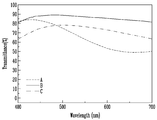
도 2는 다양한 실시 예에 따른 투명 전극들의 가시광 투과율을 나타내는 그래프.
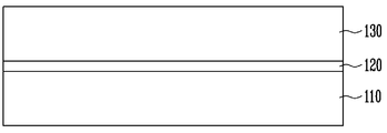
120: 2종류 이상의 금속을 포함하는 금속층
Claims (10)
- 제1 투명 산화물층;
상기 제1 투명 산화물층 상에 형성된 제2 투명 산화물층; 및
상기 제1 투명 산화물층 및 상기 제2 투명 산화물층 사이에 형성되며, 적어도 2종류의 금속을 포함하는 금속층을 포함하는 투명전극. - 제 1 항에 있어서,
상기 제1 투명 산화물층 및 상기 제2 투명 산화물층은 아연 산화물 또는 주석 산화물을 포함하는 투명전극. - 제 1 항에 있어서,
상기 금속층은 알루미늄과 은을 포함하는 투명전극. - 제 1 항에 있어서,
상기 금속층은 제1 알루미늄층, 상기 제1 알루미늄층 상에 형성된 은층 및 상기 은층 상에 형성된 제2 알루미늄층을 포함하는 3중층 구조로 형성된 투명전극. - 제 1 항에 있어서,
상기 금속층은 알루미늄과 은의 합성물을 포함하는 투명전극. - 제 5 항에 있어서,
상기 합성물은 상기 알루미늄을 12 내지 30 at.%의 비율로 포함하는 투명전극. - 제1 투명 산화물층을 형성하는 단계;
적어도 2종류의 금속을 스퍼터링하여 상기 제1 투명 산화물층 상에 금속층을 형성하는 단계; 및
상기 금속층 상에 제2 투명 산화물층을 형성하는 단계를 포함하는 투명전극 제조방법. - 제 7 항에 있어서,
상기 금속층을 형성하는 단계는
알루미늄과 은을 동시에 스퍼터링하여 상기 알루미늄과 상기 은의 합성물을 형성하는 단계를 포함하는 투명전극 제조방법. - 제 8 항에 있어서,
상기 합성물을 형성하는 단계는
1 내지 15%의 질소 또는 산소를 포함하는 아르곤 가스 분위기에서 스퍼터링 방식으로 실시되는 투명전극 제조방법. - 제 7 항에 있어서,
상기 금속층을 형성하는 단계는
상기 제1 알루미늄층을 형성하는 단계;
상기 제1 알루미늄층 상에 은층을 형성하는 단계; 및
상기 은층 상에 제2 알루미늄층을 형성하는 단계를 포함하는 투명전극 제조방법.
Priority Applications (1)
| Application Number | Priority Date | Filing Date | Title |
|---|---|---|---|
| KR1020140027786A KR20150105798A (ko) | 2014-03-10 | 2014-03-10 | 투명전극 및 그 제조방법 |
Applications Claiming Priority (1)
| Application Number | Priority Date | Filing Date | Title |
|---|---|---|---|
| KR1020140027786A KR20150105798A (ko) | 2014-03-10 | 2014-03-10 | 투명전극 및 그 제조방법 |
Publications (1)
| Publication Number | Publication Date |
|---|---|
| KR20150105798A true KR20150105798A (ko) | 2015-09-18 |
Family
ID=54244903
Family Applications (1)
| Application Number | Title | Priority Date | Filing Date |
|---|---|---|---|
| KR1020140027786A Ceased KR20150105798A (ko) | 2014-03-10 | 2014-03-10 | 투명전극 및 그 제조방법 |
Country Status (1)
| Country | Link |
|---|---|
| KR (1) | KR20150105798A (ko) |
Cited By (4)
| Publication number | Priority date | Publication date | Assignee | Title |
|---|---|---|---|---|
| US10338436B2 (en) | 2016-09-22 | 2019-07-02 | Samsung Display Co., Ltd. | Method of manufacturing curved liquid crystal display device and curved liquid crystal display device |
| US10423259B2 (en) | 2016-09-23 | 2019-09-24 | Samsung Display Co., Ltd. | Display apparatus including conductive layer having flexibility |
| KR20190124605A (ko) * | 2018-04-26 | 2019-11-05 | 세종대학교산학협력단 | 태양전지 제조방법 |
| KR20200098907A (ko) * | 2019-02-13 | 2020-08-21 | 인천대학교 산학협력단 | 투명 광전지 및 그 제조 방법 |
-
2014
- 2014-03-10 KR KR1020140027786A patent/KR20150105798A/ko not_active Ceased
Cited By (4)
| Publication number | Priority date | Publication date | Assignee | Title |
|---|---|---|---|---|
| US10338436B2 (en) | 2016-09-22 | 2019-07-02 | Samsung Display Co., Ltd. | Method of manufacturing curved liquid crystal display device and curved liquid crystal display device |
| US10423259B2 (en) | 2016-09-23 | 2019-09-24 | Samsung Display Co., Ltd. | Display apparatus including conductive layer having flexibility |
| KR20190124605A (ko) * | 2018-04-26 | 2019-11-05 | 세종대학교산학협력단 | 태양전지 제조방법 |
| KR20200098907A (ko) * | 2019-02-13 | 2020-08-21 | 인천대학교 산학협력단 | 투명 광전지 및 그 제조 방법 |
Similar Documents
| Publication | Publication Date | Title |
|---|---|---|
| CN102779944B (zh) | 一种透明导电薄膜 | |
| WO2017212970A1 (ja) | 積層膜、表示装置及び入力装置 | |
| WO2014115770A1 (ja) | 透明導電性基材ならびにその製造方法 | |
| KR101700884B1 (ko) | 망간주석산화물계 투명전도성산화물 및 이를 이용한 다층투명도전막 그리고 그 제조방법 | |
| KR20150039373A (ko) | 투명전극 및 이를 포함하는 전자 소자 | |
| KR20150105798A (ko) | 투명전극 및 그 제조방법 | |
| JP6511876B2 (ja) | 積層型透明導電膜 | |
| KR20110105048A (ko) | 투명 도전막, 그를 포함하는 디스플레이 필터 및 태양전지 | |
| EP4160624B1 (en) | Double-sided conductive film, coating method, and touch screen | |
| KR102032011B1 (ko) | 전도성 적층체 및 이를 포함하는 투명 전극 | |
| KR20140011854A (ko) | 마그네슘 산화아연을 포함하는 다층 투명 전극 및 이의 제조방법 | |
| KR20140090876A (ko) | 다층 구조의 투명 전극 | |
| CN105845752B (zh) | 一种应用于柔性光电器件的透明导电薄膜及其制备方法 | |
| KR20150075173A (ko) | 투명 전도성 산화물과 은 나노 와이어를 포함하는 투명 전극 및 그 제조방법 | |
| KR20200122447A (ko) | 질소 도핑된 산화물 기반 다층 투명전극 및 그 제조방법 | |
| JP2005047178A (ja) | 導電性を有する多層膜付透明基板 | |
| KR20180000173A (ko) | 투명전극 | |
| WO2016111125A1 (ja) | 熱電変換装置及び蓄電システム | |
| JP2007163995A (ja) | 透明導電膜付き基板およびその製造方法 | |
| KR20150135977A (ko) | 투명 전극 및 이를 포함하는 전자 소자 | |
| KR101816972B1 (ko) | TiO2/Ag/TiO2 다층박막 구조를 갖는 플렉시블 투명 전극 및 그 제조방법 | |
| CN214152473U (zh) | 一种双面导电膜及触控屏 | |
| TW201526025A (zh) | 複合導電薄膜 | |
| KR101832521B1 (ko) | 투명전극 및 이를 포함하는 전자 소자 | |
| WO2015159805A1 (ja) | 積層体、導電性積層体、および電子機器 |
Legal Events
| Date | Code | Title | Description |
|---|---|---|---|
| PA0109 | Patent application |
Patent event code: PA01091R01D Comment text: Patent Application Patent event date: 20140310 |
|
| PG1501 | Laying open of application | ||
| A201 | Request for examination | ||
| PA0201 | Request for examination |
Patent event code: PA02012R01D Patent event date: 20181224 Comment text: Request for Examination of Application Patent event code: PA02011R01I Patent event date: 20140310 Comment text: Patent Application |
|
| E902 | Notification of reason for refusal | ||
| PE0902 | Notice of grounds for rejection |
Comment text: Notification of reason for refusal Patent event date: 20200420 Patent event code: PE09021S01D |
|
| E601 | Decision to refuse application | ||
| PE0601 | Decision on rejection of patent |
Patent event date: 20200928 Comment text: Decision to Refuse Application Patent event code: PE06012S01D Patent event date: 20200420 Comment text: Notification of reason for refusal Patent event code: PE06011S01I |