KR20150109143A - 버퍼 구조물을 구비하는 발광 소자 및 이의 제조 방법 - Google Patents
버퍼 구조물을 구비하는 발광 소자 및 이의 제조 방법 Download PDFInfo
- Publication number
- KR20150109143A KR20150109143A KR1020140032223A KR20140032223A KR20150109143A KR 20150109143 A KR20150109143 A KR 20150109143A KR 1020140032223 A KR1020140032223 A KR 1020140032223A KR 20140032223 A KR20140032223 A KR 20140032223A KR 20150109143 A KR20150109143 A KR 20150109143A
- Authority
- KR
- South Korea
- Prior art keywords
- layer
- buffer structure
- light emitting
- emitting element
- conductive type
- Prior art date
- Legal status (The legal status is an assumption and is not a legal conclusion. Google has not performed a legal analysis and makes no representation as to the accuracy of the status listed.)
- Withdrawn
Links
Images


Classifications
-
- H—ELECTRICITY
- H10—SEMICONDUCTOR DEVICES; ELECTRIC SOLID-STATE DEVICES NOT OTHERWISE PROVIDED FOR
- H10H—INORGANIC LIGHT-EMITTING SEMICONDUCTOR DEVICES HAVING POTENTIAL BARRIERS
- H10H20/00—Individual inorganic light-emitting semiconductor devices having potential barriers, e.g. light-emitting diodes [LED]
- H10H20/80—Constructional details
- H10H20/81—Bodies
- H10H20/815—Bodies having stress relaxation structures, e.g. buffer layers
-
- H—ELECTRICITY
- H10—SEMICONDUCTOR DEVICES; ELECTRIC SOLID-STATE DEVICES NOT OTHERWISE PROVIDED FOR
- H10P—GENERIC PROCESSES OR APPARATUS FOR THE MANUFACTURE OR TREATMENT OF DEVICES COVERED BY CLASS H10
- H10P14/00—Formation of materials, e.g. in the shape of layers or pillars
- H10P14/20—Formation of materials, e.g. in the shape of layers or pillars of semiconductor materials
- H10P14/34—Deposited materials, e.g. layers
- H10P14/3402—Deposited materials, e.g. layers characterised by the chemical composition
- H10P14/3414—Deposited materials, e.g. layers characterised by the chemical composition being group IIIA-VIA materials
- H10P14/3416—Nitrides
-
- H—ELECTRICITY
- H10—SEMICONDUCTOR DEVICES; ELECTRIC SOLID-STATE DEVICES NOT OTHERWISE PROVIDED FOR
- H10H—INORGANIC LIGHT-EMITTING SEMICONDUCTOR DEVICES HAVING POTENTIAL BARRIERS
- H10H20/00—Individual inorganic light-emitting semiconductor devices having potential barriers, e.g. light-emitting diodes [LED]
- H10H20/01—Manufacture or treatment
- H10H20/011—Manufacture or treatment of bodies, e.g. forming semiconductor layers
- H10H20/013—Manufacture or treatment of bodies, e.g. forming semiconductor layers having light-emitting regions comprising only Group III-V materials
- H10H20/0133—Manufacture or treatment of bodies, e.g. forming semiconductor layers having light-emitting regions comprising only Group III-V materials with a substrate not being Group III-V materials
- H10H20/01335—Manufacture or treatment of bodies, e.g. forming semiconductor layers having light-emitting regions comprising only Group III-V materials with a substrate not being Group III-V materials the light-emitting regions comprising nitride materials
-
- H—ELECTRICITY
- H10—SEMICONDUCTOR DEVICES; ELECTRIC SOLID-STATE DEVICES NOT OTHERWISE PROVIDED FOR
- H10H—INORGANIC LIGHT-EMITTING SEMICONDUCTOR DEVICES HAVING POTENTIAL BARRIERS
- H10H20/00—Individual inorganic light-emitting semiconductor devices having potential barriers, e.g. light-emitting diodes [LED]
- H10H20/80—Constructional details
- H10H20/81—Bodies
- H10H20/814—Bodies having reflecting means, e.g. semiconductor Bragg reflectors
-
- H—ELECTRICITY
- H10—SEMICONDUCTOR DEVICES; ELECTRIC SOLID-STATE DEVICES NOT OTHERWISE PROVIDED FOR
- H10H—INORGANIC LIGHT-EMITTING SEMICONDUCTOR DEVICES HAVING POTENTIAL BARRIERS
- H10H20/00—Individual inorganic light-emitting semiconductor devices having potential barriers, e.g. light-emitting diodes [LED]
- H10H20/80—Constructional details
- H10H20/81—Bodies
- H10H20/819—Bodies characterised by their shape, e.g. curved or truncated substrates
- H10H20/82—Roughened surfaces, e.g. at the interface between epitaxial layers
-
- H—ELECTRICITY
- H10—SEMICONDUCTOR DEVICES; ELECTRIC SOLID-STATE DEVICES NOT OTHERWISE PROVIDED FOR
- H10H—INORGANIC LIGHT-EMITTING SEMICONDUCTOR DEVICES HAVING POTENTIAL BARRIERS
- H10H20/00—Individual inorganic light-emitting semiconductor devices having potential barriers, e.g. light-emitting diodes [LED]
- H10H20/80—Constructional details
- H10H20/81—Bodies
- H10H20/822—Materials of the light-emitting regions
- H10H20/824—Materials of the light-emitting regions comprising only Group III-V materials, e.g. GaP
- H10H20/825—Materials of the light-emitting regions comprising only Group III-V materials, e.g. GaP containing nitrogen, e.g. GaN
-
- H—ELECTRICITY
- H10—SEMICONDUCTOR DEVICES; ELECTRIC SOLID-STATE DEVICES NOT OTHERWISE PROVIDED FOR
- H10P—GENERIC PROCESSES OR APPARATUS FOR THE MANUFACTURE OR TREATMENT OF DEVICES COVERED BY CLASS H10
- H10P10/00—Bonding of wafers, substrates or parts of devices
- H10P10/14—Bonding of semiconductor wafers to insulating substrates
-
- H—ELECTRICITY
- H10—SEMICONDUCTOR DEVICES; ELECTRIC SOLID-STATE DEVICES NOT OTHERWISE PROVIDED FOR
- H10P—GENERIC PROCESSES OR APPARATUS FOR THE MANUFACTURE OR TREATMENT OF DEVICES COVERED BY CLASS H10
- H10P14/00—Formation of materials, e.g. in the shape of layers or pillars
- H10P14/20—Formation of materials, e.g. in the shape of layers or pillars of semiconductor materials
- H10P14/29—Formation of materials, e.g. in the shape of layers or pillars of semiconductor materials characterised by the substrates
- H10P14/2901—Materials
- H10P14/2902—Materials being Group IVA materials
- H10P14/2905—Silicon, silicon germanium or germanium
-
- H—ELECTRICITY
- H10—SEMICONDUCTOR DEVICES; ELECTRIC SOLID-STATE DEVICES NOT OTHERWISE PROVIDED FOR
- H10P—GENERIC PROCESSES OR APPARATUS FOR THE MANUFACTURE OR TREATMENT OF DEVICES COVERED BY CLASS H10
- H10P14/00—Formation of materials, e.g. in the shape of layers or pillars
- H10P14/20—Formation of materials, e.g. in the shape of layers or pillars of semiconductor materials
- H10P14/32—Formation of materials, e.g. in the shape of layers or pillars of semiconductor materials characterised by intermediate layers between substrates and deposited layers
- H10P14/3202—Materials thereof
- H10P14/3214—Materials thereof being Group IIIA-VA semiconductors
- H10P14/3216—Nitrides
-
- H—ELECTRICITY
- H10—SEMICONDUCTOR DEVICES; ELECTRIC SOLID-STATE DEVICES NOT OTHERWISE PROVIDED FOR
- H10P—GENERIC PROCESSES OR APPARATUS FOR THE MANUFACTURE OR TREATMENT OF DEVICES COVERED BY CLASS H10
- H10P14/00—Formation of materials, e.g. in the shape of layers or pillars
- H10P14/20—Formation of materials, e.g. in the shape of layers or pillars of semiconductor materials
- H10P14/32—Formation of materials, e.g. in the shape of layers or pillars of semiconductor materials characterised by intermediate layers between substrates and deposited layers
- H10P14/3202—Materials thereof
- H10P14/3238—Materials thereof being insulating materials
-
- H—ELECTRICITY
- H10—SEMICONDUCTOR DEVICES; ELECTRIC SOLID-STATE DEVICES NOT OTHERWISE PROVIDED FOR
- H10P—GENERIC PROCESSES OR APPARATUS FOR THE MANUFACTURE OR TREATMENT OF DEVICES COVERED BY CLASS H10
- H10P14/00—Formation of materials, e.g. in the shape of layers or pillars
- H10P14/20—Formation of materials, e.g. in the shape of layers or pillars of semiconductor materials
- H10P14/32—Formation of materials, e.g. in the shape of layers or pillars of semiconductor materials characterised by intermediate layers between substrates and deposited layers
- H10P14/3242—Structure
- H10P14/3244—Layer structure
- H10P14/3251—Layer structure consisting of three or more layers
- H10P14/3252—Alternating layers, e.g. superlattice
Landscapes
- Led Devices (AREA)
Abstract
Description
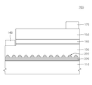
도 2는 본 발명의 다른 실시 예에 따르는 발광 소자를 개략적으로 나타내는 단면도이다.
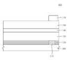
도 3은 본 발명의 또다른 실시 예에 따르는 발광 소자를 개략적으로 나타내는 단면도이다.
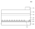
도 4는 본 발명의 또다른 실시 예에 따르는 발광 소자를 개략적으로 나타내는 단면도이다.
도 5는 본 발명의 일 실시 예에 따르는 버퍼 구조물의 반사율을 나타내는 그래프이다.
도 6은 본 발명의 일 실시 예에 따르는 발광 소자의 제조 방법을 개략적으로 나타내는 순서도이다.
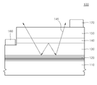
110: 기판, 120 220: 버퍼 구조물,
130: 제1 도전형 질화물 반도체층, 140: 활성층,
150: 제2 도전형 질화물 반도체층,
160 360: 제1 전극층,
170: 제2 전극층, 222: 요철 패턴.
Claims (21)
- 서로 번갈아 적층되는 산화실리콘층 및 질화알루미늄층을 포함하는 버퍼 구조물; 및
상기 버퍼 구조물 상에 순차적으로 배치되는 제1 도전형 질화물 반도체층, 활성층, 및 제2 도전형 질화물 반도체층을 포함하되,
상기 버퍼 구조물의 상층은 상기 질화알루미늄층인 발광 소자. - 제1 항에 있어서,
상기 버퍼 구조물은 상기 산화실리콘층과 상기 질화알루미늄층으로 이루어지는 단위적층구조체가 복수의 쌍(pair)으로 적층되는
발광 소자. - 제2 항에 있어서,
상기 버퍼 구조물은 80 내지 90 nm의 두께를 가지는 단위적층구조체가 10 내지 100 쌍으로 적층되는
발광 소자. - 제1 항에 있어서,
상기 버퍼 구조물은 상기 버퍼 구조물로 입사하는 광을 반사시키는 분산형 브래그 반사층(DBR)으로 기능하는
발광 소자. - 제4 항에 있어서,
상기 버퍼 구조물은 400 nm 내지 800 nm의 파장 범위를 가지는 광에 대해 적어도 90% 이상의 반사율을 가지는
발광 소자. - 제1 항에 있어서,
상기 버퍼 구조물의 하부에 배치되어, 상기 버퍼 구조물이 적층되도록 하는 기판을 더 포함하는
발광 소자. - 제1 항에 있어서,
상기 버퍼구조물은 상기 제1 도전형 질화물 반도체와의 계면에 요철 패턴을 구비하는
발광 소자. - 제7 항에 있어서,
상기 요철 패턴의 요부 및 철부는 상기 버퍼 구조물의 상기 질화알루미늄층을 노출시키는
발광 소자. - 기판;
상기 기판 상에서 서로 번갈아 적층되는 산화실리콘층 및 질화알루미늄층을 포함하고, 분산형 브래그 반사층을 구비하는 버퍼 구조물; 및
상기 버퍼 구조물 상에 순차적으로 배치되는 제1 도전형 질화갈륨층, 활성층, 및 제2 도전형 질화갈륨층을 포함하되,
상기 버퍼 구조물은 상기 기판과 상기 제1 도전형 질화갈륨층 사이에서 완층층으로 기능하는
발광 소자. - 제9 항에 있어서,
상기 기판은
사파이어 기판, 탄화실리콘(SiC) 기판 및 실리콘 기판 중 어느 하나인
발광 소자. - 제9 항에 있어서,
상기 버퍼 구조물은 상기 산화실리콘층과 상기 질화알루미늄층으로 이루어지는 단위적층구조체의 복층 구조물을 포함하는
발광 소자. - 제11 항에 있어서,
상기 버퍼 구조물은 80 내지 90 nm의 두께를 가지는 단위적층구조체가 10 내지 100의 쌍으로 적층되는
발광 소자. - 제9 항에 있어서,
상기 버퍼 구조물은 400 nm 내지 800 nm의 파장 범위를 가지는 광에 대해 적어도 90% 이상의 반사율을 가지는
발광 소자.
? - 제9 항에 있어서,
상기 버퍼구조물은 상기 제1 도전형 갈륨질화층과의 계면에 요철 패턴을 구비하는
발광 소자. - 제14 항에 있어서,
상기 요철 패턴의 요부 및 철부는 상기 버퍼 구조물의 상기 질화알루미늄층을 노출시키는
발광 소자. - 제9 항에 있어서,
상기 산화실리콘층은 비정질 구조를 가지며,
상기 질화알루미늄층은 결정질 구조를 가지는
발광 소자. - 제9 항에 있어서,
상기 버퍼 구조물의 상기 질화알루미늄층은 상기 제1 도전형 질화갈륨층의 에피텍셜 성장을 돕는
발광 소자. - 기판을 준비하는 단계;
상기 기판 상에서 서로 번갈아 적층되는 산화실리콘층 및 질화알루미늄층을 포함하는 버퍼 구조물을 형성하는 단계;
상기 버퍼 구조물 상에 순차적으로 제1 도전형 질화물 반도체층, 활성층 및 제2 도전형 질화물 반도체층을 적층하는 단계를 포함하되,
상기 버퍼 구조물의 상기 질화알루미늄층과 상기 제1 도전형 질화물 반도체층을 서로 접하도록 형성하는
발광 소자의 제조 방법. - 제18 항에 있어서,
상기 버퍼 구조물은 80 내지 90 nm의 두께를 가지는 산화실리콘층 및 질화알루미늄층의 단위적층구조체가 10 내지 100의 쌍으로 적층되는
발광 소자의 제조 방법. - 제18 항에 있어서,
상기 버퍼 구조물을 형성한 후에,
상기 실리콘산화층 및 상기 알루미늄질화층을 선택적으로 식각하여, 요철 구조를 형성하는 단계를 더 포함하는
발광 소자의 제조 방법. - 제20 항에 있어서,
상기 제2 도전형 질화물 반도체층을 형성한 후에,
상기 기판을 제거하는 단계를 더 포함하는
발광 소자의 제조 방법.
Priority Applications (1)
| Application Number | Priority Date | Filing Date | Title |
|---|---|---|---|
| KR1020140032223A KR20150109143A (ko) | 2014-03-19 | 2014-03-19 | 버퍼 구조물을 구비하는 발광 소자 및 이의 제조 방법 |
Applications Claiming Priority (1)
| Application Number | Priority Date | Filing Date | Title |
|---|---|---|---|
| KR1020140032223A KR20150109143A (ko) | 2014-03-19 | 2014-03-19 | 버퍼 구조물을 구비하는 발광 소자 및 이의 제조 방법 |
Publications (1)
| Publication Number | Publication Date |
|---|---|
| KR20150109143A true KR20150109143A (ko) | 2015-10-01 |
Family
ID=54338254
Family Applications (1)
| Application Number | Title | Priority Date | Filing Date |
|---|---|---|---|
| KR1020140032223A Withdrawn KR20150109143A (ko) | 2014-03-19 | 2014-03-19 | 버퍼 구조물을 구비하는 발광 소자 및 이의 제조 방법 |
Country Status (1)
| Country | Link |
|---|---|
| KR (1) | KR20150109143A (ko) |
Cited By (1)
| Publication number | Priority date | Publication date | Assignee | Title |
|---|---|---|---|---|
| KR20240098883A (ko) * | 2022-12-21 | 2024-06-28 | 엘지전자 주식회사 | 화소용 반도체 발광 소자 및 이를 포함하는 디스플레이 장치 |
-
2014
- 2014-03-19 KR KR1020140032223A patent/KR20150109143A/ko not_active Withdrawn
Cited By (1)
| Publication number | Priority date | Publication date | Assignee | Title |
|---|---|---|---|---|
| KR20240098883A (ko) * | 2022-12-21 | 2024-06-28 | 엘지전자 주식회사 | 화소용 반도체 발광 소자 및 이를 포함하는 디스플레이 장치 |
Similar Documents
| Publication | Publication Date | Title |
|---|---|---|
| US11929451B2 (en) | Semiconductor light emitting device | |
| US20230163159A1 (en) | Monolithic led array and a precursor thereto | |
| US10062821B2 (en) | Light-emitting device | |
| KR101898679B1 (ko) | 나노구조 발광소자 | |
| KR101258583B1 (ko) | 나노 로드 발광 소자 및 그 제조 방법 | |
| US8405103B2 (en) | Photonic crystal light emitting device and manufacturing method of the same | |
| JP5237286B2 (ja) | フォトニック結晶により定められたアレイ状エミッタを含む発光デバイス | |
| US7674639B2 (en) | GaN based LED with etched exposed surface for improved light extraction efficiency and method for making the same | |
| TWI431802B (zh) | 光電半導體本件 | |
| TWI452731B (zh) | 光電半導體晶片及其製造方法 | |
| JP5623074B2 (ja) | 光電子半導体部品 | |
| CN106463574B (zh) | 具有图案化衬底的发光器件 | |
| KR20220140749A (ko) | 적색 led 및 제작 방법 | |
| US11437427B2 (en) | Light-emitting device and manufacturing method thereof | |
| CN103325904B (zh) | 包括氮化物基半导体全方向反射器的发光装置 | |
| US10862004B2 (en) | Ultraviolet semiconductor light emitting devices | |
| JP7418583B2 (ja) | モノリシック発光ダイオード前駆体を形成する方法 | |
| JP2011228628A (ja) | 垂直型の光抽出メカニズムを備える発光素子及びその製造方法 | |
| KR20230058638A (ko) | Led 디바이스 및 led 디바이스를 제조하는 방법 | |
| JPWO2011058890A1 (ja) | 発光素子 | |
| US8664020B2 (en) | Semiconductor light emitting device and method of manufacturing the same | |
| US20120080707A1 (en) | Semiconductor light emitting device and manufacturing method thereof | |
| US9306120B2 (en) | High efficiency light emitting diode | |
| TW202205467A (zh) | 單體電子器件 | |
| KR20150109143A (ko) | 버퍼 구조물을 구비하는 발광 소자 및 이의 제조 방법 |
Legal Events
| Date | Code | Title | Description |
|---|---|---|---|
| PA0109 | Patent application |
St.27 status event code: A-0-1-A10-A12-nap-PA0109 |
|
| R18-X000 | Changes to party contact information recorded |
St.27 status event code: A-3-3-R10-R18-oth-X000 |
|
| PN2301 | Change of applicant |
St.27 status event code: A-3-3-R10-R13-asn-PN2301 St.27 status event code: A-3-3-R10-R11-asn-PN2301 |
|
| PG1501 | Laying open of application |
St.27 status event code: A-1-1-Q10-Q12-nap-PG1501 |
|
| R17-X000 | Change to representative recorded |
St.27 status event code: A-3-3-R10-R17-oth-X000 |
|
| P22-X000 | Classification modified |
St.27 status event code: A-2-2-P10-P22-nap-X000 |
|
| PC1203 | Withdrawal of no request for examination |
St.27 status event code: N-1-6-B10-B12-nap-PC1203 |
|
| WITN | Application deemed withdrawn, e.g. because no request for examination was filed or no examination fee was paid | ||
| P22-X000 | Classification modified |
St.27 status event code: A-2-2-P10-P22-nap-X000 |
|
| P22-X000 | Classification modified |
St.27 status event code: A-2-2-P10-P22-nap-X000 |