KR20150120334A - 고체 촬상 장치 및 고체 촬상 장치의 제조 방법 - Google Patents
고체 촬상 장치 및 고체 촬상 장치의 제조 방법 Download PDFInfo
- Publication number
- KR20150120334A KR20150120334A KR1020157017814A KR20157017814A KR20150120334A KR 20150120334 A KR20150120334 A KR 20150120334A KR 1020157017814 A KR1020157017814 A KR 1020157017814A KR 20157017814 A KR20157017814 A KR 20157017814A KR 20150120334 A KR20150120334 A KR 20150120334A
- Authority
- KR
- South Korea
- Prior art keywords
- solid
- pattern
- axis direction
- imaging device
- patterns
- Prior art date
- Legal status (The legal status is an assumption and is not a legal conclusion. Google has not performed a legal analysis and makes no representation as to the accuracy of the status listed.)
- Granted
Links
Images


Classifications
-
- H01L27/14607—
-
- G—PHYSICS
- G03—PHOTOGRAPHY; CINEMATOGRAPHY; ANALOGOUS TECHNIQUES USING WAVES OTHER THAN OPTICAL WAVES; ELECTROGRAPHY; HOLOGRAPHY
- G03F—PHOTOMECHANICAL PRODUCTION OF TEXTURED OR PATTERNED SURFACES, e.g. FOR PRINTING, FOR PROCESSING OF SEMICONDUCTOR DEVICES; MATERIALS THEREFOR; ORIGINALS THEREFOR; APPARATUS SPECIALLY ADAPTED THEREFOR
- G03F7/00—Photomechanical, e.g. photolithographic, production of textured or patterned surfaces, e.g. printing surfaces; Materials therefor, e.g. comprising photoresists; Apparatus specially adapted therefor
- G03F7/20—Exposure; Apparatus therefor
-
- H01L27/14605—
-
- H01L27/14812—
-
- H—ELECTRICITY
- H04—ELECTRIC COMMUNICATION TECHNIQUE
- H04N—PICTORIAL COMMUNICATION, e.g. TELEVISION
- H04N25/00—Circuitry of solid-state image sensors [SSIS]; Control thereof
- H04N25/70—SSIS architectures; Circuits associated therewith
-
- H—ELECTRICITY
- H10—SEMICONDUCTOR DEVICES; ELECTRIC SOLID-STATE DEVICES NOT OTHERWISE PROVIDED FOR
- H10F—INORGANIC SEMICONDUCTOR DEVICES SENSITIVE TO INFRARED RADIATION, LIGHT, ELECTROMAGNETIC RADIATION OF SHORTER WAVELENGTH OR CORPUSCULAR RADIATION
- H10F39/00—Integrated devices, or assemblies of multiple devices, comprising at least one element covered by group H10F30/00, e.g. radiation detectors comprising photodiode arrays
- H10F39/011—Manufacture or treatment of image sensors covered by group H10F39/12
-
- H—ELECTRICITY
- H10—SEMICONDUCTOR DEVICES; ELECTRIC SOLID-STATE DEVICES NOT OTHERWISE PROVIDED FOR
- H10F—INORGANIC SEMICONDUCTOR DEVICES SENSITIVE TO INFRARED RADIATION, LIGHT, ELECTROMAGNETIC RADIATION OF SHORTER WAVELENGTH OR CORPUSCULAR RADIATION
- H10F39/00—Integrated devices, or assemblies of multiple devices, comprising at least one element covered by group H10F30/00, e.g. radiation detectors comprising photodiode arrays
- H10F39/10—Integrated devices
- H10F39/12—Image sensors
- H10F39/15—Charge-coupled device [CCD] image sensors
- H10F39/151—Geometry or disposition of pixel elements, address lines or gate electrodes
-
- H—ELECTRICITY
- H10—SEMICONDUCTOR DEVICES; ELECTRIC SOLID-STATE DEVICES NOT OTHERWISE PROVIDED FOR
- H10F—INORGANIC SEMICONDUCTOR DEVICES SENSITIVE TO INFRARED RADIATION, LIGHT, ELECTROMAGNETIC RADIATION OF SHORTER WAVELENGTH OR CORPUSCULAR RADIATION
- H10F39/00—Integrated devices, or assemblies of multiple devices, comprising at least one element covered by group H10F30/00, e.g. radiation detectors comprising photodiode arrays
- H10F39/10—Integrated devices
- H10F39/12—Image sensors
- H10F39/15—Charge-coupled device [CCD] image sensors
- H10F39/153—Two-dimensional or three-dimensional array CCD image sensors
-
- H—ELECTRICITY
- H10—SEMICONDUCTOR DEVICES; ELECTRIC SOLID-STATE DEVICES NOT OTHERWISE PROVIDED FOR
- H10F—INORGANIC SEMICONDUCTOR DEVICES SENSITIVE TO INFRARED RADIATION, LIGHT, ELECTROMAGNETIC RADIATION OF SHORTER WAVELENGTH OR CORPUSCULAR RADIATION
- H10F39/00—Integrated devices, or assemblies of multiple devices, comprising at least one element covered by group H10F30/00, e.g. radiation detectors comprising photodiode arrays
- H10F39/10—Integrated devices
- H10F39/12—Image sensors
- H10F39/15—Charge-coupled device [CCD] image sensors
- H10F39/153—Two-dimensional or three-dimensional array CCD image sensors
- H10F39/1538—Time-delay and integration
-
- H—ELECTRICITY
- H10—SEMICONDUCTOR DEVICES; ELECTRIC SOLID-STATE DEVICES NOT OTHERWISE PROVIDED FOR
- H10F—INORGANIC SEMICONDUCTOR DEVICES SENSITIVE TO INFRARED RADIATION, LIGHT, ELECTROMAGNETIC RADIATION OF SHORTER WAVELENGTH OR CORPUSCULAR RADIATION
- H10F39/00—Integrated devices, or assemblies of multiple devices, comprising at least one element covered by group H10F30/00, e.g. radiation detectors comprising photodiode arrays
- H10F39/80—Constructional details of image sensors
Landscapes
- Engineering & Computer Science (AREA)
- Multimedia (AREA)
- Signal Processing (AREA)
- Solid State Image Pick-Up Elements (AREA)
- Exposure And Positioning Against Photoresist Photosensitive Materials (AREA)
- Physics & Mathematics (AREA)
- General Physics & Mathematics (AREA)
Abstract
Description
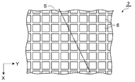
도 2는 도 1의 일부분을 확대하여 나타내는 도면이다.
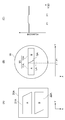
도 3은 일 실시 형태에 따른 고체 촬상 장치의 제조 방법에 있어서 사용되는 포토마스크(photomask)의 패턴의 형상을 나타내는 개략도이다.
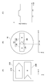
도 4는 포토마스크의 패턴의 다른 형상을 나타내는 개략도이다.
도 5는 포토마스크의 패턴의 다른 형상을 나타내는 개략도이다.
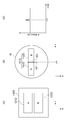
도 6은 비교예에 따른 포토마스크의 패턴의 형상을 나타내는 개략도이다.
도 7은 다른 비교예에 따른 포토마스크의 패턴의 형상을 나타내는 개략도이다.
2A, 2B, 11A, 12A, 11B, 12B, 11C~15C … 패턴,
3 … 수평 전송부, 6 … 화소,
W … 웨이퍼(반도체 기판).
Claims (4)
- 반도체 기판상에 복수의 패턴이 제1 방향으로 서로 이어지도록 노광되어 형성된 수광부를 구비한 고체 촬상 장치로서,
상기 수광부는, 상기 제1 방향과 상기 제1 방향에 직교하는 제2 방향으로 2차원 모양으로 배열된 복수의 화소를 가지고, 상기 복수의 화소 중, 상기 제2 방향으로 배열된 복수의 화소로 이루어지는 화소 열마다, 전하를 제2 방향으로 전송하고 있고,
상기 수광부에서는, 상기 복수의 패턴이 서로 이어지는 경계가, 상기 제1 방향과 상기 제2 방향에 교차하는 방향으로 연장되는 1개 이상의 선분 위를 따라서 위치하고 있는 고체 촬상 장치. - 청구항 1에 있어서,
상기 복수의 패턴이 서로 이어지는 상기 경계는, 상기 제2 방향으로 연장되는 1개의 직선에 대해서, 한 지점에서만 교차하는 고체 촬상 장치. - 청구항 1 또는 청구항 2에 있어서,
TDI 구동이 가능한 고체 촬상 장치. - 반도체 기판상에 복수의 패턴을 제1 방향으로 서로 이어지도록 노광하여 수광부를 형성하는 스텝을 구비한 고체 촬상 장치의 제조 방법으로서,
상기 수광부는, 상기 제1 방향과 상기 제1 방향에 직교하는 제2 방향으로 2차원 모양으로 배열된 복수의 화소를 가지고, 상기 복수의 화소 중, 상기 제2 방향으로 배열된 복수의 화소로 이루어지는 화소 열마다, 전하를 제2 방향으로 전송하고 있고,
상기 수광부에서는, 상기 복수의 패턴이 서로 이어지는 경계가, 상기 제1 방향과 상기 제2 방향에 교차하는 방향으로 연장되는 1개 이상의 선분 위를 따라서 위치하고 있는 고체 촬상 장치의 제조 방법.
Applications Claiming Priority (3)
| Application Number | Priority Date | Filing Date | Title |
|---|---|---|---|
| JP2013025620A JP6110154B2 (ja) | 2013-02-13 | 2013-02-13 | 固体撮像装置及び固体撮像装置の製造方法 |
| JPJP-P-2013-025620 | 2013-02-13 | ||
| PCT/JP2014/053185 WO2014126100A1 (ja) | 2013-02-13 | 2014-02-12 | 固体撮像装置及び固体撮像装置の製造方法 |
Publications (2)
| Publication Number | Publication Date |
|---|---|
| KR20150120334A true KR20150120334A (ko) | 2015-10-27 |
| KR102128639B1 KR102128639B1 (ko) | 2020-06-30 |
Family
ID=51354099
Family Applications (1)
| Application Number | Title | Priority Date | Filing Date |
|---|---|---|---|
| KR1020157017814A Active KR102128639B1 (ko) | 2013-02-13 | 2014-02-12 | 고체 촬상 장치 및 고체 촬상 장치의 제조 방법 |
Country Status (7)
| Country | Link |
|---|---|
| US (1) | US9749561B2 (ko) |
| EP (1) | EP2958147B1 (ko) |
| JP (1) | JP6110154B2 (ko) |
| KR (1) | KR102128639B1 (ko) |
| CN (1) | CN104995735B (ko) |
| TW (1) | TWI652809B (ko) |
| WO (1) | WO2014126100A1 (ko) |
Families Citing this family (1)
| Publication number | Priority date | Publication date | Assignee | Title |
|---|---|---|---|---|
| TW202031539A (zh) * | 2019-02-25 | 2020-09-01 | 先進光電科技股份有限公司 | 行動載具輔助系統 |
Citations (5)
| Publication number | Priority date | Publication date | Assignee | Title |
|---|---|---|---|---|
| JP2000101061A (ja) | 1998-09-21 | 2000-04-07 | Hamamatsu Photonics Kk | 固体撮像装置 |
| JP2001077343A (ja) * | 1999-09-01 | 2001-03-23 | Sony Corp | Ccd撮像素子の製造装置及び製造方法 |
| JP2003347539A (ja) | 2002-05-27 | 2003-12-05 | Hamamatsu Photonics Kk | 固体撮像装置及び固体撮像装置アレイ |
| JP2010093331A (ja) * | 2008-10-03 | 2010-04-22 | Mitsubishi Electric Corp | イメージセンサ及びその駆動方法 |
| US20130057739A1 (en) * | 2011-02-24 | 2013-03-07 | Teledyne Dalsa, Inc. | Continuous clocking mode for tdi binning operation of ccd image sensor |
Family Cites Families (12)
| Publication number | Priority date | Publication date | Assignee | Title |
|---|---|---|---|---|
| US5298761A (en) | 1991-06-17 | 1994-03-29 | Nikon Corporation | Method and apparatus for exposure process |
| US6048785A (en) * | 1997-06-16 | 2000-04-11 | Advanced Micro Devices, Inc. | Semiconductor fabrication method of combining a plurality of fields defined by a reticle image using segment stitching |
| JP2003179221A (ja) * | 2001-12-11 | 2003-06-27 | Mitsubishi Electric Corp | リニアイメージセンサの製造方法及びその構造 |
| JP2003280173A (ja) * | 2002-03-26 | 2003-10-02 | Canon Inc | リソグラフィ用マスク及びそれを用いた半導体装置の製造方法及び半導体装置 |
| US20090268983A1 (en) * | 2005-07-25 | 2009-10-29 | The Regents Of The University Of California | Digital imaging system and method using multiple digital image sensors to produce large high-resolution gapless mosaic images |
| JP5214904B2 (ja) * | 2007-04-12 | 2013-06-19 | ルネサスエレクトロニクス株式会社 | 固体撮像素子の製造方法 |
| JP4462299B2 (ja) * | 2007-07-17 | 2010-05-12 | ソニー株式会社 | 撮像装置、および画像処理方法、並びにコンピュータ・プログラム |
| US7737390B2 (en) * | 2008-01-14 | 2010-06-15 | Tower Semiconductor, Ltd. | Horizontal row drivers for CMOS image sensor with tiling on three edges |
| JP5418810B2 (ja) * | 2008-02-14 | 2014-02-19 | ソニー株式会社 | クランプ制御方法、クランプ補正装置、イメージセンサ、および、電子機器 |
| US20120113213A1 (en) * | 2010-11-05 | 2012-05-10 | Teledyne Dalsa, Inc. | Wide format sensor |
| US8866890B2 (en) * | 2010-11-05 | 2014-10-21 | Teledyne Dalsa, Inc. | Multi-camera |
| JP5917883B2 (ja) * | 2011-11-02 | 2016-05-18 | 浜松ホトニクス株式会社 | 固体撮像装置 |
-
2013
- 2013-02-13 JP JP2013025620A patent/JP6110154B2/ja active Active
-
2014
- 2014-02-12 WO PCT/JP2014/053185 patent/WO2014126100A1/ja not_active Ceased
- 2014-02-12 EP EP14751421.0A patent/EP2958147B1/en active Active
- 2014-02-12 US US14/766,788 patent/US9749561B2/en active Active
- 2014-02-12 KR KR1020157017814A patent/KR102128639B1/ko active Active
- 2014-02-12 CN CN201480008752.0A patent/CN104995735B/zh active Active
- 2014-02-13 TW TW103104780A patent/TWI652809B/zh active
Patent Citations (5)
| Publication number | Priority date | Publication date | Assignee | Title |
|---|---|---|---|---|
| JP2000101061A (ja) | 1998-09-21 | 2000-04-07 | Hamamatsu Photonics Kk | 固体撮像装置 |
| JP2001077343A (ja) * | 1999-09-01 | 2001-03-23 | Sony Corp | Ccd撮像素子の製造装置及び製造方法 |
| JP2003347539A (ja) | 2002-05-27 | 2003-12-05 | Hamamatsu Photonics Kk | 固体撮像装置及び固体撮像装置アレイ |
| JP2010093331A (ja) * | 2008-10-03 | 2010-04-22 | Mitsubishi Electric Corp | イメージセンサ及びその駆動方法 |
| US20130057739A1 (en) * | 2011-02-24 | 2013-03-07 | Teledyne Dalsa, Inc. | Continuous clocking mode for tdi binning operation of ccd image sensor |
Also Published As
| Publication number | Publication date |
|---|---|
| US9749561B2 (en) | 2017-08-29 |
| EP2958147A1 (en) | 2015-12-23 |
| TWI652809B (zh) | 2019-03-01 |
| EP2958147B1 (en) | 2019-06-12 |
| JP2014154821A (ja) | 2014-08-25 |
| CN104995735A (zh) | 2015-10-21 |
| US20150365613A1 (en) | 2015-12-17 |
| KR102128639B1 (ko) | 2020-06-30 |
| JP6110154B2 (ja) | 2017-04-05 |
| EP2958147A4 (en) | 2016-09-28 |
| CN104995735B (zh) | 2018-06-19 |
| WO2014126100A1 (ja) | 2014-08-21 |
| TW201444072A (zh) | 2014-11-16 |
Similar Documents
| Publication | Publication Date | Title |
|---|---|---|
| US10636822B2 (en) | Photoelectric conversion element and solid-state image capturing device | |
| US9653498B2 (en) | Imaging device having electrode overlying photoelectric conversion layer and having electrical contact to electrode | |
| CN103137640B (zh) | 固态成像设备、照相机和固态成像设备的设计方法 | |
| US10068940B2 (en) | Imaging apparatus with focus-ranging precision in one direction due to saturated photoelectric conversion elements located adjacent to each other | |
| KR20160082682A (ko) | 전하 결합 소자 및 그 제조 방법 및 고체 촬상 장치 | |
| CN1848925A (zh) | 固体摄像装置 | |
| KR101445332B1 (ko) | 표시장치 | |
| JP5870104B2 (ja) | 複数の接点パターンを有するccdセンサ | |
| TWI537805B (zh) | 單層電容式觸控面板 | |
| KR20150120334A (ko) | 고체 촬상 장치 및 고체 촬상 장치의 제조 방법 | |
| CN111684600A (zh) | 用于照相机的像素阵列、照相机以及具有这种照相机的光传播时间照相机系统 | |
| CN109218577B (zh) | 光检测装置及摄像装置 | |
| WO2018116523A1 (ja) | Tdi方式リニアイメージセンサ | |
| CN107507843B (zh) | 一种像素结构及x射影像传感器 | |
| EP2963686A1 (en) | Semiconductor photodetection device | |
| US9635293B2 (en) | Solid-state imaging device | |
| US20210305312A1 (en) | Solid state imaging device | |
| JP5052421B2 (ja) | Tdi方式イメージセンサ、及びその駆動方法 | |
| JP5836376B2 (ja) | 複数の接点パターンを有するccdセンサ | |
| CN109216380B (zh) | 光检测装置及摄像装置 | |
| JP5943808B2 (ja) | Tdi方式リニアイメージセンサを用いた撮像システム、及びその駆動方法 | |
| JP2016025187A (ja) | 固体撮像装置及びその駆動方法、並びに電子機器 | |
| KR20080028155A (ko) | 이미지 센서 및 그 제조방법 | |
| JPS60157251A (ja) | 赤外線検知素子 | |
| JP2015041721A (ja) | 半導体装置 |
Legal Events
| Date | Code | Title | Description |
|---|---|---|---|
| PA0105 | International application |
Patent event date: 20150702 Patent event code: PA01051R01D Comment text: International Patent Application |
|
| PG1501 | Laying open of application | ||
| A201 | Request for examination | ||
| PA0201 | Request for examination |
Patent event code: PA02012R01D Patent event date: 20180912 Comment text: Request for Examination of Application |
|
| E902 | Notification of reason for refusal | ||
| PE0902 | Notice of grounds for rejection |
Comment text: Notification of reason for refusal Patent event date: 20191223 Patent event code: PE09021S01D |
|
| E701 | Decision to grant or registration of patent right | ||
| PE0701 | Decision of registration |
Patent event code: PE07011S01D Comment text: Decision to Grant Registration Patent event date: 20200511 |
|
| GRNT | Written decision to grant | ||
| PR0701 | Registration of establishment |
Comment text: Registration of Establishment Patent event date: 20200624 Patent event code: PR07011E01D |
|
| PR1002 | Payment of registration fee |
Payment date: 20200624 End annual number: 3 Start annual number: 1 |
|
| PG1601 | Publication of registration | ||
| PR1001 | Payment of annual fee |
Payment date: 20240520 Start annual number: 5 End annual number: 5 |